EP1136833A1 - Method of performing a burn-in process to electrically stress a semiconductor memory - Google Patents
Method of performing a burn-in process to electrically stress a semiconductor memory Download PDFInfo
- Publication number
- EP1136833A1 EP1136833A1 EP01104285A EP01104285A EP1136833A1 EP 1136833 A1 EP1136833 A1 EP 1136833A1 EP 01104285 A EP01104285 A EP 01104285A EP 01104285 A EP01104285 A EP 01104285A EP 1136833 A1 EP1136833 A1 EP 1136833A1
- Authority
- EP
- European Patent Office
- Prior art keywords
- voltage
- reference potential
- control
- burn
- circuit arrangement
- Prior art date
- Legal status (The legal status is an assumption and is not a legal conclusion. Google has not performed a legal analysis and makes no representation as to the accuracy of the status listed.)
- Granted
Links
- 238000000034 method Methods 0.000 title claims abstract description 36
- 239000004065 semiconductor Substances 0.000 title claims description 9
- 230000015654 memory Effects 0.000 claims description 16
- 230000035882 stress Effects 0.000 description 13
- 230000010363 phase shift Effects 0.000 description 5
- 230000032683 aging Effects 0.000 description 4
- 230000006399 behavior Effects 0.000 description 4
- 230000018109 developmental process Effects 0.000 description 3
- 238000010586 diagram Methods 0.000 description 3
- 239000002800 charge carrier Substances 0.000 description 2
- 230000006641 stabilisation Effects 0.000 description 2
- 238000011105 stabilization Methods 0.000 description 2
- 239000003990 capacitor Substances 0.000 description 1
- 230000000295 complement effect Effects 0.000 description 1
- 230000007423 decrease Effects 0.000 description 1
- 230000002950 deficient Effects 0.000 description 1
- 230000000694 effects Effects 0.000 description 1
- 230000006870 function Effects 0.000 description 1
- 238000002347 injection Methods 0.000 description 1
- 239000007924 injection Substances 0.000 description 1
- 230000005527 interface trap Effects 0.000 description 1
- 238000004519 manufacturing process Methods 0.000 description 1
- 239000002184 metal Substances 0.000 description 1
- 230000000737 periodic effect Effects 0.000 description 1
Images

Classifications
-
- G—PHYSICS
- G11—INFORMATION STORAGE
- G11C—STATIC STORES
- G11C29/00—Checking stores for correct operation ; Subsequent repair; Testing stores during standby or offline operation
- G11C29/04—Detection or location of defective memory elements, e.g. cell constructio details, timing of test signals
- G11C29/50—Marginal testing, e.g. race, voltage or current testing
Definitions
- the invention relates to a method for carrying out a Burn-in process for the electrical stressing of a semiconductor memory.
- a semiconductor memory is e.g. a DRAM (Dynamic Random Access memory). It comprises a cell array with memory cells and a control periphery.
- the memory cells of the memory cell array consist of a selection transistor and a storage capacitor.
- the control periphery is usually formed from transistors using CMOS technology are made.
- CMOS means Complementary Metal Oxyd Semiconductor and contains both N-MOS and P-MOS transistors be used.
- the mechanism on which the burn-in process according to the invention is dynamic stressing of a MOS transistor.
- Stressing a MOS transistor is e.g. its source connector to a reference potential, its drain connection to a Operating voltage and its gate connection to an alternating Voltage applied, the values between the reference potential and of the operating voltage.
- the voltage at the drain connection e.g. chosen greater than the voltage at the gate connection.
- the properties of a transistor change among them Stress conditions in a few hours as much as normal ones Operation in two years. This stabilizes his Input voltage and remains during its expected ten-year period Operating time at the customer during normal operation in the Memory constant.
- a through the Stress modified transistor in the memory circuit periphery be identified during the test phase, so that the defective memory is not delivered as a product. Under stress, for example, the threshold voltage of the transistor changes and stabilizes.
- combinatorial blocks are arranged in the circuit periphery, which contain transistors.
- control voltage voltage values between the reference potential and an operating voltage alternate.
- the circuit arrangement contains an inverter, the control voltage being applied to an inverter input a first inverter voltage supply the reference potential and the second to a second inverter voltage supply Voltage is applied.
- This arrangement achieves that a stressful transistor in the circuit arrangement is arranged.
- the circuit arrangement contains an inverter. It is an inverter Basic element of every CMOS circuit and is also in the Circuit periphery of a memory included. Farther are logic functions such as AND in the circuit blocks, NAND, OR, NOR, XOR etc. included.
- the second voltage indicates the value of the operating voltage.
- An advantageous embodiment of the method according to the invention provides that the applied to the second voltage connection second voltage between the reference potential and the operating voltage alternates. By alternating the second Voltage, the stress for the circuit arrangement is increased, so that the time to stress can be reduced and the same stress effect is achieved in less time.
- a further development of the method according to the invention provides before that the second voltage at a first frequency and the control voltage with a second frequency between the Alternate reference potential and operating voltage.
- the periodic Alternating the second voltage and the control voltage each with a fixed frequency enables simple circuit implementation of an arrangement to carry out a burn-in process.
- An advantageous embodiment of the method according to the invention stipulates that the first frequency be equal to the second frequency is, and the two voltages have a phase difference between Have 150 to 210 degrees.
- a phase difference of 180 degrees means that the two signals behave exactly in phase opposition.
- the tolerance range between 150 to 210 degrees phase shift enables a variation of the phase shift in the specified range, what a variety of stress constellations means for the circuit arrangement.
- phase difference is varied.
- phase difference there can be a variety of constellations of the operating voltage and control voltage be generated. This will stress the circuitry further increases what the time for the burn-in process reduced.
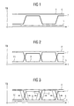
- FIG 4 is a circuit arrangement 1 with a first Voltage connection 2 a second voltage connection 3 and one Control input 4 shown.
- the circuit arrangement 1 there is a logical block which e.g. a MOS transistor or contains a CMOS inverter.
- voltage curves are described that are suitable for stress the circuit arrangement 1 and age prematurely to let the circuit arrangement 1 a constant Behavior assumes.
- FIG 2 is another embodiment of an inventive Voltage curve shown.
- the difference to Figure 1 is that in Figure 2, the second voltage 6 not kept constant at the value of the operating voltage 8 is, but between the reference potential 5 and the operating voltage 8 alternates.
- the two frequencies are identical, the corresponding ones However, voltages have a phase shift of about 180 degrees.
- the second voltage reaches you high voltage value when the control voltage is low Voltage value, and vice versa. By doing this the circuit arrangement 1 is accelerated in its aging process.
- FIG. 3 is another embodiment of an inventive Voltage curve shown.
- the phase position of the second voltage 6 in FIG. 3 and the control voltage 7 is not constant at 180 degrees, but can be varied within a range of ⁇ 30 degrees.
- the variation of the phase position becomes the stress on the circuit arrangement 1 further increased so that the accelerated Aging (burn-in) of the circuit arrangement 1 takes time can be reduced in an advantageous manner.
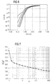
- FIG. 5 shows an input characteristic field of a P-channel transistor which was recorded directly after the P-channel transistor was manufactured.
- the five characteristic curves shown belong to different source-drain voltages, whereby the lowest characteristic curve can be assigned to the lowest source-drain voltage and the top characteristic curve to the highest source-drain voltage. It can be seen that the transistor shows good switch-off behavior with 10 -11 amperes even at high source-drain voltages.
- FIG. 6 shows the input characteristic field of the transistor known from FIG. 5 after the burn-in process according to the invention. It can be clearly seen that the switch-off behavior at high source-drain voltages is no longer very good, since source-drain currents of 10 -7 amperes flow, which is a factor 10000 greater than before the burn-in process.
- the principle of operation is that one is in the memory existing frequency the transistors of the circuit on and turns off.
- the transistors have gate and drain connections thereby via contacts with that generated on the memory chip and connected to the frequency clocked voltage.
Landscapes
- Dram (AREA)
- Tests Of Electronic Circuits (AREA)
- For Increasing The Reliability Of Semiconductor Memories (AREA)
- Testing Of Individual Semiconductor Devices (AREA)
Abstract
Description
Verfahren zur Durchführung eines Burn-in-Prozesses zum elektrischen Stressen eines HalbleiterspeichersProcess for carrying out a burn-in process for electrical Stressing a semiconductor memory
Die Erfindung betrifft ein Verfahren zur Durchführung eines Burn-in-Prozesses zum elektrischen Stressen eines Halbleiterspeichers.The invention relates to a method for carrying out a Burn-in process for the electrical stressing of a semiconductor memory.
Halbleiterspeicher werden zur Informationsspeicherung verwendet und können als Halbleiterbauelement realisiert werden. Ein Halbleiterspeicher ist z.B. ein DRAM (Dynamic Random Access Memory). Es umfaßt aus einem Zellenfeld mit Speicherzellen und einer Ansteuerungsperipherie. Die Speicherzellen des Speicherzellenfeldes bestehen aus einem Auswahltransistor und einem Speicherkondensator. Die Ansteuerungsperipherie wird üblicherweise aus Transistoren gebildet, die in CMOS-Technologie gefertigt sind. CMOS bedeutet Complementary Metal Oxyd Semiconductor und enthält sowohl N-MOS- als auch P-MOS-Transistoren verwendet werden.Semiconductor memories are used for information storage and can be implemented as a semiconductor device. A semiconductor memory is e.g. a DRAM (Dynamic Random Access memory). It comprises a cell array with memory cells and a control periphery. The memory cells of the memory cell array consist of a selection transistor and a storage capacitor. The control periphery is usually formed from transistors using CMOS technology are made. CMOS means Complementary Metal Oxyd Semiconductor and contains both N-MOS and P-MOS transistors be used.
Um über die gesamte Lebenszeit eines Speicherproduktes eine hohe Zuverlässigkeit der verwendeten Transistoren zu gewährleisten, wird ein Burn-in-Prozeß durchgeführt. Transistoren sind herstellungsbedingt nicht in der Lage, während ihrer gesamten Lebenszeit ein identisches Verhalten beizubehalten, was sich in einer über die Zeit veränderten Eingangs- und Ausgangskennlinie widerspiegelt. Die Veränderung der Transistoren wird z.B. durch sogenannte Hot Carrier Injection (Injektion von hochenergetischen Ladungsträgern) bewirkt, was sich bei Transistoren mit kurzer Kanallänge in immer stärkerem Maße auswirkt. Die Einsatzspannung eines frisch produzierten Transistors ist nicht stabil, da hochenergetische Ladungsträger in dem Gate-Oxid akkumuliert werden. Die Einführung eines Burn-in-Prozesses ermöglicht die Stabilisierung der Transistoreigenschaften auf einen konstanten Wert. Diese Stabilisierung wird während der Burn-in-Phase durchgeführt, während sich der Speicher in einer Testumgebung befindet, so daß Der Baustein im Betrieb stabile Eigenschaften aufweist. Üblicherweise werden die Burn-in-Prozesse in einem Ofen durchgeführt, in dem die Speicher einer erhöhten Temperatur ausgesetzt werden. Druckschriften, in denen die Durchführung eines Burn-in beschrieben wird, sind die Patente US 5,976,899; US 5,917,765; US 5,898,186; US 5,748,543; US 5,636,171; US 6,018,485. Zwei Druckschriften, die Schaltkreise zum Durchführen eines Burn-in beschreiben, sind die Patentschriften US 5,986,917 und US 5,424,990. Weitere Erkenntnisse zum Stressen von MOS-Transistoren sind in Zhi Chen et. al. "On the Mechanism for Interface Trap Generation in MOS Transistors Due to Channel Hot Carrier Stressing", IEEE Electron Device Letters, Vol. 21, No. 1, January 2000, p. 24.In order to achieve a to ensure high reliability of the transistors used, a burn-in process is carried out. Transistors are unable due to manufacturing conditions throughout their To maintain identical behavior throughout life what changes in an input and Output characteristic curve reflects. The change in transistors e.g. by so-called hot carrier injection of high-energy charge carriers) causes what transistors with a short channel length are becoming increasingly stronger Dimensions. The operating voltage of a freshly produced Transistor is not stable because of high energy charge carriers can be accumulated in the gate oxide. The introduction a burn-in process enables stabilization the transistor properties to a constant value. This Stabilization is done during the burn-in phase, while the memory is in a test environment, so that the block has stable properties in operation. The burn-in processes are usually carried out in an oven carried out in which the store has an elevated temperature get abandoned. Publications in which the implementation of a burn-in are the patents US 5,976,899; US 5,917,765; US 5,898,186; US 5,748,543; US 5,636,171; US 6,018,485. Two publications, the circuits to perform a burn-in are the US 5,986,917 and US 5,424,990. More insights for stressing MOS transistors are in Zhi Chen et. al. "On the Mechanism for Interface Trap Generation in MOS Transistors Due to Channel Hot Carrier Stressing ", IEEE Electron Device Letters, Vol. 21, No. January 1, 2000, p. 24th
Es ist die Aufgabe der Erfindung ein Verfahren anzugeben, das bei einem Speicher einen Burn-in-Prozeß durchführt und die elektrische Charakteristik des Speichers stabilisiert.It is the object of the invention to specify a method which performs a burn-in process at a memory and the electrical characteristics of the memory stabilized.
Erfindungsgemäß wird die Aufgabe durch ein Verfahren zur Durchführung eines Burn-in-Prozesses zum elektrischen Stressen eines Halbleiterspeichers mit den Schritten:
- Bereitstellen eines Speichers, der eine Schaltungsanordnung mit einem ersten Spannungsanschluß und einem zweiten Spannungsanschluß und einem Steuereingang aufweist, wobei die Schaltungsanordnung einen MOS-Transistor umfaßt;
- Anlegen eines Bezugspotentials an den ersten Spannungsanschluß;
- Anlegen einer zweiten Spannung an den zweiten Spannungsanschluß;
- Anlegen einer Steuerspannung an den Steuereingang, wobei die Steuerspannung variiert wird.
- Providing a memory having a circuit arrangement with a first voltage connection and a second voltage connection and a control input, the circuit arrangement comprising a MOS transistor;
- Applying a reference potential to the first voltage connection;
- Applying a second voltage to the second voltage terminal;
- Applying a control voltage to the control input, the control voltage being varied.
Der Mechanismus, auf dem der erfindungsgemäße Burn-in-Prozeß beruht, ist dynamisches Stressen eines MOS-Transistors. Um einen MOS-Transistor zu stressen, wird z.B. sein Source-Anschluß an ein Bezugspotential, sein Drain-Anschluß an eine Betriebsspannung und sein Gate-Anschluß an eine alternierende Spannung angelegt, die Werte zwischen dem Bezugspotential und der Betriebsspannung annimmt. Die Spannung am Drain-Anschluß wird z.B. größer gewählt, als die Spannung am Gate-Anschluß. Die Eigenschaften eines Transistors verändern sich unter diesen Streßbedingungen in wenigen Stunden so sehr, wie bei normalem Betrieb in zwei Jahren. Dadurch stabilisiert sich seine Eingangsspannung und bleibt während seiner erwarteten zehnjährigen Betriebszeit beim Kunden bei normalem Betrieb in dem Speicher konstant. Vorteilhafterweise kann ein durch den Streß veränderter Transistor in der Speicherschaltungsperipherie bereits während der Testphase identifiziert werden, so daß der defekte Speicher nicht als Produkt ausgeliefert wird. Unter Einwirkung von Streß wird beispielsweise die Einsatzspannung des Transistors verändert und stabilisiert sich. In der Schaltungsperipherie sind kombinatorische Blöcke angeordnet, die Transistoren enthalten.The mechanism on which the burn-in process according to the invention is dynamic stressing of a MOS transistor. Around Stressing a MOS transistor is e.g. its source connector to a reference potential, its drain connection to a Operating voltage and its gate connection to an alternating Voltage applied, the values between the reference potential and of the operating voltage. The voltage at the drain connection e.g. chosen greater than the voltage at the gate connection. The properties of a transistor change among them Stress conditions in a few hours as much as normal ones Operation in two years. This stabilizes his Input voltage and remains during its expected ten-year period Operating time at the customer during normal operation in the Memory constant. Advantageously, a through the Stress modified transistor in the memory circuit periphery be identified during the test phase, so that the defective memory is not delivered as a product. Under stress, for example, the threshold voltage of the transistor changes and stabilizes. In combinatorial blocks are arranged in the circuit periphery, which contain transistors.
In einer Weiterbildung des erfindungsgemäßen Verfahrens nimmt die Steuerspannung Spannungswerte an, die zwischen dem Bezugspotential und einer Betriebsspannung alternieren. Durch dieses Vorgehen wird eine beschleunigte Alterung der Schaltungsanordnung erreicht.In a further development of the method according to the invention the control voltage voltage values between the reference potential and an operating voltage alternate. By this procedure will accelerate the aging of the circuit arrangement reached.
Eine weitere Ausbildung des erfindungsgemäßen Verfahrens sieht vor, daß die Schaltungsanordnung einen Inverter enthält, wobei an einen Invertereingang die Steuerspannung, an eine erste Inverterspannungsversorgung das Bezugspotential und an eine zweite Inverterspannungsversorgung die zweite Spannung angelegt wird. Durch diese Anordnung wird erreicht, daß ein zu stressender Transistor in der Schaltungsanordnung angeordnet ist. Darüber hinaus ist vorgesehen, daß die Schaltungsanordnung einen Inverter enthält. Ein Inverter ist das Basiselement einer jeden CMOS-Schaltung und ist auch in der Schaltungsperipherie eines Speichers enthalten. Weiterhin sind in den Schaltungsblöcken logische Funktionen wie AND, NAND, OR, NOR, XOR etc. enthalten. Another embodiment of the method according to the invention provides that the circuit arrangement contains an inverter, the control voltage being applied to an inverter input a first inverter voltage supply the reference potential and the second to a second inverter voltage supply Voltage is applied. This arrangement achieves that a stressful transistor in the circuit arrangement is arranged. In addition, it is provided that the circuit arrangement contains an inverter. It is an inverter Basic element of every CMOS circuit and is also in the Circuit periphery of a memory included. Farther are logic functions such as AND in the circuit blocks, NAND, OR, NOR, XOR etc. included.
In einer Weiterbildung des erfindungsgemäßen Verfahrens nimmt die zweite Spannung den Wert der Betriebsspannung an. Durch diese Anordnung fällt über der Schaltungsanordnung die Spannungsdifferenz zwischen Bezugspotential und Betriebsspannung ab.In a further development of the method according to the invention the second voltage indicates the value of the operating voltage. By this arrangement drops the voltage difference across the circuit arrangement between reference potential and operating voltage from.
Eine vorteilhafte Ausprägung des erfindungsgemäßen Verfahrens sieht vor, daß die an dem zweiten Spannungsanschluß anliegende zweite Spannung zwischen dem Bezugspotential und der Betriebsspannung alterniert. Durch das Alternieren der zweiten Spannung wird der Streß für die Schaltungsanordnung erhöht, so daß die Zeit zum Stressen reduziert werden kann und der gleiche Streßeffekt in kürzerer Zeit erzielt wird.An advantageous embodiment of the method according to the invention provides that the applied to the second voltage connection second voltage between the reference potential and the operating voltage alternates. By alternating the second Voltage, the stress for the circuit arrangement is increased, so that the time to stress can be reduced and the same stress effect is achieved in less time.
Eine Weiterbildung des erfindungsgemäßen Verfahrens sieht vor, daß die zweite Spannung mit einer ersten Frequenz und die Steuerspannung mit einer zweiten Frequenz zwischen dem Bezugspotential und der Betriebsspannung alternieren. Das periodische Alternieren der zweiten Spannung und der Steuerspannung mit jeweils einer festen Frequenz ermöglicht eine einfache schaltungstechnische Realisierung einer Anordnung zur Durchführung eines Burn-in-Prozesses.A further development of the method according to the invention provides before that the second voltage at a first frequency and the control voltage with a second frequency between the Alternate reference potential and operating voltage. The periodic Alternating the second voltage and the control voltage each with a fixed frequency enables simple circuit implementation of an arrangement to carry out a burn-in process.
Eine vorteilhafte Ausbildung des erfindungsgemäßen Verfahrens sieht vor, daß die erste Frequenz gleich der zweiten Frequenz ist, und die beiden Spannungen eine Phasendifferenz zwischen 150 bis 210 Grad aufweisen. Eine Phasendifferenz von 180 Grad bedeutet, daß sich die beiden Signale genau gegenphasig verhalten. Der Toleranzbereich zwischen 150 bis 210 Grad Phasenverschiebung ermöglicht eine Variation der Phasenverschiebung in dem angegebenen Bereich, was verschiedenste Streßkonstellationen für die Schaltungsanordnung bedeutet.An advantageous embodiment of the method according to the invention stipulates that the first frequency be equal to the second frequency is, and the two voltages have a phase difference between Have 150 to 210 degrees. A phase difference of 180 degrees means that the two signals behave exactly in phase opposition. The tolerance range between 150 to 210 degrees phase shift enables a variation of the phase shift in the specified range, what a variety of stress constellations means for the circuit arrangement.
Eine weitere vorteilhafte Ausbildung des erfindungsgemäßen Verfahrens sieht vor, daß die Phasendifferenz variiert wird. Durch die Variation der Phasendifferenz kann eine Vielfalt von Konstellationen der Betriebsspannung und Steuerspannung erzeugt werden. Dadurch wird der Streß der Schaltungsanordnung weiter erhöht, was die Zeit für den Burn-in-Prozesses vermindert.Another advantageous embodiment of the invention The method provides that the phase difference is varied. By varying the phase difference there can be a variety of constellations of the operating voltage and control voltage be generated. This will stress the circuitry further increases what the time for the burn-in process reduced.
Weitere Ausführungsbeispiele der Erfindung sind in den Unteransprüchen angegeben.Further embodiments of the invention are in the subclaims specified.
Die Erfindung wird nachfolgend anhand eines Ausführungsbeispiels und anhand von Zeichnungen näher erläutert.The invention is described below using an exemplary embodiment and explained in more detail with reference to drawings.
In den Figuren zeigen:
Figur 1- ein Diagramm mit einem erfindungsgemäßen Spannungsverlauf;
Figur 2- ein weiteres Diagramm mit einem erfindungsgemäßen Spannungsverlauf;
- Figur 3
- ein weiteres Diagramm mit einem erfindungsgemäßen Spannungsverlauf;
Figur 4- eine Schaltungsanordnung mit Spannungsversorgungsanschlüssen;
Figur 5- ein Eingangskennlinienfeld eines P-Kanal-Transistors, bevor er gestreßt wurde;
Figur 6- das Eingangskennlinienfeld eines P-Kanal-Transistors, nachdem er gestreßt wurde;
- Figur 7
- die Veränderung der Einsatzspannung unter Einwirkung von Streß über der Zeit.
- Figure 1
- a diagram with a voltage curve according to the invention;
- Figure 2
- another diagram with a voltage curve according to the invention;
- Figure 3
- another diagram with a voltage curve according to the invention;
- Figure 4
- a circuit arrangement with voltage supply connections;
- Figure 5
- an input map of a P-channel transistor before it has been stressed;
- Figure 6
- the input characteristic field of a P-channel transistor after it has been stressed;
- Figure 7
- the change in the threshold voltage under the influence of stress over time.
In Figur 4 ist eine Schaltungsanordnung 1 mit einem ersten
Spannungsanschluß 2 einem zweiten Spannungsanschluß 3 und einem
Steuereingang 4 dargestellt. In der Schaltungsanordnung 1
befindet sich ein logischer Block, der z.B. ein MOS-Transistor
oder einen CMOS-Inverter enthält. Im folgenden
werden Spannungsverläufe beschrieben, die dazu geeignet sind,
die Schaltungsanordnung 1 zu stressen und so vorzeitig altern
zu lassen, damit die Schaltungsanordnung 1 ein konstantes
Verhalten annimmt.In Figure 4 is a
In Figur 1 ist auf der Abszisse die Zeit und auf der Ordinate
die Spannung dargestellt. Weiterhin ist der Verlauf eines Bezugspotentials
5, der Verlauf einer Betriebsspannung 8, der
Verlauf einer zweiten Spannung 6, die mit dem Verlauf der Betriebsspannung
identisch ist und der Verlauf einer Steuerspannung
7 dargestellt. Die Steuerspannung 7 alterniert in
diesem Ausführungsbeispiel zwischen dem Bezugspotential 5 und
der Betriebsspannung 8. Um die Schaltungsanordnung 1 mit dem
Spannungsverlauf aus Figur 1 zu stressen, wird beispielsweise
der erste Spannungsanschluß 2 an das Bezugspotential 5, der
zweite Spannungsanschluß 3 an die zweite Spannung 6 und der
Steuereingang 4 an die Steuerspannung 7 angeschlossen. Üblicherweise
wird die Größe der Spannungen so gewählt, daß die
von der Schaltungsanordnung 1 umfaßten Bauelemente einen Alterungsprozeß
erfahren, allerdings nicht direkt durch Überspannungen
zerstört werden.In Figure 1, the time is on the abscissa and the ordinate
the tension shown. Furthermore, the course of a
In Figur 2 ist ein weiteres Ausführungsbeispiel eines erfindungsgemäßen
Spannungsverlaufs dargestellt. Der Unterschied
zu Figur 1 besteht darin, daß in Figur 2 die zweite Spannung
6 nicht konstant auf dem Wert der Betriebsspannung 8 gehalten
wird, sondern zwischen dem Bezugspotential 5 und der Betriebsspannung
8 alterniert. Dabei oszilliert die zweite
Spannung 6 mit einer ersten Frequenz 9 und die Steuerspannung
7 mit einer zweiten Frequenz 10. In diesem Ausführungsbeispiel
sind die beiden Frequenzen identisch, die entsprechenden
Spannungen weisen allerdings eine Phasenverschiebung von
etwa 180 Grad auf. Dadurch erreicht die zweite Spannung einen
hohen Spannungswert, wenn die Steuerspannung einen niedrigen
Spannungswert annimmt, und umgekehrt. Durch dieses Vorgehen
wird die Schaltungsanordnung 1 in ihrem Alterungsprozeß beschleunigt.In Figure 2 is another embodiment of an inventive
Voltage curve shown. The difference
to Figure 1 is that in Figure 2, the
In Figur 3 ist ein weiteres Ausführungsbeispiel eines erfindungsgemäßen
Spannungsverlaufs dargestellt. Im Gegensatz zu
Figur 2 ist in Figur 3 die Phasenlage der zweiten Spannung 6
und der Steuerspannung 7 nicht konstant bei 180 Grad, sondern
kann in einem Bereich von ± 30 Grad variiert werden. Durch
die Variation der Phasenlage wird der Streß auf die Schaltungsanordnung
1 weiter erhöht, so daß die zur beschleunigten
Alterung (Burn-in) der Schaltungsanordnung 1 benötigte Zeit
in vorteilhafter Weise reduziert werden kann.In Figure 3 is another embodiment of an inventive
Voltage curve shown. In contrast to
FIG. 2 is the phase position of the
Figur 5 zeigt ein Eingangskennlinienfeld eines P-Kanal-Transistors, welches direkt nach der Herstellung des P-Kanal-Transistors aufgenommen worden ist. Die fünf dargestellten Kennlinien gehören zu unterschiedlichen Source-Drain-Spannungen, wobei die unterste Kennlinie der niedrigsten Source-Drain-Spannung und die oberste Kennlinie der höchsten Source-Drain-Spannung zugeordnet werden kann. Es ist zu erkennen, daß der Transistor auch bei hohen Source-Drain-Spannungen ein gutes Abschaltverhalten mit 10-11 Ampere zeigt.FIG. 5 shows an input characteristic field of a P-channel transistor which was recorded directly after the P-channel transistor was manufactured. The five characteristic curves shown belong to different source-drain voltages, whereby the lowest characteristic curve can be assigned to the lowest source-drain voltage and the top characteristic curve to the highest source-drain voltage. It can be seen that the transistor shows good switch-off behavior with 10 -11 amperes even at high source-drain voltages.
In Figur 6 ist das Eingangskennlinienfeld des aus Figur 5 bekannten Transistors nach dem erfindungsgemäßen Burn-in-Prozeß dargestellt. Deutlich ist zu erkennen, daß das Abschaltverhalten bei hohen Source-Drain-Spannungen nicht mehr sehr gut ist, da Source-Drain-Ströme von 10-7 Ampere fließen, was einen Faktor 10000 größer ist als vor dem Burn-in-Prozeß.FIG. 6 shows the input characteristic field of the transistor known from FIG. 5 after the burn-in process according to the invention. It can be clearly seen that the switch-off behavior at high source-drain voltages is no longer very good, since source-drain currents of 10 -7 amperes flow, which is a factor 10000 greater than before the burn-in process.
Mit Bezug auf Figur 7 ist die Variation der Einsatzspannung über der Zeit dargestellt. Deutlich ist zu erkennen, daß die Einsatzspannung im Laufe der Zeit abnimmt und sich stabilisiert.With reference to Figure 7 is the variation in threshold voltage represented over time. It can be clearly seen that the Tension decreases over time and stabilizes.
Das Funktionsprinzip besteht darin, daß eine in dem Speicher vorhandene Frequenz die Transistoren der Schaltung ein- und ausschaltet. Gate- und Drain-Anschlüsse der Transistoren sind dabei über Kontakte mit der auf dem Speicherchip erzeugten und mit der Frequenz getakteten Spannung verbunden.The principle of operation is that one is in the memory existing frequency the transistors of the circuit on and turns off. The transistors have gate and drain connections thereby via contacts with that generated on the memory chip and connected to the frequency clocked voltage.
Weiterhin ist es vorteilhaft, einen Temperaturgradienten während der elektrischen Streßphase an den Speicher anzulegen, um die Streßphase zu verkürzen. It is also advantageous to maintain a temperature gradient during the electrical stress phase to apply to the memory, to shorten the stress phase.
- 11
- SchaltungsanordnungCircuit arrangement
- 22nd
- erster Spannungsanschlußfirst voltage connection
- 33rd
- zweiter Spannungsanschlußsecond voltage connection
- 44th
- SteuereingangControl input
- 55
- BezugspotentialReference potential
- 66
- zweite Spannungsecond tension
- 77
- SteuerspannungControl voltage
- 88th
- BetriebsspannungOperating voltage
- 99
- erste Frequenzfirst frequency
- 1010th
- zweite Frequenzsecond frequency
- 1111
- erste Phasenverschiebungfirst phase shift
- 1212th
- zweite Phasenverschiebungsecond phase shift
Claims (8)
dadurch gekennzeichnet, daß
die Steuerspannung (7) Spannungswerte annimmt, die zwischen dem Bezugspotential (5) und einer Betriebsspannung (8) alternieren.Method according to claim 1,
characterized in that
the control voltage (7) assumes voltage values that alternate between the reference potential (5) and an operating voltage (8).
dadurch gekennzeichnet, daß
die Schaltungsanordnung (1) einen Inverter enthält, wobei an einen Invertereingang die Steuerspannung (7), an eine erste Inverterspannungsversorgung das Bezugspotential (5) und an eine zweite Inverterspannungsversorgung die zweite Spannung (6) angelegt wird.The method of claim 1 or 2,
characterized in that
the circuit arrangement (1) contains an inverter, the control voltage (7) being applied to an inverter input, the reference potential (5) being applied to a first inverter voltage supply and the second voltage (6) being applied to a second inverter voltage supply.
dadurch gekennzeichnet, daß
die zweite Spannung (6) den Wert der Betriebsspannung (8) annimmt. Method according to one of claims 1 to 3,
characterized in that
the second voltage (6) assumes the value of the operating voltage (8).
dadurch gekennzeichnet, daß
die an dem zweiten Spannungsanschluß (3) anliegende zweite Spannung (6) zwischen dem Bezugspotential (5) und der Betriebsspannung (8) alterniert.Method according to one of claims 1 to 3,
characterized in that
the second voltage (6) present at the second voltage connection (3) alternates between the reference potential (5) and the operating voltage (8).
dadurch gekennzeichnet, daß
die zweite Spannung (6) mit einer ersten Frequenz (9) und die Steuerspannung (7) mit einer zweiten Frequenz (10) zwischen dem Bezugspotential (5) und der Betriebsspannung (8) alternieren.Method according to one of claims 1 to 5,
characterized in that
the second voltage (6) with a first frequency (9) and the control voltage (7) with a second frequency (10) alternate between the reference potential (5) and the operating voltage (8).
dadurch gekennzeichnet, daß
die erste Frequenz (9) gleich der zweiten Frequenz (10) ist, und die beiden Spannungen (6,7) eine Phasendifferenz zwischen 150 bis 210 Grad aufweisen.Method according to one of claims 1 to 6,
characterized in that
the first frequency (9) is equal to the second frequency (10), and the two voltages (6,7) have a phase difference between 150 to 210 degrees.
dadurch gekennzeichnet, daß
die Phasendifferenz (11) variiert wird.Method according to claim 7,
characterized in that
the phase difference (11) is varied.
Applications Claiming Priority (2)
| Application Number | Priority Date | Filing Date | Title |
|---|---|---|---|
| DE10014388 | 2000-03-23 | ||
| DE10014388A DE10014388A1 (en) | 2000-03-23 | 2000-03-23 | Conducting memory device burn-in process enabling electrical characteristics of memory device to be stabilised - involves applying reference potential, second voltage to voltage connections, varying control voltage between reference potential and operating voltage |
Publications (2)
| Publication Number | Publication Date |
|---|---|
| EP1136833A1 true EP1136833A1 (en) | 2001-09-26 |
| EP1136833B1 EP1136833B1 (en) | 2005-01-26 |
Family
ID=7636020
Family Applications (1)
| Application Number | Title | Priority Date | Filing Date |
|---|---|---|---|
| EP01104285A Expired - Lifetime EP1136833B1 (en) | 2000-03-23 | 2001-02-22 | Method of performing a burn-in process to electrically stress a semiconductor memory |
Country Status (4)
| Country | Link |
|---|---|
| US (1) | US6445630B2 (en) |
| EP (1) | EP1136833B1 (en) |
| DE (2) | DE10014388A1 (en) |
| TW (1) | TW525179B (en) |
Families Citing this family (10)
| Publication number | Priority date | Publication date | Assignee | Title |
|---|---|---|---|---|
| US6891404B2 (en) * | 2002-06-11 | 2005-05-10 | Infineon Technologies | Auto-adjustment of self-refresh frequency |
| US6969618B2 (en) * | 2002-08-23 | 2005-11-29 | Micron Technology, Inc. | SOI device having increased reliability and reduced free floating body effects |
| EP3308744B2 (en) | 2004-03-11 | 2023-08-02 | Percutaneous Cardiovascular Solutions Pty Limited | Percutaneous heart valve prosthesis |
| US20060169281A1 (en) * | 2005-02-03 | 2006-08-03 | Aylsworth Alonzo C | Continuous flow selective delivery of therapeutic gas |
| WO2010057262A1 (en) | 2008-11-21 | 2010-05-27 | Percutaneous Cardiovascular Solutions Pty Limited | Heart valve prosthesis and method |
| JP6179158B2 (en) * | 2013-03-27 | 2017-08-16 | 三菱電機株式会社 | Transistor manufacturing method and amplifier manufacturing method |
| RU2554660C1 (en) * | 2013-12-06 | 2015-06-27 | Максимов Владимир Алексеевич | Burn-in test method for integrated microcircuits |
| JP6292104B2 (en) * | 2014-11-17 | 2018-03-14 | 三菱電機株式会社 | Manufacturing method of nitride semiconductor device |
| US11115022B2 (en) * | 2015-05-07 | 2021-09-07 | Northwestern University | System and method for integrated circuit usage tracking circuit with fast tracking time for hardware security and re-configurability |
| CN107202946B (en) * | 2017-05-22 | 2019-07-02 | 西安电子科技大学 | Method of Measuring MOS Threshold Voltage of CMOS Inverter |
Citations (5)
| Publication number | Priority date | Publication date | Assignee | Title |
|---|---|---|---|---|
| WO1982000917A1 (en) * | 1980-09-08 | 1982-03-18 | Proebsting R | Tape burn-in circuit |
| US5557559A (en) * | 1992-07-06 | 1996-09-17 | Motay Electronics, Inc. | Universal burn-in driver system and method therefor |
| DE19603107A1 (en) * | 1995-12-26 | 1997-07-03 | Lg Semicon Co Ltd | Self pre-ageing circuit device for semiconductor memory e.g. application specific memory |
| US5872797A (en) * | 1996-12-02 | 1999-02-16 | International Business Machines Corporation | Burn-in signal pattern generator |
| US6038181A (en) * | 1998-08-18 | 2000-03-14 | Internatioal Business Machines Corp. | Efficient semiconductor burn-in circuit and method of operation |
Family Cites Families (9)
| Publication number | Priority date | Publication date | Assignee | Title |
|---|---|---|---|---|
| US4751679A (en) * | 1986-12-22 | 1988-06-14 | Motorola, Inc. | Gate stress test of a MOS memory |
| KR950014099B1 (en) * | 1992-06-12 | 1995-11-21 | 가부시기가이샤 도시바 | Semiconductor memory device |
| JP2885597B2 (en) | 1993-03-10 | 1999-04-26 | 株式会社東芝 | Semiconductor memory |
| KR0122107B1 (en) | 1994-06-04 | 1997-12-05 | 김광호 | Semiconductor memory device with low power cell refresh and burn-in |
| KR970001564U (en) | 1995-06-21 | 1997-01-21 | Reinforcement Structure of Automobile Rear Body | |
| US5898186A (en) | 1996-09-13 | 1999-04-27 | Micron Technology, Inc. | Reduced terminal testing system |
| KR100228530B1 (en) | 1996-12-23 | 1999-11-01 | 윤종용 | Wafer burn-in test circuit for semiconductor memory device |
| JP4046382B2 (en) | 1997-03-27 | 2008-02-13 | 株式会社ルネサステクノロジ | Semiconductor integrated circuit device |
| KR100268434B1 (en) | 1997-12-29 | 2000-10-16 | 윤종용 | Semiconductor memory device and burn-in test method thereof |
-
2000
- 2000-03-23 DE DE10014388A patent/DE10014388A1/en not_active Withdrawn
-
2001
- 2001-02-22 EP EP01104285A patent/EP1136833B1/en not_active Expired - Lifetime
- 2001-02-22 DE DE50105160T patent/DE50105160D1/en not_active Expired - Lifetime
- 2001-03-22 TW TW090106783A patent/TW525179B/en not_active IP Right Cessation
- 2001-03-23 US US09/816,924 patent/US6445630B2/en not_active Expired - Lifetime
Patent Citations (5)
| Publication number | Priority date | Publication date | Assignee | Title |
|---|---|---|---|---|
| WO1982000917A1 (en) * | 1980-09-08 | 1982-03-18 | Proebsting R | Tape burn-in circuit |
| US5557559A (en) * | 1992-07-06 | 1996-09-17 | Motay Electronics, Inc. | Universal burn-in driver system and method therefor |
| DE19603107A1 (en) * | 1995-12-26 | 1997-07-03 | Lg Semicon Co Ltd | Self pre-ageing circuit device for semiconductor memory e.g. application specific memory |
| US5872797A (en) * | 1996-12-02 | 1999-02-16 | International Business Machines Corporation | Burn-in signal pattern generator |
| US6038181A (en) * | 1998-08-18 | 2000-03-14 | Internatioal Business Machines Corp. | Efficient semiconductor burn-in circuit and method of operation |
Also Published As
| Publication number | Publication date |
|---|---|
| DE10014388A1 (en) | 2001-10-04 |
| US6445630B2 (en) | 2002-09-03 |
| DE50105160D1 (en) | 2005-03-03 |
| EP1136833B1 (en) | 2005-01-26 |
| TW525179B (en) | 2003-03-21 |
| US20010033518A1 (en) | 2001-10-25 |
Similar Documents
| Publication | Publication Date | Title |
|---|---|---|
| DE3032657C2 (en) | ||
| DE3041176A1 (en) | SEMICONDUCTOR STORAGE DEVICE | |
| DE19603447C2 (en) | Semiconductor integrated circuit device | |
| EP1136833B1 (en) | Method of performing a burn-in process to electrically stress a semiconductor memory | |
| WO2007118679A1 (en) | Circuit arrangement comprising a non-volatile memory cell, and method | |
| DE102005061375B4 (en) | NOR flash memory device with multi-level memory cell and bit value detection method | |
| DE19622646B4 (en) | Integrated semiconductor circuit device | |
| DE69329543T2 (en) | Manufacture of a field effect transistor with an integrated Schottky clamping diode | |
| DE3722421C2 (en) | ||
| DE19934297C1 (en) | Semiconductor integrated circuit with NMOS transistors | |
| EP1153394B1 (en) | Method for operating a memory cell array with self-amplifying dynamic memory cells | |
| DE2749711A1 (en) | METHOD AND ARRANGEMENT FOR INFLUENCING AND DETECTING CARGO CARRIAGE INJECTION PROCESSES IN FIELD EFFECT COMPONENTS | |
| EP0045403B1 (en) | Method of producing a device to reduce the influence of radiation on mos memory cells | |
| DE4336883A1 (en) | Integrated circuit output driver for suppressing noise generation, e.g. in DRAM - has current increase rate controller responding to voltage at predefined node in semiconductor substrate | |
| DE2550276A1 (en) | CAPACITIVE DATA STORAGE | |
| DE2433077A1 (en) | DYNAMIC STORAGE DEVICE | |
| DE2450882A1 (en) | Logic circuit based on complementary MOS transistors - has two gate stages each with three MOS transistors | |
| DE3032306C2 (en) | ||
| DE102020101267A1 (en) | Balanced negative bit line voltage for a circuit with write support | |
| DE102005009050B4 (en) | Differential readout circuit for fuse memory cells | |
| DE2360887A1 (en) | COMPLEMENTARY STORAGE ELEMENT | |
| DE10344872A1 (en) | Integrated circuit with protection against electrostatic discharge | |
| DE10211932B4 (en) | Circuit arrangement for reading, evaluating and re-reading a state of charge in a memory cell | |
| DE69422220T2 (en) | Output circuit with three supply voltages | |
| DE2261522A1 (en) | SEMI-CONDUCTOR STORAGE UNIT |
Legal Events
| Date | Code | Title | Description |
|---|---|---|---|
| PUAI | Public reference made under article 153(3) epc to a published international application that has entered the european phase |
Free format text: ORIGINAL CODE: 0009012 |
|
| AK | Designated contracting states |
Kind code of ref document: A1 Designated state(s): AT BE CH CY DE DK ES FI FR GB GR IE IT LI LU MC NL PT SE TR Kind code of ref document: A1 Designated state(s): DE FR GB |
|
| AX | Request for extension of the european patent |
Free format text: AL;LT;LV;MK;RO;SI |
|
| 17P | Request for examination filed |
Effective date: 20020326 |
|
| AKX | Designation fees paid |
Free format text: DE FR GB |
|
| 17Q | First examination report despatched |
Effective date: 20030925 |
|
| GRAP | Despatch of communication of intention to grant a patent |
Free format text: ORIGINAL CODE: EPIDOSNIGR1 |
|
| GRAS | Grant fee paid |
Free format text: ORIGINAL CODE: EPIDOSNIGR3 |
|
| GRAA | (expected) grant |
Free format text: ORIGINAL CODE: 0009210 |
|
| AK | Designated contracting states |
Kind code of ref document: B1 Designated state(s): DE FR GB |
|
| REG | Reference to a national code |
Ref country code: GB Ref legal event code: FG4D Free format text: NOT ENGLISH |
|
| REF | Corresponds to: |
Ref document number: 50105160 Country of ref document: DE Date of ref document: 20050303 Kind code of ref document: P |
|
| GBT | Gb: translation of ep patent filed (gb section 77(6)(a)/1977) |
Effective date: 20050413 |
|
| PLBE | No opposition filed within time limit |
Free format text: ORIGINAL CODE: 0009261 |
|
| STAA | Information on the status of an ep patent application or granted ep patent |
Free format text: STATUS: NO OPPOSITION FILED WITHIN TIME LIMIT |
|
| ET | Fr: translation filed | ||
| 26N | No opposition filed |
Effective date: 20051027 |
|
| PGFP | Annual fee paid to national office [announced via postgrant information from national office to epo] |
Ref country code: GB Payment date: 20070216 Year of fee payment: 7 |
|
| PGFP | Annual fee paid to national office [announced via postgrant information from national office to epo] |
Ref country code: FR Payment date: 20080214 Year of fee payment: 8 |
|
| GBPC | Gb: european patent ceased through non-payment of renewal fee |
Effective date: 20080222 |
|
| PG25 | Lapsed in a contracting state [announced via postgrant information from national office to epo] |
Ref country code: GB Free format text: LAPSE BECAUSE OF NON-PAYMENT OF DUE FEES Effective date: 20080222 |
|
| REG | Reference to a national code |
Ref country code: FR Ref legal event code: ST Effective date: 20091030 |
|
| PG25 | Lapsed in a contracting state [announced via postgrant information from national office to epo] |
Ref country code: FR Free format text: LAPSE BECAUSE OF NON-PAYMENT OF DUE FEES Effective date: 20090302 |
|
| REG | Reference to a national code |
Ref country code: DE Ref legal event code: R081 Ref document number: 50105160 Country of ref document: DE Owner name: INFINEON TECHNOLOGIES AG, DE Free format text: FORMER OWNER: QIMONDA AG, 81739 MUENCHEN, DE Ref country code: DE Ref legal event code: R081 Ref document number: 50105160 Country of ref document: DE Owner name: POLARIS INNOVATIONS LTD., IE Free format text: FORMER OWNER: QIMONDA AG, 81739 MUENCHEN, DE |
|
| PGFP | Annual fee paid to national office [announced via postgrant information from national office to epo] |
Ref country code: DE Payment date: 20150414 Year of fee payment: 15 |
|
| REG | Reference to a national code |
Ref country code: DE Ref legal event code: R081 Ref document number: 50105160 Country of ref document: DE Owner name: POLARIS INNOVATIONS LTD., IE Free format text: FORMER OWNER: INFINEON TECHNOLOGIES AG, 85579 NEUBIBERG, DE |
|
| REG | Reference to a national code |
Ref country code: DE Ref legal event code: R119 Ref document number: 50105160 Country of ref document: DE |
|
| PG25 | Lapsed in a contracting state [announced via postgrant information from national office to epo] |
Ref country code: DE Free format text: LAPSE BECAUSE OF NON-PAYMENT OF DUE FEES Effective date: 20160901 |