EP1136588A2 - Méthode MOCVD d'un film d'oxyde de tantale - Google Patents
Méthode MOCVD d'un film d'oxyde de tantale Download PDFInfo
- Publication number
- EP1136588A2 EP1136588A2 EP01106421A EP01106421A EP1136588A2 EP 1136588 A2 EP1136588 A2 EP 1136588A2 EP 01106421 A EP01106421 A EP 01106421A EP 01106421 A EP01106421 A EP 01106421A EP 1136588 A2 EP1136588 A2 EP 1136588A2
- Authority
- EP
- European Patent Office
- Prior art keywords
- process container
- target substrate
- materials
- tantalum oxide
- oxidizing agent
- Prior art date
- Legal status (The legal status is an assumption and is not a legal conclusion. Google has not performed a legal analysis and makes no representation as to the accuracy of the status listed.)
- Withdrawn
Links
Images




Classifications
-
- H—ELECTRICITY
- H10—SEMICONDUCTOR DEVICES; ELECTRIC SOLID-STATE DEVICES NOT OTHERWISE PROVIDED FOR
- H10P—GENERIC PROCESSES OR APPARATUS FOR THE MANUFACTURE OR TREATMENT OF DEVICES COVERED BY CLASS H10
- H10P14/00—Formation of materials, e.g. in the shape of layers or pillars
- H10P14/60—Formation of materials, e.g. in the shape of layers or pillars of insulating materials
- H10P14/69—Inorganic materials
- H10P14/692—Inorganic materials composed of oxides, glassy oxides or oxide-based glasses
- H10P14/6938—Inorganic materials composed of oxides, glassy oxides or oxide-based glasses the material containing at least one metal element, e.g. metal oxides, metal oxynitrides or metal oxycarbides
- H10P14/6939—Inorganic materials composed of oxides, glassy oxides or oxide-based glasses the material containing at least one metal element, e.g. metal oxides, metal oxynitrides or metal oxycarbides characterised by the metal
- H10P14/69393—Inorganic materials composed of oxides, glassy oxides or oxide-based glasses the material containing at least one metal element, e.g. metal oxides, metal oxynitrides or metal oxycarbides characterised by the metal the material containing tantalum, e.g. Ta2O5
-
- C—CHEMISTRY; METALLURGY
- C23—COATING METALLIC MATERIAL; COATING MATERIAL WITH METALLIC MATERIAL; CHEMICAL SURFACE TREATMENT; DIFFUSION TREATMENT OF METALLIC MATERIAL; COATING BY VACUUM EVAPORATION, BY SPUTTERING, BY ION IMPLANTATION OR BY CHEMICAL VAPOUR DEPOSITION, IN GENERAL; INHIBITING CORROSION OF METALLIC MATERIAL OR INCRUSTATION IN GENERAL
- C23C—COATING METALLIC MATERIAL; COATING MATERIAL WITH METALLIC MATERIAL; SURFACE TREATMENT OF METALLIC MATERIAL BY DIFFUSION INTO THE SURFACE, BY CHEMICAL CONVERSION OR SUBSTITUTION; COATING BY VACUUM EVAPORATION, BY SPUTTERING, BY ION IMPLANTATION OR BY CHEMICAL VAPOUR DEPOSITION, IN GENERAL
- C23C16/00—Chemical coating by decomposition of gaseous compounds, without leaving reaction products of surface material in the coating, i.e. chemical vapour deposition [CVD] processes
- C23C16/02—Pretreatment of the material to be coated
- C23C16/0272—Deposition of sub-layers, e.g. to promote the adhesion of the main coating
-
- C—CHEMISTRY; METALLURGY
- C23—COATING METALLIC MATERIAL; COATING MATERIAL WITH METALLIC MATERIAL; CHEMICAL SURFACE TREATMENT; DIFFUSION TREATMENT OF METALLIC MATERIAL; COATING BY VACUUM EVAPORATION, BY SPUTTERING, BY ION IMPLANTATION OR BY CHEMICAL VAPOUR DEPOSITION, IN GENERAL; INHIBITING CORROSION OF METALLIC MATERIAL OR INCRUSTATION IN GENERAL
- C23C—COATING METALLIC MATERIAL; COATING MATERIAL WITH METALLIC MATERIAL; SURFACE TREATMENT OF METALLIC MATERIAL BY DIFFUSION INTO THE SURFACE, BY CHEMICAL CONVERSION OR SUBSTITUTION; COATING BY VACUUM EVAPORATION, BY SPUTTERING, BY ION IMPLANTATION OR BY CHEMICAL VAPOUR DEPOSITION, IN GENERAL
- C23C16/00—Chemical coating by decomposition of gaseous compounds, without leaving reaction products of surface material in the coating, i.e. chemical vapour deposition [CVD] processes
- C23C16/06—Chemical coating by decomposition of gaseous compounds, without leaving reaction products of surface material in the coating, i.e. chemical vapour deposition [CVD] processes characterised by the deposition of metallic material
- C23C16/18—Chemical coating by decomposition of gaseous compounds, without leaving reaction products of surface material in the coating, i.e. chemical vapour deposition [CVD] processes characterised by the deposition of metallic material from metallo-organic compounds
-
- C—CHEMISTRY; METALLURGY
- C23—COATING METALLIC MATERIAL; COATING MATERIAL WITH METALLIC MATERIAL; CHEMICAL SURFACE TREATMENT; DIFFUSION TREATMENT OF METALLIC MATERIAL; COATING BY VACUUM EVAPORATION, BY SPUTTERING, BY ION IMPLANTATION OR BY CHEMICAL VAPOUR DEPOSITION, IN GENERAL; INHIBITING CORROSION OF METALLIC MATERIAL OR INCRUSTATION IN GENERAL
- C23C—COATING METALLIC MATERIAL; COATING MATERIAL WITH METALLIC MATERIAL; SURFACE TREATMENT OF METALLIC MATERIAL BY DIFFUSION INTO THE SURFACE, BY CHEMICAL CONVERSION OR SUBSTITUTION; COATING BY VACUUM EVAPORATION, BY SPUTTERING, BY ION IMPLANTATION OR BY CHEMICAL VAPOUR DEPOSITION, IN GENERAL
- C23C16/00—Chemical coating by decomposition of gaseous compounds, without leaving reaction products of surface material in the coating, i.e. chemical vapour deposition [CVD] processes
- C23C16/22—Chemical coating by decomposition of gaseous compounds, without leaving reaction products of surface material in the coating, i.e. chemical vapour deposition [CVD] processes characterised by the deposition of inorganic material, other than metallic material
- C23C16/30—Deposition of compounds, mixtures or solid solutions, e.g. borides, carbides, nitrides
- C23C16/40—Oxides
- C23C16/405—Oxides of refractory metals or yttrium
-
- H—ELECTRICITY
- H10—SEMICONDUCTOR DEVICES; ELECTRIC SOLID-STATE DEVICES NOT OTHERWISE PROVIDED FOR
- H10P—GENERIC PROCESSES OR APPARATUS FOR THE MANUFACTURE OR TREATMENT OF DEVICES COVERED BY CLASS H10
- H10P14/00—Formation of materials, e.g. in the shape of layers or pillars
- H10P14/60—Formation of materials, e.g. in the shape of layers or pillars of insulating materials
- H10P14/63—Formation of materials, e.g. in the shape of layers or pillars of insulating materials characterised by the formation processes
- H10P14/6326—Deposition processes
- H10P14/6328—Deposition from the gas or vapour phase
- H10P14/6334—Deposition from the gas or vapour phase using decomposition or reaction of gaseous or vapour phase compounds, i.e. chemical vapour deposition
Definitions
- the present invention relates to an MOCVD (Metal Organic Chemical Vapor Deposition) method of a tantalum oxide film in a semiconductor processing system, and more specifically to a technique of forming, e.g., a gate insulating film, capacitor insulating, or the like of a semiconductor device.
- MOCVD Metal Organic Chemical Vapor Deposition
- semiconductor process includes various kinds of processes which are performed to manufacture a semiconductor device or a structure having wiring layers, electrodes, and the like to be connected to a semiconductor device, on a target substrate, such as a semiconductor wafer or an LCD (Liquid Crystal Display) substrate, by forming semiconductor layers, insulating layers, and conductive layers in predetermined patterns on the target substrate.
- silicon oxide films and silicon nitride films are used as the insulating films.
- a metal oxide e.g., tantalum oxide (Ta 2 O 5 ).
- the film of this material can be formed by means of MOCVD, i.e., using a vaporized metal organic compound.
- a metal (tantalum) alkoxide such as Ta(OC 2 H 5 ) 5 (pentoethoxytantalum: PET) is used as a raw material liquid.
- the raw material liquid is made to bubble by e.g., nitrogen gas, or vaporized by a vaporizer set at a vaporizing temperature, to be in a gaseous state, and is supplied to a process chamber preset to have a vacuum atmosphere.
- an oxidizing gas such as oxygen, is supplied to the process chamber.
- the supplied raw material is decomposed to offer a film forming material on the surface of a semiconductor wafer heated to a predetermined process temperature. With this film forming material, a tantalum oxide (Ta 2 O 5 ) film is formed on the surface of the semiconductor wafer by means of deposition.
- tantalum oxide films As semiconductor device design rules have become stricter, the required thickness of tantalum oxide films is now about 10 nm at max. Tantalum oxide films grow at a deposition rate of about 150 nm/min when a deposition temperature is about 600°C. Accordingly, where tantalum oxide films having a thickness of about 10 nm have to be formed with high accuracy, a low deposition temperature of about 400°C is used to reduce the deposition rate. In the case of using such conditions for forming tantalum oxide films, however, the present inventors have found a problem in that the surface of the tantalum oxide films becomes uneven, i.e., the degree of surface roughness is higher and the surface morphology is degraded, thereby deteriorating the electric properties of the film.
- An object of the present invention is to provide an MOCVD method, which allows a thin tantalum oxide film to be formed with high controllability in the film thickness, and to have excellent electric properties.
- an MOCVD method of forming a tantalum oxide film on a target substrate in an airtight process container of a semiconductor processing system comprising:
- an MOCVD method of forming a tantalum oxide film on a target substrate in an airtight process container of a semiconductor processing system comprising:
- the oxidizing agent used as one of the third and fourth materials has an oxidizing power lower than that of the oxidizing agent used as one of the first and second materials
- the organic tantalum used as the other of the third and fourth materials is the substantially the same material as the organic tantalum used as the other of the first and second materials
- the target substrate is set at a temperature of from 350 to 500°C in the second layer formation step.
- PET pentoethoxytantalum
- Ta(OC 2 H 5 ) 5 may be used as the organic tantalum.
- the oxidizing agent used as one of the first and second materials may be selected from the group consisting of H 2 O, H 2 O 2 , O 3 , oxygen radical, a mixture of H 2 and O 2 , a mixture of H 2 and N 2 O, a mixture of H 2 and NO, a mixture of NH 3 and O 2 , and a mixture of O 3 and H 2 .
- FIG. 11 is a graph showing the relationship between the deposition rate of tantalum oxide films and an incubation time.
- the incubation time is a period of time at the initial phase of a film formation step, in which no intended film (tantalum oxide film) is deposited even though an organic tantalum gas and an oxidizing gas are supplied.
- the deposition rate of tantalum oxide films and the incubation time are contrary to each other, in terms of the deposition temperature. Specifically, if the deposition temperature is lowered, the deposition rate is reduced to improve the controllability in the film thickness, while the incubation time is increased.
- FIGS. 12A and 12B are sectional views showing steps of a conventional MOCVD method of a tantalum oxide film.
- an underlying layer 6 is disposed on the surface of a semiconductor wafer W of, e.g., silicon.
- the underlying layer 6 consists essentially of any one of silicon oxide (SiOx), silicon nitride (SiNx), and a mixture of them (SiOxNy).
- the underlying layer 6 is used to cause a tantalum oxide film thereon to have an interface level density falling in a certain range and to match with the silicon surface.
- Ta 2 O 5 seeds 14 in an amorphous state are dispersively formed on the surface of the underlying layer 6 of the wafer W, as shown in FIG. 12A.
- a film suddenly starts growing from the seeds 14, and results in a tantalum oxide film 8, as shown in FIG. 12B.
- the tantalum oxide film 8 thus formed has a very uneven surface with projections and recesses, which reflect the projecting state of separated seeds 14. Since the size of the seeds 14 becomes larger essentially in proportion to an increase in the incubation time, a low deposition temperature of about 400°C for forming the tantalum oxide film 8 increases the degree of surface roughness.
- An unevenness of the surface means that the tantalum oxide film 8 has a thicker portion and a thinner portion.
- the thicker portion may have a thickness H1 of about 10 nm, while the thinner portion may have a thickness H2 of about 3 nm.
- an electrical field concentration is caused at the thinner portion, thereby generating a leakage current far lager than the designed value.
- FIGS. 13A, 13B, and 13C are sectional views showing steps of forming the insulating film of tantalum oxide of a capacitor, which has an MIM structure, by a conventional MOCVD method.
- a tantalum oxide film 8 used as a capacitor insulating film is deposited on the lower electrode 3 and the inter-level insulating film 5.
- the tantalum oxide film 8 is formed, there is substantially no time lag in stating the deposition on the lower electrode 3 of ruthenium.
- the tantalum oxide film 8 starts growing from several islands, and thus becomes partly thin. Particularly, recesses 9 are formed in the tantalum oxide film 8 at the boundary between the lower electrode 3 and the inter-level insulating film 5.
- FIG. 1 is a sectional view showing a vertical MOCVD apparatus of the batch type according to an embodiment of the present invention.
- the MOCVD apparatus includes a process container or process chamber 20 made of quartz and having a cylindrical shape with a ceiling.
- the process container or process chamber 20 has an opening 22 at the bottom, around which a flange 24 for connection is formed.
- the process container 20 is surrounded by a cylindrical insulating body 28, which is provided with heating means, such as a heater 26, thereby constituting a furnace.
- the nozzle 30 is used for introducing a raw material gas.
- the nozzle 32 is used for introducing an oxidizing agent and a reforming gas.
- the nozzle 34 is used for introducing oxygen gas as another oxidizing agent.
- the nozzle 35 is used for selectively introducing N 2 gas and Ar gas, which are inactive gases.
- the nozzles 30, 32, 34, and 35 extend along the sidewall of the process container 20 up to the ceiling, where the nozzles spout respective gasses at controlled flow rates.
- the raw material gas or film formation gas consists of an organic tantalum, such as PET (pentoethoxytantalum), i.e., Ta(OC 2 H 5 ) 5
- the oxidizing agent consists of water vapor, i.e., H 2 O.
- An exhaust port 36 having a relatively large diameter is formed in a lower portion of the sidewall of the process container 20, for exhausting the atmosphere inside the process container 20.
- the exhaust port 36 is connected to an exhaust section including an exhaust pump (not shown).
- the flange 24 of the process container 20 is supported by a base plate 38 made of, e.g., stainless steel, so that the whole process container 20 is supported.
- the opening 22 at the bottom of the process container 20 is opened and closed by a cap 42 made of quartz, which is moved up and down by an elevating mechanism 40, such as a boat elevator.
- a wafer boat 44 made of quartz is mounted via an insulating cylinder 46 on the cap 42, and supports a number of semiconductor wafers W such that they are stacked in a vertical direction at regular intervals therebetween. For example, 50 to 100 wafers of 8 inch-size are carried on the wafer boat 44.
- the wafer boat 44 is loaded and unloaded to and from the process container 20 by the cap 42 being moved up and down.
- unprocessed semiconductor wafers W of, e.g., silicon are stacked on the wafer boat 44 mounted on the cap 42, which has been lowered from the process container 20 by the elevating mechanism 40.
- the wafers W already have respective underlying layers 6 formed in advance, as shown in FIGS. 12A and 12B.
- the underlying layers 6 substantially consist of any one of silicon oxide (SiOx), silicon nitride (SiNx), and a mixture of them (SiOxNy).
- the cap 42 is moved up, so that the wafer boat 44 supporting the wafers W is loaded into the process container 20 though the opening 22, which is finally closed by the cap 42 to airtightly seal the process container (a time point P1 in FIG. 2).
- the process container 20 is vacuum-exhausted and kept at a predetermined pressure of, e.g., 133 Pa (1 Torr), while the wafers S is kept at a temperature of about 200°C (a time point P2).
- a predetermined amount of oxidizing agent such as about 100 sccm of water vapor, is supplied through the nozzle 32.
- the water vapor is generated by burning H 2 gas with O 2 gas in a combustion chamber (not shown).
- very small water drops 48 substantially uniformly stick to all over the surface of the underlying layer 6 of each wafer W (a time point P3), as shown in FIG. 3A.
- the oxidizing agent adsorption step is performed up to the time point P3 for a period of time of, e.g., from 0.1 seconds to 30 minutes, preferably of from 30 seconds to 20 minutes. During this period, for example, a temperature of 200°C and a pressure of 133 Pa, as described above, are maintained. This temperature is selected for the adsorbed water drops not to be dissociated from the wafer surface, in consideration of the fact that the peak value of the dissociation is at a temperature near 300°C. This temperature is also selected to reduce the time needed to raise the temperature up to the following main layer formation temperature. Specifically, the temperature in the oxidizing agent adsorption step is set to be in a range of from 200 to 350°C, preferably of from 200 to 300°C, and, for example, at 200°C.
- the supply of the water vapor is stopped.
- N 2 gas is supplied into the process container 20, or the N 2 gas supply and exhaustion are repeated several times, so that the water vapor left in the atmosphere of the process container 20 is removed.
- an interface layer formation step is performed.
- a predetermined amount of PET gas is supplied with an inactive gas, such as N 2 gas, used as a carrier gas, up to a time point P5.
- the PET gas comes into contact with the water drops 48 which have been adsorbed on the surface of each wafer W. Consequently, the PET gas is activated and is easily decomposed even at a low temperature of about 200°C.
- an interface layer 50 consisting of tantalum oxide (Ta 2 O 5 ) is formed to have a thickness corresponding to several molecules (about 0.1 nm).
- the reaction at this time is represented by the following reaction formula, and produces an alcohol (C 2 H 5 OH). 2Ta(OC 2 H 5 ) 5 + 5H 2 O ⁇ Ta 2 O 5 + 10C 2 H 5 OH ⁇
- the temperature of the wafers W is raised to, e.g., 410°C, (a time point P6) to increase the deposition rate, and then a main layer formation step is performed.
- PET gas and O 2 gas are supplied under such a high process temperature, so that a main layer 51 consisting of tantalum oxide (Ta 2 O 5 ) is formed with a deposition rate higher than that in the interface layer formation step, as shown in FIG. 3C.
- the oxidizing agent used in the main layer formation step e.g., O 2
- the reaction at this time is represented by the following reaction formula. 4Ta(OC 2 H 5 ) 5 + 5O 2 ⁇ 2Ta 2 O 5 + 2OC 2 H 5 O ⁇
- process conditions are as follows:
- the flow rates of the PET gas and O 2 gas are set at a value of from about 0.05 to 5.0 ml/min and about 1000 sccm, respectively.
- the pressure in the process container 20 is set to be in a range of from 1.33 Pa (0.01 Torr) to 665 Pa (5 Torr), preferably of from 13.3 to 133 Pa, and, for example, at 40 Pa.
- the temperature of the wafers W is set to be in a range of from 350 to 500°C, preferably of from 350 to 450°C, and, for example, at 410°C.
- the main layer formation step is performed up to a time point P7, e.g., for 600 seconds, to form a tantalum oxide film 52 having a total thickness of about 10 nm.
- the temperature of the wafers W is lowered to a predetermined handling temperature (a time point P8). Then, the pressure in the process container 20 is returned to the atmospheric pressure, and the wafer boat 44 along with the wafers W is unloaded from the process container 20.
- the second embodiment ozone molecules uniformly stick to the wafer surface in the oxidizing agent adsorption step.
- N 2 purge is conducted to remove remaining ozone (the time point P3), and then PET gas is supplied.
- the ozone reacts with PET to form a thin interface layer 50 of Ta 2 O 5 having a uniform thickness (see FIG. 3B).
- the second embodiment provides the same effect as the first embodiment.
- the sequential steps from the time point P2 to a time point P5 may be repeated a plurality of times in this order.
- a washing step of washing the wafers with water which is conducted before the wafers are loaded into the process container 20, can be used to perform the oxidizing agent adsorption step.
- the period of time between the time points P2 and P4 in FIG. 2 is omitted, thereby improving the throughput.
- the process temperature in the main layer formation step is set higher than those in the oxidizing agent adsorption step or raw material gas adsorption step, and the interface layer formation step.
- the process temperatures in the oxidizing agent adsorption step or raw material gas adsorption step, and the interface layer formation step may be set at the same as that in the main layer formation step. In this case, the temperature raising operation therebetween, i.e., between the time points between P5 and P6, may be omitted.
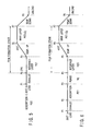
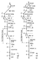
- FIG. 7 is a time chart showing an MOCVD method of a tantalum oxide film according to a fifth embodiment of the present invention.
- the fifth embodiment is characterized in that a formation stage of a tantalum oxide film is followed by a reformation step and a crystallization step sequentially performed in the same process container 20.
- steps from a time point P1 to a time point P7 are the same as those of the first embodiment shown in FIG. 2. However, in place of the first embodiment, it is possible to use the steps from the time point P1 to the time point P7 of the second embodiment shown in FIG. 4, the third embodiment shown in FIG. 5, or the fourth embodiment shown in FIG. 6.
- the temperature of the wafers W in this step is set to be in a range of from 300 to 600°C, preferably of from 400 to 450°C, and, for example, at the same temperature as the main layer formation step, e.g., about 410°C.
- the reformation process is performed for, e.g., about 3 minutes, so that C-C bonds or hydrocarbons contained in the tantalum oxide film are cut off and dissociated by ozone or oxygen radicals, and defects in the film are repaired.
- the temperature of the wafers W is set to be in a range of from 500 to 750°C, preferably of from 675 to 750°C, and, for example, at about 700°C.
- an inactive gas such as N 2 gas or Ar gas, is supplied into the process container 20, with its flow rate being controlled.
- the crystallization step is performed for a predetermined period of time, e.g., about 3 minutes, to turn the tantalum oxide film from an amorphous state into a crystalline state.
- the temperature of the wafers W is lowered to a predetermined handling temperature of, e.g., about 200°C, with N 2 gas being supplied (a time point P14). Then, the pressure in the process container 20 is returned to the atmospheric pressure, and the wafer boat 44 along with the wafers W is unloaded from the process container 20.
- a predetermined handling temperature e.g., about 200°C
- the formation stage of the tantalum oxide film is followed by the reformation step and the crystallization step sequentially performed in the same process container 20.
- the reformation step and the crystallization step sequentially performed in the same process container 20.
- FIG. 8 is a time chart showing an MOCVD method of a tantalum oxide film according to a sixth embodiment of the present invention.
- the sixth embodiment differs from the fifth embodiment in that a reformation step for a tantalum oxide film is performed again after a crystallization step.
- the temperature of the wafers W is lowered not to a handling temperature, but to a reformation temperature higher than the handling temperature (a time point P15).
- the second reformation step is performed for a predetermined period of time, e.g., about 3 minutes, with the reformation temperature being maintained.
- the process temperature in the second reformation step is set to be in a range of from 300 to 500°C, preferably of from 400 to 450°C, and, for example, at about 410°C.
- the supply of ozone is stopped. Then, the temperature of the wafers W is lowered to a predetermined handling temperature of, e.g., about 200°C, with N 2 gas being supplied (a time point P17). Then, the pressure in the process container 20 is returned to the atmospheric pressure, and the wafer boat 44 along with the wafers W is unloaded from the process container 20.
- a predetermined handling temperature e.g., about 200°C
- the crystallization step of the tantalum oxide film is followed by the second reformation step.
- the bonds in the tantalum oxide film, to which impurities were coupled, but have been dissociated in the crystallization step are coupled with oxygen, thereby improving the electric properties of the tantalum oxide film.
- FIG. 14 is a time chart showing an MOCVD method of a tantalum oxide film according to a seventh embodiment of the present invention.
- the seventh embodiment differs from the fifth and sixth embodiments in that a formation stage of a tantalum oxide film is followed by a reformation step in the same process container 20, without a crystallization step. Specifically, when the formation stage of a tantalum oxide film is finished (the time point P7), an N 2 purge step is conducted, and a reformation step is then performed.
- the process conditions of the reformation step such as a reformation gas, a process temperature, and a process time, are the same as in the fifth embodiment.
- the supply of ozone is stopped. Then, the temperature of the wafers W is lowered to a predetermined handling temperature of, e.g., about 200°C, with N 2 gas being supplied (a time point P11). Then, the pressure in the process container 20 is returned to the atmospheric pressure, and the wafer boat 44 along with the wafers W is unloaded from the process container 20.
- a predetermined handling temperature e.g., about 200°C
- the tantalum oxide film is reformed while the film maintains an amorphous state. As a result, it is possible to form an amorphous tantalum oxide film having excellent electric properties.
- the temperature of the process container 20 is set at 200°C, when the wafers W are loaded and unloaded to and from the process container 20.
- this temperature is not limited to 200°C, but may be set at a temperature of from 200 to 350°C.
- FIGS. 9A to 9C are sectional views showing steps of forming the insulating film of tantalum oxide of a capacitor, which has an MIM structure, by an MOCVD method according to an embodiment of the present invention.
- a lower electrode 3 made of, e.g., ruthenium, for the capacitor is disposed on an inter-level insulating film 5 made of, e.g., SiO 2 .
- the lower electrode 3 is connected to a diffusion layer (not shown) below it through a plug 7 made of, e.g., tungsten.
- a tantalum oxide film 52 is deposited as a capacitor insulating film on the lower electrode 3 and the inter-level insulating film 5.
- a method according to any one of the first to seventh embodiments is used. Specifically, as shown in FIGS.
- the formation stage of a tantalum oxide film is followed by a reformation step and a crystallization step sequentially performed in the same process container, it is possible to improve the throughput of the whole process, and to improve the electric properties of the tantalum oxide film.
- the capacitor shown in FIG. 9C has an MIM structure, the present invention is applicable to the insulating film of a capacitor having an MIS structure.
- FIG. 10 is a sectional view showing a transistor, which employs a tantalum oxide film as the gate insulating film.
- the present invention is applicable to the case of forming this gate insulating film.
- a source 2 and a drain 4 are formed in the surface of a semiconductor wafer W made of, e.g., silicon.
- a semiconductor wafer W made of, e.g., silicon.
- an underlying layer 6 On the surface between the source and drain 2 and 4, an underlying layer 6, a tantalum oxide film 52 functioning as the gate insulating film, a barrier metal layer 10, and a gate electrode 12 are stacked in this order.
- the underlying layer 6 consists essentially of any one of silicon oxide (SiOx), silicon nitride (SiNx), and a mixture of them (SiOxNy).
- the barrier metal layer 10 is made of, e.g., TiN, to prevent the tantalum oxide film 52 and the gate electrode 12 from reacting with each other.
- the gate electrode 12 is made of Al (aluminum) or W (tungsten).
- an interface layer 50 is first deposited by an interface layer formation step, and a main layer 51 is then deposited thereon by a main layer formation step, thereby forming the tantalum oxide film 52.
- the tantalum oxide film 52 is formed to have a uniform thickness, because there is no incubation time, i.e., no time lag in film formation.
- the present invention may be applied to an MOCVD apparatus of the batch type with a process container having a double-tube structure.
- the present invention may be applied to an MOCVD apparatus of the single-substrate-processing type.
- the present invention may be applied to a target substrate other than a semiconductor wafer, such as an LCD substrate, or a glass substrate.
Landscapes
- Chemical & Material Sciences (AREA)
- General Chemical & Material Sciences (AREA)
- Chemical Kinetics & Catalysis (AREA)
- Engineering & Computer Science (AREA)
- Materials Engineering (AREA)
- Mechanical Engineering (AREA)
- Metallurgy (AREA)
- Organic Chemistry (AREA)
- Inorganic Chemistry (AREA)
- Chemical Vapour Deposition (AREA)
- Formation Of Insulating Films (AREA)
- Semiconductor Memories (AREA)
Applications Claiming Priority (4)
| Application Number | Priority Date | Filing Date | Title |
|---|---|---|---|
| JP2000080904 | 2000-03-22 | ||
| JP2000080904 | 2000-03-22 | ||
| JP2000370667A JP3437832B2 (ja) | 2000-03-22 | 2000-12-05 | 成膜方法及び成膜装置 |
| JP2000370667 | 2000-12-05 |
Publications (2)
| Publication Number | Publication Date |
|---|---|
| EP1136588A2 true EP1136588A2 (fr) | 2001-09-26 |
| EP1136588A3 EP1136588A3 (fr) | 2003-11-26 |
Family
ID=26588103
Family Applications (1)
| Application Number | Title | Priority Date | Filing Date |
|---|---|---|---|
| EP01106421A Withdrawn EP1136588A3 (fr) | 2000-03-22 | 2001-03-21 | Méthode MOCVD d'un film d'oxyde de tantale |
Country Status (5)
| Country | Link |
|---|---|
| US (1) | US6313047B2 (fr) |
| EP (1) | EP1136588A3 (fr) |
| JP (1) | JP3437832B2 (fr) |
| KR (1) | KR100737056B1 (fr) |
| TW (1) | TW504773B (fr) |
Families Citing this family (44)
| Publication number | Priority date | Publication date | Assignee | Title |
|---|---|---|---|---|
| US6585823B1 (en) * | 2000-07-07 | 2003-07-01 | Asm International, N.V. | Atomic layer deposition |
| JP3437830B2 (ja) | 2000-11-28 | 2003-08-18 | 東京エレクトロン株式会社 | 成膜方法 |
| KR100385952B1 (ko) * | 2001-01-19 | 2003-06-02 | 삼성전자주식회사 | 탄탈륨 산화막을 가진 반도체 커패시터 및 그의 제조방법 |
| KR100425463B1 (ko) * | 2001-09-10 | 2004-03-30 | 삼성전자주식회사 | 산소를 함유하는 활성화된 기체 분위기에서의 탄탈륨산화막 형성 방법 및 유전막 형성 방법 |
| JP4029595B2 (ja) * | 2001-10-15 | 2008-01-09 | 株式会社デンソー | SiC半導体装置の製造方法 |
| KR100444303B1 (ko) * | 2001-12-31 | 2004-08-16 | 주식회사 하이닉스반도체 | 반도체소자의 캐패시터 형성방법 |
| TWI225668B (en) | 2002-05-13 | 2004-12-21 | Tokyo Electron Ltd | Substrate processing method |
| JP4256340B2 (ja) * | 2002-05-16 | 2009-04-22 | 東京エレクトロン株式会社 | 基板処理方法 |
| KR100475077B1 (ko) * | 2002-05-31 | 2005-03-10 | 삼성전자주식회사 | 캐패시터의 유전막 형성방법 |
| JP2004039821A (ja) | 2002-07-02 | 2004-02-05 | Elpida Memory Inc | 半導体装置の製造方法 |
| US20050136657A1 (en) * | 2002-07-12 | 2005-06-23 | Tokyo Electron Limited | Film-formation method for semiconductor process |
| KR20040032198A (ko) * | 2002-10-01 | 2004-04-17 | 주성엔지니어링(주) | 오존을 이용한 탄탈 산화막의 금속유기화학증착 방법 |
| JP4221526B2 (ja) * | 2003-03-26 | 2009-02-12 | キヤノンアネルバ株式会社 | 金属酸化物を基板表面上に形成する成膜方法 |
| US6818517B1 (en) | 2003-08-29 | 2004-11-16 | Asm International N.V. | Methods of depositing two or more layers on a substrate in situ |
| JP4770145B2 (ja) * | 2003-10-07 | 2011-09-14 | 東京エレクトロン株式会社 | 成膜方法及び成膜装置 |
| JP4476880B2 (ja) | 2005-06-24 | 2010-06-09 | 株式会社東芝 | 絶縁膜の形成方法、半導体装置の製造方法、半導体装置 |
| JP5665289B2 (ja) * | 2008-10-29 | 2015-02-04 | 株式会社日立国際電気 | 半導体装置の製造方法、基板処理方法および基板処理装置 |
| JP5307072B2 (ja) * | 2009-06-17 | 2013-10-02 | 東京エレクトロン株式会社 | 金属酸化物膜の形成方法及び成膜装置 |
| JP5270476B2 (ja) | 2009-07-07 | 2013-08-21 | 株式会社日立国際電気 | 半導体装置の製造方法及び基板処理装置 |
| JP5813303B2 (ja) | 2009-11-20 | 2015-11-17 | 株式会社日立国際電気 | 半導体装置の製造方法、基板処理方法および基板処理装置 |
| JP5770892B2 (ja) * | 2009-11-20 | 2015-08-26 | 株式会社日立国際電気 | 半導体装置の製造方法、基板処理方法および基板処理装置 |
| US9611544B2 (en) | 2010-04-15 | 2017-04-04 | Novellus Systems, Inc. | Plasma activated conformal dielectric film deposition |
| US8637411B2 (en) | 2010-04-15 | 2014-01-28 | Novellus Systems, Inc. | Plasma activated conformal dielectric film deposition |
| US9892917B2 (en) | 2010-04-15 | 2018-02-13 | Lam Research Corporation | Plasma assisted atomic layer deposition of multi-layer films for patterning applications |
| US9257274B2 (en) | 2010-04-15 | 2016-02-09 | Lam Research Corporation | Gapfill of variable aspect ratio features with a composite PEALD and PECVD method |
| US9373500B2 (en) | 2014-02-21 | 2016-06-21 | Lam Research Corporation | Plasma assisted atomic layer deposition titanium oxide for conformal encapsulation and gapfill applications |
| US9997357B2 (en) | 2010-04-15 | 2018-06-12 | Lam Research Corporation | Capped ALD films for doping fin-shaped channel regions of 3-D IC transistors |
| US9685320B2 (en) | 2010-09-23 | 2017-06-20 | Lam Research Corporation | Methods for depositing silicon oxide |
| SG10201607194PA (en) * | 2011-09-23 | 2016-10-28 | Novellus Systems Inc | Plasma activated conformal dielectric film deposition |
| JP5780981B2 (ja) * | 2012-03-02 | 2015-09-16 | 東京エレクトロン株式会社 | ゲルマニウム薄膜の成膜方法 |
| SG2013083654A (en) | 2012-11-08 | 2014-06-27 | Novellus Systems Inc | Methods for depositing films on sensitive substrates |
| JP6230809B2 (ja) * | 2013-04-22 | 2017-11-15 | 株式会社日立国際電気 | 半導体装置の製造方法、基板処理装置およびプログラム |
| JP6111171B2 (ja) * | 2013-09-02 | 2017-04-05 | 東京エレクトロン株式会社 | 成膜方法及び成膜装置 |
| US9564312B2 (en) | 2014-11-24 | 2017-02-07 | Lam Research Corporation | Selective inhibition in atomic layer deposition of silicon-containing films |
| US10566187B2 (en) | 2015-03-20 | 2020-02-18 | Lam Research Corporation | Ultrathin atomic layer deposition film accuracy thickness control |
| US9773643B1 (en) | 2016-06-30 | 2017-09-26 | Lam Research Corporation | Apparatus and method for deposition and etch in gap fill |
| US10062563B2 (en) | 2016-07-01 | 2018-08-28 | Lam Research Corporation | Selective atomic layer deposition with post-dose treatment |
| US10037884B2 (en) | 2016-08-31 | 2018-07-31 | Lam Research Corporation | Selective atomic layer deposition for gapfill using sacrificial underlayer |
| JP6456893B2 (ja) | 2016-09-26 | 2019-01-23 | 株式会社Kokusai Electric | 半導体装置の製造方法、記録媒体および基板処理装置 |
| US10269559B2 (en) | 2017-09-13 | 2019-04-23 | Lam Research Corporation | Dielectric gapfill of high aspect ratio features utilizing a sacrificial etch cap layer |
| JP6586443B2 (ja) * | 2017-10-10 | 2019-10-02 | 東京エレクトロン株式会社 | 被処理体を処理する方法 |
| SG11202111962QA (en) | 2019-05-01 | 2021-11-29 | Lam Res Corp | Modulated atomic layer deposition |
| JP2022534793A (ja) | 2019-06-07 | 2022-08-03 | ラム リサーチ コーポレーション | 原子層堆積時における膜特性の原位置制御 |
| CN116282161B (zh) * | 2023-03-14 | 2024-04-30 | 西华师范大学 | 一种基于mocvd的五氧化二钽气凝胶制备方法 |
Family Cites Families (10)
| Publication number | Priority date | Publication date | Assignee | Title |
|---|---|---|---|---|
| JPS62113430A (ja) | 1985-11-12 | 1987-05-25 | Nec Corp | 金属酸化膜の気相成長方法 |
| US5663088A (en) * | 1995-05-19 | 1997-09-02 | Micron Technology, Inc. | Method of forming a Ta2 O5 dielectric layer with amorphous diffusion barrier layer and method of forming a capacitor having a Ta2 O5 dielectric layer and amorphous diffusion barrier layer |
| US6218300B1 (en) * | 1998-06-12 | 2001-04-17 | Applied Materials, Inc. | Method and apparatus for forming a titanium doped tantalum pentaoxide dielectric layer using CVD |
| US6232248B1 (en) * | 1998-07-03 | 2001-05-15 | Tokyo Electron Limited | Single-substrate-heat-processing method for performing reformation and crystallization |
| JP3209965B2 (ja) * | 1998-07-03 | 2001-09-17 | 東京エレクトロン株式会社 | 金属酸化膜の形成方法 |
| US6204203B1 (en) * | 1998-10-14 | 2001-03-20 | Applied Materials, Inc. | Post deposition treatment of dielectric films for interface control |
| US6204204B1 (en) * | 1999-04-01 | 2001-03-20 | Cvc Products, Inc. | Method and apparatus for depositing tantalum-based thin films with organmetallic precursor |
| JP4505098B2 (ja) | 2000-03-08 | 2010-07-14 | 株式会社アルバック | 絶縁膜の成膜方法及びその成膜装置 |
| JP4493796B2 (ja) | 2000-03-30 | 2010-06-30 | 東京エレクトロン株式会社 | 誘電体膜の形成方法 |
| SG90269A1 (en) | 2000-11-13 | 2002-07-23 | Applied Materials Inc | Atomic layer deposition of ta2o5 and high-k dielectrics |
-
2000
- 2000-12-05 JP JP2000370667A patent/JP3437832B2/ja not_active Expired - Fee Related
-
2001
- 2001-03-20 US US09/811,451 patent/US6313047B2/en not_active Expired - Fee Related
- 2001-03-20 TW TW090106513A patent/TW504773B/zh not_active IP Right Cessation
- 2001-03-21 EP EP01106421A patent/EP1136588A3/fr not_active Withdrawn
- 2001-03-22 KR KR1020010014898A patent/KR100737056B1/ko not_active Expired - Fee Related
Non-Patent Citations (5)
| Title |
|---|
| CHANELIERE C ET AL: "Tantalum pentoxide (Ta2O5) thin films for advanced dielectric applications" MATERIALS SCIENCE AND ENGINEERING R: REPORTS, ELSEVIER SEQUOIA S.A., LAUSANNE, CH, vol. 22, no. 6, 25 May 1998 (1998-05-25), pages 269-322, XP004130212 ISSN: 0927-796X * |
| HITCHENS W R ET AL: "TANTALUM OXIDE THIM FILMS FOR DIELECTRIC APPLICATIONS BY LOW-PRESSURE CHEMICAL VAPOR DEPOSITION" JOURNAL OF THE ELECTROCHEMICAL SOCIETY, ELECTROCHEMICAL SOCIETY. MANCHESTER, NEW HAMPSHIRE, US, vol. 140, no. 9, 1 September 1993 (1993-09-01), pages 2615-2621, XP000424115 ISSN: 0013-4651 * |
| KUKLI K ET AL: "Atomic layer epitaxy growth of tantalum oxide thin films from Ta(OC/sub 2/H/sub 5/)/sub 5/ and H/sub 2/O" JOURNAL OF THE ELECTROCHEMICAL SOCIETY, MAY 1995, USA, vol. 142, no. 5, pages 1670-1675, XP002255713 ISSN: 0013-4651 * |
| SHINRIKI H ET AL: "Ethanol-addition-enhanced, chemical vapor deposited tantalum oxide films from Ta(OC/sub 2/H/sub 5/)/sub 5/ and oxygen precursors" JOURNAL OF THE ELECTROCHEMICAL SOCIETY, SEPT. 1998, ELECTROCHEM. SOC, USA, vol. 145, no. 9, pages 3247-3252, XP002255714 ISSN: 0013-4651 * |
| SONG H-J ET AL: "ATOMIC LAYER DEPOSITION OF TA2O5 FILMS USING TA(OC2H5)5 AND NH3" ULTRATHIN SIO2 AND HIGH-K MATERIALS FOR ULSI GATE DIELECTRICS. SAN FRANCISCO, CA, APRIL 5 - 8, 1999, MATERIALS RESEARCH SOCIETY SYMPOSIUM PROCEEDINGS. VOL. 567, WARRENDALE, PA: MRS, US, vol. 567, 5 April 1999 (1999-04-05), pages 469-471, XP000897863 ISBN: 0-55899-474-2 * |
Also Published As
| Publication number | Publication date |
|---|---|
| JP3437832B2 (ja) | 2003-08-18 |
| TW504773B (en) | 2002-10-01 |
| KR20010092714A (ko) | 2001-10-26 |
| JP2001338922A (ja) | 2001-12-07 |
| US20010027031A1 (en) | 2001-10-04 |
| US6313047B2 (en) | 2001-11-06 |
| EP1136588A3 (fr) | 2003-11-26 |
| KR100737056B1 (ko) | 2007-07-09 |
Similar Documents
| Publication | Publication Date | Title |
|---|---|---|
| US6313047B2 (en) | MOCVD method of tantalum oxide film | |
| US7220461B2 (en) | Method and apparatus for forming silicon oxide film | |
| US8435905B2 (en) | Manufacturing method of semiconductor device, and substrate processing apparatus | |
| KR100975268B1 (ko) | 반도체 장치의 제조 방법 및 기판 처리 장치 | |
| US8461059B2 (en) | Batch CVD method and apparatus for semiconductor process | |
| US7462376B2 (en) | CVD method for forming silicon nitride film | |
| EP1042528B1 (fr) | Procede de depot de couches ferroelectriques minces | |
| KR100414156B1 (ko) | 집적회로소자의 캐패시터 제조방법 | |
| JP3437830B2 (ja) | 成膜方法 | |
| JP2001152339A (ja) | 原子層蒸着法を用いた薄膜形成方法 | |
| JP3914362B2 (ja) | タンタル酸化膜を備えたキャパシタ製造方法 | |
| JP2012049506A (ja) | 成膜方法及び成膜装置 | |
| JPWO2007102333A1 (ja) | ルテニウム膜の成膜方法およびコンピュータ読取可能な記憶媒体 | |
| US6537876B2 (en) | Method of manufacturing a semiconductor capacitor having a hemispherical grain layer using a dry cleaning process | |
| US7041546B2 (en) | Film forming method for depositing a plurality of high-k dielectric films | |
| US20070287248A1 (en) | Method for manufacturing capacity element, method for manufacturing semiconductor device and semiconductor-manufacturing apparatus | |
| JP2004158811A (ja) | 半導体装置の製造方法 | |
| US7524766B2 (en) | Method for manufacturing semiconductor device and substrate processing apparatus | |
| US8586430B2 (en) | Method of forming dielectric film and capacitor manufacturing method using the same | |
| KR20040008527A (ko) | 반도체 소자의 제조방법 | |
| KR20010004751A (ko) | 반도체 소자의 캐패시터 제조 방법 | |
| US7229917B2 (en) | Film formation method and apparatus for semiconductor process | |
| KR20050056408A (ko) | 반도체 소자의 캐패시터 제조방법 | |
| JPH06163519A (ja) | 酸化タンタル薄膜の製造方法 | |
| KR100382370B1 (ko) | 어닐링장치의 서셉터 전처리방법 |
Legal Events
| Date | Code | Title | Description |
|---|---|---|---|
| PUAI | Public reference made under article 153(3) epc to a published international application that has entered the european phase |
Free format text: ORIGINAL CODE: 0009012 |
|
| 17P | Request for examination filed |
Effective date: 20010321 |
|
| AK | Designated contracting states |
Kind code of ref document: A2 Designated state(s): AT BE CH CY DE DK ES FI FR GB GR IE IT LI LU MC NL PT SE TR |
|
| AX | Request for extension of the european patent |
Free format text: AL;LT;LV;MK;RO;SI |
|
| PUAL | Search report despatched |
Free format text: ORIGINAL CODE: 0009013 |
|
| AK | Designated contracting states |
Kind code of ref document: A3 Designated state(s): AT BE CH CY DE DK ES FI FR GB GR IE IT LI LU MC NL PT SE TR |
|
| AX | Request for extension of the european patent |
Extension state: AL LT LV MK RO SI |
|
| RIC1 | Information provided on ipc code assigned before grant |
Ipc: 7C 23C 16/56 B Ipc: 7C 23C 16/40 A |
|
| AKX | Designation fees paid |
Designated state(s): DE FR GB IT NL |
|
| 17Q | First examination report despatched |
Effective date: 20090617 |
|
| STAA | Information on the status of an ep patent application or granted ep patent |
Free format text: STATUS: THE APPLICATION IS DEEMED TO BE WITHDRAWN |
|
| 18D | Application deemed to be withdrawn |
Effective date: 20091028 |