EP1134801A2 - Méthode de fabrication et de test de structures de circuits electroniques dans un substrat semiconducteur - Google Patents
Méthode de fabrication et de test de structures de circuits electroniques dans un substrat semiconducteur Download PDFInfo
- Publication number
- EP1134801A2 EP1134801A2 EP01106707A EP01106707A EP1134801A2 EP 1134801 A2 EP1134801 A2 EP 1134801A2 EP 01106707 A EP01106707 A EP 01106707A EP 01106707 A EP01106707 A EP 01106707A EP 1134801 A2 EP1134801 A2 EP 1134801A2
- Authority
- EP
- European Patent Office
- Prior art keywords
- structures
- areas
- mask
- gate oxide
- semiconductor substrate
- Prior art date
- Legal status (The legal status is an assumption and is not a legal conclusion. Google has not performed a legal analysis and makes no representation as to the accuracy of the status listed.)
- Withdrawn
Links
Images


Classifications
-
- H10P74/00—
-
- H10P74/277—
Definitions
- the invention relates to a method for producing and Checking at least two structures of an electronic Circuit in a semiconductor substrate.
- Such electronic circuits are typically as integrated circuits on a wafer, preferably one Silicon wafer formed.
- the integrated circuits can for example, be formed by DRAM memory cells.
- On Wafers contain a flat arrangement of a large number of such DRAM memory cells, which are in the form of chips are.
- the chip areas of the individual chips form the Usable areas of the wafer.
- the individual usable areas are of Scored frame, so-called Kerfs edged. In this scratch frame there are electronic circuits by means of which the Functionality and reliability of the electronic Circuits on the individual chip areas is checked.
- Chips with standard DRAM memory cells usually have an arrangement of transistors with a certain gate oxide thickness on. To check these transistors are in transistors of identical design are arranged in the scoring frame. This Transistors in the scoring frame form monitoring and reliability structures, the specified measuring and test steps are used. Based on this measurement and Test steps can be statements about the functionality and reliability of the transistors on the chip areas of the derive individual chips.
- the invention is based on the object of a method create which is the most reliable review possible different structures of an electronic circuit in guaranteed a semiconductor substrate without Usable space is restricted.
- the inventive method for manufacturing and checking at least two structures of an electronic circuit in a semiconductor substrate comprises the following process steps:
- the first structures in the scoring frames of the first areas and the structures in the scoring frames of the second areas are used to review the first and second structures, respectively used in the usable areas.
- the basic idea of the invention is therefore that with the two masks in the respective first or second areas identically trained first and second structures are generated, however, in the scratch frame either only first or only second structures are created.
- the first and second areas are alternating and preferably like a chessboard over the entire surface of the Distributed semiconductor substrate.
- the first areas are only the first structures are arranged in the scoring frame, so in these areas just a review of the first Structures take place even though in the assigned usable areas both first and second structures are located.
- Corresponding are only second structures in the second areas arranged so that only their functionality can be checked there is, although in the assigned usable areas of second areas are both first and second structures.
- both scoring frames in both Areas only one structure of electronic circuits at a time is present, so the number of structures in a scoring frame can be kept small.
- the area of the scoring frame is correspondingly small and that Usable areas can be dimensioned accordingly large, so that a correspondingly high yield in the manufacture of electronic circuits obtained on the semiconductor substrate becomes.
- the complementary arrangement of the first and second structures in the scribe frames of the first and second Ensures reliability and areas Functionality of both structures with a sufficient high process reliability can be checked.
- the checkered arrangement is the first and second areas. In this way, the first and second structures in the respective scoring frame evenly distributed over the surface of the semiconductor substrate, so that when checking the first and second structures the surface of the semiconductor substrate each covered evenly becomes.
- the two masks are particularly advantageous for training the first and second structures only during a technology start-up phase used.
- a technology start-up phase for products manufactured with the semiconductor substrates there is an increased need for measurement and test steps to ensure the reliability of the products sufficiently check.
- one modified first mask instead of using two masks Manufacturing the first and second structures one modified first mask can be used.
- This modified first mask has no division into the first and second areas. Rather, the mask is designed that the first and second in all usable areas Structures are created. In the scoring frame are each generates a predetermined number of first and second structures, so that both structures in a scratch frame be checked at the same time.
- the first and second structures of different gate oxide thicknesses formed by transistors, preferably at DRAM memory cells are used.
- a and 2 schematically show two areas 1, 2 two masks are shown, which are used to manufacture electronic Serve circuits in a semiconductor substrate.
- a The first mask consists of an arrangement of first areas 1 according to FIG. 1.
- a second mask consists of a Arrangement of second areas 2 according to Figure 2.
- Each area 1, 2 of a mask and thus the surface of the semiconductor substrate is divided into a grid of usable areas 3, which are surrounded by scoring frames 4.
- scoring frames 4 In the areas of individual usable areas 3 and scoring frames 4 are two different Structures 5, 6 generated by electronic circuits, their arrangement in Figures 1 and 2 schematically is shown.
- the semiconductor substrate is formed by a silicon wafer, which is used to manufacture DRAM memory cells becomes. Such a silicon wafer becomes a large number won from identical chips. Each of these Chips contains and forms arrays of DRAM memory cells preferably a RAMBUS or the like.
- Such chips are particularly different Structures 5, 6 required by electronic circuits as transistors with different gate oxide thicknesses are formed.
- the first structure forming transistors have a thin gate oxide layer and the transistors forming a second structure are thick Have gate oxide layer.
- the different first and second structures 5, 6 are generated with the masks according to Figures 1 and 2.
- a nitrogen implantation is carried out to produce the first structures 5 in the gate oxide areas of each Transistors.
- the nitrogen is replaced by appropriate Openings in the masks according to Figures 1 and 2 in the Semiconductor substrate implanted.
- the masks 1 and 2 designed so that the gate oxide regions of the gate oxide regions forming the second structures 6 are covered during nitrogen implantation.
- the Oxide layers forming gate oxide layers on the semiconductor substrate upset.
- the Oxide layers forming gate oxide layers on the semiconductor substrate upset.
- Gate oxide regions of those which form the first structures 5 Transistors are slowed down by the nitrogen and inhibited growth of the oxide layers, so that thin gate oxide layers be preserved.
- the non-nitrogen implanted gate oxide areas of the second structures 6 forming transistors thick gate oxide layers receive.
- Each area 1, 2 shown in Figures 1 and 2 the first and second mask each have an identical one Building on.
- Each area 1, 2 comprises in the present example three usable areas 3, which are the chip areas to be generated Chips correspond. These usable areas 3 are of one Scored frame 4.
- the width of the scoring frame 4 is considerable smaller than the width of a usable area 3.
- the chip surfaces have an exemplary embodiment rectangular cross-section, with the bordering this Scoring frame 4 also has a rectangular contour.
- the areas 1, 2 shown in Figures 1 and 2 The first and second mask differ in their training of test structures in the scoring frame 4.
- the scoring frame 4 is the first Mask designed such that only first structures 5 there forming transistors arranged with thin gate oxide layers are.
- the first mask consists of an arrangement of first areas 1, which is complementary to the arrangement of the second areas 2 of the second mask are arranged.
- first and second structures 5, 6 are generated.
- second process step are carried out by means of the second Areas 2 of the second mask in the in the first method step unprocessed areas of the wafer in turn first and second structures 5, 6 generated.
- the first and second areas 1, 2 are the first and the second mask are arranged so that they alternate Arrangement cover the surface of the wafer.
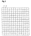
- Figure 3 shows an embodiment of such an arrangement, in which the first areas 1 of the first mask and the second areas 2 of the second mask the wafer surface cover in a checkerboard shape.
- the first and second structures 5, 6 are checked spatially separated in the first and second areas 1, 2 of the two masks that are evenly over the wafer surface are distributed.
- Such an arrangement is particularly advantageous if because in the areas of the scoring frame 4 each one is sufficient generates a large number of first or second structures 5, 6 is used to provide a reliable statistical evaluation of the individual measurement parameters. At the same time, the total number of first or second structures 5, 6 in the areas the scoring frame 4 so small that the total area of the Scoring frame 4 can be kept small.
- the two masks are preferably only sporadic used for some production lots.
- a modified first mask is used instead of the two masks.
- a region 1 'of the modified first mask is shown in Figure 4.
- the first area 1 in turn has usable areas 3 in which again the patterns of the first and second structures 5, 6 are generated.
- These usable areas 3 are identical to the usable areas 3 of the two masks according to FIGS. 1 and 2.
- the mask according to Figure 4 predominantly first in the area of scoring frames 4 Structures 5 forming transistors with thin gate oxide layers generated, whereas only a small number of second Structures 6 is generated.
Landscapes
- Testing Or Measuring Of Semiconductors Or The Like (AREA)
- Preparing Plates And Mask In Photomechanical Process (AREA)
- Tests Of Electronic Circuits (AREA)
Applications Claiming Priority (2)
| Application Number | Priority Date | Filing Date | Title |
|---|---|---|---|
| DE10014914 | 2000-03-17 | ||
| DE10014914A DE10014914C2 (de) | 2000-03-17 | 2000-03-17 | Verfahren zur Herstellung und Überprüfung von Strukturen elektronischer Schaltungen in einem Halbleitersubstrat |
Publications (2)
| Publication Number | Publication Date |
|---|---|
| EP1134801A2 true EP1134801A2 (fr) | 2001-09-19 |
| EP1134801A3 EP1134801A3 (fr) | 2008-05-07 |
Family
ID=7636375
Family Applications (1)
| Application Number | Title | Priority Date | Filing Date |
|---|---|---|---|
| EP01106707A Withdrawn EP1134801A3 (fr) | 2000-03-17 | 2001-03-16 | Méthode de fabrication et de test de structures de circuits electroniques dans un substrat semiconducteur |
Country Status (6)
| Country | Link |
|---|---|
| US (1) | US6484307B2 (fr) |
| EP (1) | EP1134801A3 (fr) |
| JP (1) | JP3732100B2 (fr) |
| KR (1) | KR100441324B1 (fr) |
| DE (1) | DE10014914C2 (fr) |
| TW (1) | TW484225B (fr) |
Families Citing this family (8)
| Publication number | Priority date | Publication date | Assignee | Title |
|---|---|---|---|---|
| US6733728B1 (en) * | 1996-03-11 | 2004-05-11 | Hitachi, Ltd. | Analyzer system having sample rack transfer line |
| US6934200B2 (en) * | 2001-03-12 | 2005-08-23 | Indian Institute Of Science | Yield and speed enhancement of semiconductor integrated circuits using post fabrication transistor mismatch compensation circuitry |
| DE10149885B4 (de) | 2001-10-10 | 2006-03-23 | Infineon Technologies Ag | Testwafer und Verfahren zu dessen Herstellung |
| US6785009B1 (en) * | 2002-02-28 | 2004-08-31 | Advanced Micro Devices, Inc. | Method of using high yielding spectra scatterometry measurements to control semiconductor manufacturing processes, and systems for accomplishing same |
| US7289659B2 (en) * | 2003-06-20 | 2007-10-30 | International Business Machines Corporation | Method and apparatus for manufacturing diamond shaped chips |
| US20050130432A1 (en) * | 2003-12-11 | 2005-06-16 | Machala Charles F.Iii | Method for improving transistor leakage current uniformity |
| US20070156365A1 (en) * | 2006-01-05 | 2007-07-05 | International Business Machines Corporation | Method and system to define multiple metrology criteria for defect screening of electrical connections |
| CN116068844B (zh) * | 2023-03-10 | 2023-07-07 | 合肥晶合集成电路股份有限公司 | 一种掩模板及晶圆的制备方法 |
Family Cites Families (11)
| Publication number | Priority date | Publication date | Assignee | Title |
|---|---|---|---|---|
| US3774088A (en) * | 1972-12-29 | 1973-11-20 | Ibm | An integrated circuit test transistor structure and method of fabricating the same |
| JPS59208848A (ja) * | 1983-05-13 | 1984-11-27 | Hitachi Ltd | 半導体装置の製造法 |
| US5097422A (en) * | 1986-10-10 | 1992-03-17 | Cascade Design Automation Corporation | Method and apparatus for designing integrated circuits |
| JPS6459231A (en) * | 1987-08-31 | 1989-03-06 | Dainippon Printing Co Ltd | Mask layout method for semiconductor integrated circuit |
| US5217916A (en) * | 1989-10-03 | 1993-06-08 | Trw Inc. | Method of making an adaptive configurable gate array |
| US5523252A (en) * | 1993-08-26 | 1996-06-04 | Seiko Instruments Inc. | Method for fabricating and inspecting semiconductor integrated circuit substrate, and semi-finished product used for the sustrate |
| US5682320A (en) * | 1994-06-03 | 1997-10-28 | Synopsys, Inc. | Method for electronic memory management during estimation of average power consumption of an electronic circuit |
| KR100248793B1 (ko) * | 1996-06-25 | 2000-03-15 | 김영환 | 반도체장치 제조시의 패턴 모니터링을 위한 버어니어 |
| US5923047A (en) * | 1997-04-21 | 1999-07-13 | Lsi Logic Corporation | Semiconductor die having sacrificial bond pads for die test |
| DE19717791C2 (de) * | 1997-04-26 | 1999-07-22 | Micronas Semiconductor Holding | Testtransistor und Verfahren zum Herstellen |
| KR19990000215A (ko) * | 1997-06-03 | 1999-01-15 | 문정환 | 포스트 마스크의 검사패턴 |
-
2000
- 2000-03-17 DE DE10014914A patent/DE10014914C2/de not_active Expired - Fee Related
-
2001
- 2001-03-15 JP JP2001074473A patent/JP3732100B2/ja not_active Expired - Fee Related
- 2001-03-16 EP EP01106707A patent/EP1134801A3/fr not_active Withdrawn
- 2001-03-16 KR KR10-2001-0013588A patent/KR100441324B1/ko not_active Expired - Fee Related
- 2001-03-19 US US09/811,867 patent/US6484307B2/en not_active Expired - Lifetime
- 2001-05-14 TW TW090106212A patent/TW484225B/zh not_active IP Right Cessation
Also Published As
| Publication number | Publication date |
|---|---|
| TW484225B (en) | 2002-04-21 |
| KR100441324B1 (ko) | 2004-07-23 |
| US6484307B2 (en) | 2002-11-19 |
| DE10014914A1 (de) | 2001-10-04 |
| DE10014914C2 (de) | 2003-07-24 |
| JP3732100B2 (ja) | 2006-01-05 |
| JP2001313319A (ja) | 2001-11-09 |
| KR20010090459A (ko) | 2001-10-18 |
| EP1134801A3 (fr) | 2008-05-07 |
| US20020016693A1 (en) | 2002-02-07 |
Similar Documents
| Publication | Publication Date | Title |
|---|---|---|
| DE69219165T2 (de) | Prüf- und Einbrennsystem für einen Wafer und Methode für deren Herstellung | |
| DE112018003756B4 (de) | Prüfung und initialisierung von klein-chips auf wafer-niveau | |
| DE1957788A1 (de) | Verfahren zur Erzielung einer optischen Ausbeute bei der Herstellung von integrierten Schaltungen | |
| DE2418906A1 (de) | Verfahren zur verbindung der in einer halbleiterscheibe erzeugten schaltungskreise | |
| DE19835840A1 (de) | Struktur eines Halbleiter-Wafers und Herstellungsverfahren für einen Halbleiterchip | |
| DE10036961B4 (de) | Verfahren zum Testen von Halbleiterwafern unter Verwendung von in Unterbereiche aufgeteilten Bereichen | |
| DE10014914C2 (de) | Verfahren zur Herstellung und Überprüfung von Strukturen elektronischer Schaltungen in einem Halbleitersubstrat | |
| DE3304255C2 (de) | Verfahren zur Herstellung einer Halbleiteranordnung, bei dem eine Getterbehandlung erfolgt | |
| DE3016050C2 (de) | Verfahren zur Herstellung von Fotolackstrukturen für integrierte Halbleiterschaltungsanordnungen | |
| EP0167732B1 (fr) | Procédé pour la fabrication d'un matériau de base pour un circuit hybride | |
| DE102004058411B3 (de) | Halbleiterwafer mit einer Teststruktur und Verfahren | |
| DE69012345T2 (de) | Methode und vorrichtung für fehlanalyse in halbleiterfabrikation. | |
| DE10056872C1 (de) | Implantationsüberwachung unter Anwendung mehrerer Implantations- und Temperschritte | |
| DE19906396C2 (de) | Verfahren und System zum Bestimmen der Fehlerstrukturen von hergestellten Halbleiterscheiben bei einer automatisierten Halbleiterscheiben-Abnahmeprüfung | |
| DE102004060369A1 (de) | Halbleiterscheibe mit Teststruktur | |
| EP1128424A2 (fr) | Structure d'essaiage près de semi-conducteurs intégrés | |
| DE69033386T2 (de) | Elektrisches Verfahren, um Positionsfehler an den Kontaktöffnungen in einer Halbleitervorrichtung zu erkennen | |
| DE19743765A1 (de) | Verfahren zum Herstellen eines Halbleiterbauteils mit einem Muster zur Verhinderung von Rißbildung | |
| DE3530578A1 (de) | Struktur zur qualitaetspruefung einer substratscheibe aus halbleitermaterial | |
| DE2453578A1 (de) | Verfahren zum feststellen von vollstaendig durchgehenden bohrungen in einer auf einem halbleitersubstrat angebrachten isolierschicht | |
| DE3630388A1 (de) | Programmierbare logische anordung | |
| DE19819252A1 (de) | Halbleiterspeichervorrichtung | |
| DE102005002678A1 (de) | Ritzrahmen mit verbesserter Füllroutine | |
| DE10128269A1 (de) | Eine Chipflächen-Justierstruktur | |
| EP1333293B1 (fr) | Procédé pour l'analyse des défaillances durant la fabrication de plaquettes de semi-conducteur |
Legal Events
| Date | Code | Title | Description |
|---|---|---|---|
| PUAI | Public reference made under article 153(3) epc to a published international application that has entered the european phase |
Free format text: ORIGINAL CODE: 0009012 |
|
| AK | Designated contracting states |
Kind code of ref document: A2 Designated state(s): AT BE CH CY DE DK ES FI FR GB GR IE IT LI LU MC NL PT SE TR |
|
| AX | Request for extension of the european patent |
Free format text: AL;LT;LV;MK;RO;SI |
|
| PUAL | Search report despatched |
Free format text: ORIGINAL CODE: 0009013 |
|
| AK | Designated contracting states |
Kind code of ref document: A3 Designated state(s): AT BE CH CY DE DK ES FI FR GB GR IE IT LI LU MC NL PT SE TR |
|
| AX | Request for extension of the european patent |
Extension state: AL LT LV MK RO SI |
|
| 17P | Request for examination filed |
Effective date: 20080527 |
|
| 17Q | First examination report despatched |
Effective date: 20080718 |
|
| AKX | Designation fees paid |
Designated state(s): DE |
|
| RAP1 | Party data changed (applicant data changed or rights of an application transferred) |
Owner name: QIMONDA AG |
|
| 19U | Interruption of proceedings before grant |
Effective date: 20090401 |
|
| 19W | Proceedings resumed before grant after interruption of proceedings |
Effective date: 20091123 |
|
| GRAP | Despatch of communication of intention to grant a patent |
Free format text: ORIGINAL CODE: EPIDOSNIGR1 |
|
| RIC1 | Information provided on ipc code assigned before grant |
Ipc: H01L 23/544 20060101AFI20100204BHEP |
|
| STAA | Information on the status of an ep patent application or granted ep patent |
Free format text: STATUS: THE APPLICATION IS DEEMED TO BE WITHDRAWN |
|
| 18D | Application deemed to be withdrawn |
Effective date: 20100629 |