EP1134801A2 - Method of fabrication and testing of electronic circuit structures in a semiconducting substrate - Google Patents
Method of fabrication and testing of electronic circuit structures in a semiconducting substrate Download PDFInfo
- Publication number
- EP1134801A2 EP1134801A2 EP01106707A EP01106707A EP1134801A2 EP 1134801 A2 EP1134801 A2 EP 1134801A2 EP 01106707 A EP01106707 A EP 01106707A EP 01106707 A EP01106707 A EP 01106707A EP 1134801 A2 EP1134801 A2 EP 1134801A2
- Authority
- EP
- European Patent Office
- Prior art keywords
- structures
- areas
- mask
- gate oxide
- semiconductor substrate
- Prior art date
- Legal status (The legal status is an assumption and is not a legal conclusion. Google has not performed a legal analysis and makes no representation as to the accuracy of the status listed.)
- Withdrawn
Links
Images


Classifications
-
- H—ELECTRICITY
- H01—ELECTRIC ELEMENTS
- H01L—SEMICONDUCTOR DEVICES NOT COVERED BY CLASS H10
- H01L22/00—Testing or measuring during manufacture or treatment; Reliability measurements, i.e. testing of parts without further processing to modify the parts as such; Structural arrangements therefor
-
- H—ELECTRICITY
- H01—ELECTRIC ELEMENTS
- H01L—SEMICONDUCTOR DEVICES NOT COVERED BY CLASS H10
- H01L22/00—Testing or measuring during manufacture or treatment; Reliability measurements, i.e. testing of parts without further processing to modify the parts as such; Structural arrangements therefor
- H01L22/30—Structural arrangements specially adapted for testing or measuring during manufacture or treatment, or specially adapted for reliability measurements
- H01L22/34—Circuits for electrically characterising or monitoring manufacturing processes, e. g. whole test die, wafers filled with test structures, on-board-devices incorporated on each die, process control monitors or pad structures thereof, devices in scribe line
Definitions
- the invention relates to a method for producing and Checking at least two structures of an electronic Circuit in a semiconductor substrate.
- Such electronic circuits are typically as integrated circuits on a wafer, preferably one Silicon wafer formed.
- the integrated circuits can for example, be formed by DRAM memory cells.
- On Wafers contain a flat arrangement of a large number of such DRAM memory cells, which are in the form of chips are.
- the chip areas of the individual chips form the Usable areas of the wafer.
- the individual usable areas are of Scored frame, so-called Kerfs edged. In this scratch frame there are electronic circuits by means of which the Functionality and reliability of the electronic Circuits on the individual chip areas is checked.
- Chips with standard DRAM memory cells usually have an arrangement of transistors with a certain gate oxide thickness on. To check these transistors are in transistors of identical design are arranged in the scoring frame. This Transistors in the scoring frame form monitoring and reliability structures, the specified measuring and test steps are used. Based on this measurement and Test steps can be statements about the functionality and reliability of the transistors on the chip areas of the derive individual chips.
- the invention is based on the object of a method create which is the most reliable review possible different structures of an electronic circuit in guaranteed a semiconductor substrate without Usable space is restricted.
- the inventive method for manufacturing and checking at least two structures of an electronic circuit in a semiconductor substrate comprises the following process steps:
- the first structures in the scoring frames of the first areas and the structures in the scoring frames of the second areas are used to review the first and second structures, respectively used in the usable areas.
- the basic idea of the invention is therefore that with the two masks in the respective first or second areas identically trained first and second structures are generated, however, in the scratch frame either only first or only second structures are created.
- the first and second areas are alternating and preferably like a chessboard over the entire surface of the Distributed semiconductor substrate.
- the first areas are only the first structures are arranged in the scoring frame, so in these areas just a review of the first Structures take place even though in the assigned usable areas both first and second structures are located.
- Corresponding are only second structures in the second areas arranged so that only their functionality can be checked there is, although in the assigned usable areas of second areas are both first and second structures.
- both scoring frames in both Areas only one structure of electronic circuits at a time is present, so the number of structures in a scoring frame can be kept small.
- the area of the scoring frame is correspondingly small and that Usable areas can be dimensioned accordingly large, so that a correspondingly high yield in the manufacture of electronic circuits obtained on the semiconductor substrate becomes.
- the complementary arrangement of the first and second structures in the scribe frames of the first and second Ensures reliability and areas Functionality of both structures with a sufficient high process reliability can be checked.
- the checkered arrangement is the first and second areas. In this way, the first and second structures in the respective scoring frame evenly distributed over the surface of the semiconductor substrate, so that when checking the first and second structures the surface of the semiconductor substrate each covered evenly becomes.
- the two masks are particularly advantageous for training the first and second structures only during a technology start-up phase used.
- a technology start-up phase for products manufactured with the semiconductor substrates there is an increased need for measurement and test steps to ensure the reliability of the products sufficiently check.
- one modified first mask instead of using two masks Manufacturing the first and second structures one modified first mask can be used.
- This modified first mask has no division into the first and second areas. Rather, the mask is designed that the first and second in all usable areas Structures are created. In the scoring frame are each generates a predetermined number of first and second structures, so that both structures in a scratch frame be checked at the same time.
- the first and second structures of different gate oxide thicknesses formed by transistors, preferably at DRAM memory cells are used.
- a and 2 schematically show two areas 1, 2 two masks are shown, which are used to manufacture electronic Serve circuits in a semiconductor substrate.
- a The first mask consists of an arrangement of first areas 1 according to FIG. 1.
- a second mask consists of a Arrangement of second areas 2 according to Figure 2.
- Each area 1, 2 of a mask and thus the surface of the semiconductor substrate is divided into a grid of usable areas 3, which are surrounded by scoring frames 4.
- scoring frames 4 In the areas of individual usable areas 3 and scoring frames 4 are two different Structures 5, 6 generated by electronic circuits, their arrangement in Figures 1 and 2 schematically is shown.
- the semiconductor substrate is formed by a silicon wafer, which is used to manufacture DRAM memory cells becomes. Such a silicon wafer becomes a large number won from identical chips. Each of these Chips contains and forms arrays of DRAM memory cells preferably a RAMBUS or the like.
- Such chips are particularly different Structures 5, 6 required by electronic circuits as transistors with different gate oxide thicknesses are formed.
- the first structure forming transistors have a thin gate oxide layer and the transistors forming a second structure are thick Have gate oxide layer.
- the different first and second structures 5, 6 are generated with the masks according to Figures 1 and 2.
- a nitrogen implantation is carried out to produce the first structures 5 in the gate oxide areas of each Transistors.
- the nitrogen is replaced by appropriate Openings in the masks according to Figures 1 and 2 in the Semiconductor substrate implanted.
- the masks 1 and 2 designed so that the gate oxide regions of the gate oxide regions forming the second structures 6 are covered during nitrogen implantation.
- the Oxide layers forming gate oxide layers on the semiconductor substrate upset.
- the Oxide layers forming gate oxide layers on the semiconductor substrate upset.
- Gate oxide regions of those which form the first structures 5 Transistors are slowed down by the nitrogen and inhibited growth of the oxide layers, so that thin gate oxide layers be preserved.
- the non-nitrogen implanted gate oxide areas of the second structures 6 forming transistors thick gate oxide layers receive.
- Each area 1, 2 shown in Figures 1 and 2 the first and second mask each have an identical one Building on.
- Each area 1, 2 comprises in the present example three usable areas 3, which are the chip areas to be generated Chips correspond. These usable areas 3 are of one Scored frame 4.
- the width of the scoring frame 4 is considerable smaller than the width of a usable area 3.
- the chip surfaces have an exemplary embodiment rectangular cross-section, with the bordering this Scoring frame 4 also has a rectangular contour.
- the areas 1, 2 shown in Figures 1 and 2 The first and second mask differ in their training of test structures in the scoring frame 4.
- the scoring frame 4 is the first Mask designed such that only first structures 5 there forming transistors arranged with thin gate oxide layers are.
- the first mask consists of an arrangement of first areas 1, which is complementary to the arrangement of the second areas 2 of the second mask are arranged.
- first and second structures 5, 6 are generated.
- second process step are carried out by means of the second Areas 2 of the second mask in the in the first method step unprocessed areas of the wafer in turn first and second structures 5, 6 generated.
- the first and second areas 1, 2 are the first and the second mask are arranged so that they alternate Arrangement cover the surface of the wafer.
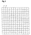
- Figure 3 shows an embodiment of such an arrangement, in which the first areas 1 of the first mask and the second areas 2 of the second mask the wafer surface cover in a checkerboard shape.
- the first and second structures 5, 6 are checked spatially separated in the first and second areas 1, 2 of the two masks that are evenly over the wafer surface are distributed.
- Such an arrangement is particularly advantageous if because in the areas of the scoring frame 4 each one is sufficient generates a large number of first or second structures 5, 6 is used to provide a reliable statistical evaluation of the individual measurement parameters. At the same time, the total number of first or second structures 5, 6 in the areas the scoring frame 4 so small that the total area of the Scoring frame 4 can be kept small.
- the two masks are preferably only sporadic used for some production lots.
- a modified first mask is used instead of the two masks.
- a region 1 'of the modified first mask is shown in Figure 4.
- the first area 1 in turn has usable areas 3 in which again the patterns of the first and second structures 5, 6 are generated.
- These usable areas 3 are identical to the usable areas 3 of the two masks according to FIGS. 1 and 2.
- the mask according to Figure 4 predominantly first in the area of scoring frames 4 Structures 5 forming transistors with thin gate oxide layers generated, whereas only a small number of second Structures 6 is generated.
Landscapes
- Engineering & Computer Science (AREA)
- Manufacturing & Machinery (AREA)
- Computer Hardware Design (AREA)
- Microelectronics & Electronic Packaging (AREA)
- Power Engineering (AREA)
- Automation & Control Theory (AREA)
- Testing Or Measuring Of Semiconductors Or The Like (AREA)
- Preparing Plates And Mask In Photomechanical Process (AREA)
- Tests Of Electronic Circuits (AREA)
Abstract
Die Erfindung betrifft ein Verfahren zur Herstellung und
Überprüfung wenigstens zweier Strukturen (5, 6) einer elektronischen
Schaltung in einem Halbleitersubstrat. Mit zwei unterschiedlichen
Masken werden in zwei Verfahrensschritten in
Nutzflächen (3) des Halbleitersubstrats identische Anordnungen
von ersten und zweiten Strukturen -(5, 6) erzeugt. Im
Ritzrahmen (4), der die Nutzfläche (3) umrandet, werden mit
der ersten Maske nur erste Strukturen (5) und mit der zweiten
Maske nur zweite Strukturen (6) erzeugt.

Description
Die Erfindung betrifft ein Verfahren zur Herstellung und Überprüfung wenigstens zweier Strukturen einer elektronischen Schaltung in einem Halbleitersubstrat.The invention relates to a method for producing and Checking at least two structures of an electronic Circuit in a semiconductor substrate.
Derartige elektronische Schaltungen sind typischerweise als integrierte Schaltungen auf einem Wafer, vorzugsweise einem Silizium-Wafer ausgebildet. Die integrierten Schaltungen können beispielsweise von DRAM-Speicherzellen gebildet sein. Ein Wafer enthält eine flächige Anordnung einer Vielzahl von derartigen DRAM-Speicherzellen, welche in Form von Chips ausgebildet sind. Die Chipflächen der einzelnen Chips bilden die Nutzflächen des Wafers. Die einzelnen Nutzflächen sind von Ritzrahmen, sogenannten Kerfs umrandet. In diesen Ritzrahmen befinden sich elektronische Schaltungen, mittels derer die Funktionsfähigkeit und Zuverlässigkeit der elektronischen Schaltungen auf den einzelnen Chipflächen überprüft wird.Such electronic circuits are typically as integrated circuits on a wafer, preferably one Silicon wafer formed. The integrated circuits can for example, be formed by DRAM memory cells. On Wafers contain a flat arrangement of a large number of such DRAM memory cells, which are in the form of chips are. The chip areas of the individual chips form the Usable areas of the wafer. The individual usable areas are of Scored frame, so-called Kerfs edged. In this scratch frame there are electronic circuits by means of which the Functionality and reliability of the electronic Circuits on the individual chip areas is checked.
Chips mit Standard-DRAM-Speicherzellen weisen üblicherweise eine Anordnung von Transistoren mit einer bestimmten Gate-Oxid-Dicke auf. Zur Überprüfung dieser Transistoren sind in den Ritzrahmen baugleiche Transistoren angeordnet. Diese Transistoren im Ritzrahmen bilden Monitoring- und Zuverlässigkeitsstrukturen, die zur Durchführung vorgegebener Mess- und Prüfschritte verwendet werden. Anhand dieser Mess- und Prüfschritte lassen sich Aussagen über die Funktionsfähigkeit und Zuverlässigkeit der Transistoren auf den Chipflächen der einzelnen Chips ableiten. Chips with standard DRAM memory cells usually have an arrangement of transistors with a certain gate oxide thickness on. To check these transistors are in transistors of identical design are arranged in the scoring frame. This Transistors in the scoring frame form monitoring and reliability structures, the specified measuring and test steps are used. Based on this measurement and Test steps can be statements about the functionality and reliability of the transistors on the chip areas of the derive individual chips.
Um möglichst zuverlässige statistische Aussagen bei den Mess- und Prüfschritten zu erhalten ist es wünschenswert, eine möglichst große Anzahl von Transistoren in den Ritzrahmen zu platzieren. Jedoch ist die maximale Anzahl der Transistoren in den Ritzrahmen dadurch begrenzt, dass die Chip-Ausbeute pro Wafer möglichst hoch sein soll. Dies begrenzt die zur Verfügung stehende Fläche der Ritzrahmen und damit die Anzahl der dort platzierten Transistoren.In order to make the most reliable statistical statements possible and to get test steps it is desirable to get one if possible large number of transistors in the scribe frame too place. However, the maximum number of transistors in the scoring frame limited by the chip yield per wafer should be as high as possible. This limits the Available area of the scoring frame and thus the number of the transistors placed there.
Bei neuartigen DRAM-Speicherzellen, die zum Beispiel für RAMBUS Chips benötigt werden, werden aufgrund der zu erzielenden Leistungsfähigkeit und Zuverlässigkeit derartiger Elemente Transistoren mit mehreren, vorzugsweise zwei unterschiedlichen Gate-Oxid-Dicken benötigt.With new DRAM memory cells, for example for RAMBUS chips are needed due to the achievable Performance and reliability of such elements Transistors with several, preferably two different ones Gate oxide thicknesses required.
Dementsprechend müssen zur Überprüfung dieser Strukturen in den Ritzrahmen Transistoren sowohl mit geringen als auch mit großen Gate-Oxid-Dicken vorgesehen werden, damit die Funktionsfähigkeit und Zuverlässigkeit beider Strukturen abprüfbar ist.Accordingly, to review these structures in the scribing transistors with both low and Large gate oxide thicknesses are provided to ensure functionality and reliability of both structures can be checked is.
Damit im Vergleich zu Standard-DRAM-Speicherzellen für jede Sorte von Transistoren dieselbe Anzahl in den Ritzrahmen zur Verfügung steht, müssten die Flächen der Ritzrahmen vergrößert werden, was zu einer unerwünschten Reduzierung der Chipflächen führen würde.So compared to standard DRAM memory cells for everyone Kind of transistors the same number in the scoring frames Is available, the areas of the scoring frames would have to be enlarged become, resulting in an undesirable reduction in chip area would lead.
Der Erfindung liegt die Aufgabe zugrunde ein Verfahren zu schaffen, welches eine möglichst zuverlässige Überprüfung verschiedener Strukturen einer elektronischen Schaltung in einem Halbleitersubstrat gewährleistet, ohne dass dessen Nutzfläche eingeschränkt wird. The invention is based on the object of a method create which is the most reliable review possible different structures of an electronic circuit in guaranteed a semiconductor substrate without Usable space is restricted.
Zur Lösung dieser Aufgabe sind die Merkmale des Anspruchs 1
vorgesehen. Vorteilhafte Ausführungsformen und zweckmäßige
Weiterbildungen der Erfindung sind in den Unteransprüchen beschrieben.To achieve this object, the features of
Das erfindungsgemäße Verfahren zur Herstellung und Überprüfung wenigstens zweier Strukturen einer elektronischen Schaltung in einem Halbleitersubstrat umfasst folgende Verfahrensschritte:The inventive method for manufacturing and checking at least two structures of an electronic circuit in a semiconductor substrate comprises the following process steps:
Mit einer ersten Maske, bestehend aus einer sich über erste Bereiche des Halbleitersubstrats erstreckenden Anordnung von Nutzflächen und diese umrandenden Ritzrahmen, werden nach einem vorgegebenen Muster erste und zweite Strukturen in den Nutzflächen erzeugt und in den Ritzrahmen erste Strukturen erzeugt.With a first mask consisting of one over first Regions of the semiconductor substrate extending arrangement of Usable areas and these scoring frames, after a given patterns first and second structures in the Usable areas are created and the first structures in the scoring frame generated.
Mit einer zweiten Maske bestehend aus einer sich über zweite Bereiche des Halbleitersubstrats erstreckenden Anordnung von Nutzflächen und diese umrandenden Ritzrahmen werden nach dem vorgegebenen Muster erste und zweite Strukturen in den Nutzflächen erzeugt und in den Ritzrahmen zweite Strukturen erzeugt.With a second mask consisting of one over second Regions of the semiconductor substrate extending arrangement of Usable areas and these scoring frames are after the predetermined pattern first and second structures in the usable areas generated and created second structures in the scratch frame.
Die ersten Strukturen in den Ritzrahmen der ersten Bereiche und die Strukturen in den Ritzrahmen der zweiten Bereiche werden jeweils zur Überprüfung der ersten und zweiten Strukturen in den Nutzflächen verwendet.The first structures in the scoring frames of the first areas and the structures in the scoring frames of the second areas are used to review the first and second structures, respectively used in the usable areas.
Der Grundgedanke der Erfindung liegt somit darin, dass mit den beiden Masken in den jeweiligen ersten oder zweiten Bereichen in den Nutzflächen identisch ausgebildete erste und zweite Strukturen erzeugt werden, jedoch in den Ritzrahmen entweder nur erste oder nur zweite Strukturen erzeugt werden.The basic idea of the invention is therefore that with the two masks in the respective first or second areas identically trained first and second structures are generated, however, in the scratch frame either only first or only second structures are created.
Die ersten und zweiten Bereiche sind dabei alternierend und vorzugsweise schachbrettartig über die gesamte Oberfläche des Halbleitersubstrats verteilt. In den ersten Bereichen sind dabei in den Ritzrahmen nur die ersten Strukturen angeordnet, so dass in diesen Bereichen nur eine Überprüfung von ersten Strukturen erfolgt, obwohl sich in den zugeordneten Nutzflächen sowohl erste als auch zweite Strukturen befinden. Entsprechend sind in den zweiten Bereichen nur zweite Strukturen angeordnet, so dass dort nur deren Funktionsfähigkeit überprüfbar ist, obwohl sich in den zugeordneten Nutzflächen der zweiten Bereiche sowohl erste und zweite Strukturen befinden.The first and second areas are alternating and preferably like a chessboard over the entire surface of the Distributed semiconductor substrate. In the first areas are only the first structures are arranged in the scoring frame, so in these areas just a review of the first Structures take place even though in the assigned usable areas both first and second structures are located. Corresponding are only second structures in the second areas arranged so that only their functionality can be checked there is, although in the assigned usable areas of second areas are both first and second structures.
Durch diese Anordnung werden die ersten und zweiten Strukturen in separaten Bereichen getrennt geprüft. Ein wesentlicher Vorteil besteht darin, dass in sämtlichen Ritzrahmen beider Bereiche jeweils nur eine Struktur von elektronischen Schaltungen vorhanden ist, so dass die Anzahl der Strukturen in einem Ritzrahmen klein gehalten werden kann. Dies bedeutet, dass die Fläche der Ritzrahmen entsprechend klein und die Nutzflächen entsprechend groß dimensioniert werden können, so dass eine entsprechend hohe Ausbeute bei der Herstellung von elektronischen Schaltungen auf dem Halbleitersubstrat erhalten wird.With this arrangement, the first and second structures tested separately in separate areas. An essential one The advantage is that both scoring frames in both Areas only one structure of electronic circuits at a time is present, so the number of structures in a scoring frame can be kept small. This means, that the area of the scoring frame is correspondingly small and that Usable areas can be dimensioned accordingly large, so that a correspondingly high yield in the manufacture of electronic circuits obtained on the semiconductor substrate becomes.
Gleichzeitig ist durch die komplementäre Anordnung von ersten und zweiten Strukturen in den Ritzrahmen der ersten und zweiten Bereiche gewährleistet, dass die Zuverlässigkeit und Funktionsfähigkeit beider Strukturen mit einer ausreichend hohen Prozesssicherheit überprüft werden kann. Besonders vorteilhaft hierbei ist die schachbrettartige Anordnung der ersten und zweiten Bereiche. Auf diese Weise sind die ersten und zweiten Strukturen in dem jeweiligen Ritzrahmen gleichmäßig über die Oberfläche des Halbleitersubstrats verteilt, so dass bei der Überprüfung der ersten und zweiten Strukturen die Oberfläche des Halbleitersubstrats jeweils gleichmäßig abgedeckt wird.At the same time, the complementary arrangement of the first and second structures in the scribe frames of the first and second Ensures reliability and areas Functionality of both structures with a sufficient high process reliability can be checked. Particularly advantageous the checkered arrangement is the first and second areas. In this way, the first and second structures in the respective scoring frame evenly distributed over the surface of the semiconductor substrate, so that when checking the first and second structures the surface of the semiconductor substrate each covered evenly becomes.
Besonders vorteilhaft werden die beiden Masken zur Ausbildung der ersten und zweiten Strukturen nur während einer Technologie-Anlaufphase verwendet. Während einer Technologie-Anlaufphase für mit den Halbleitersubstraten hergestellten Produkten besteht für diese ein erhöhter Bedarf an Mess- und Prüfschritten um die Zuverlässigkeit der Produkte ausreichend zu prüfen.The two masks are particularly advantageous for training the first and second structures only during a technology start-up phase used. During a technology start-up phase for products manufactured with the semiconductor substrates there is an increased need for measurement and test steps to ensure the reliability of the products sufficiently check.
In einer auf die Technologie-Anlaufphase folgenden Produktionsphase besteht ein vergleichsweise geringerer Bedarf an Mess- und Prüfschritten.In a production phase following the technology start-up phase there is a comparatively lower need Measuring and testing steps.
In diesem Fall kann anstelle der Verwendung zweier Masken zur Herstellung der ersten und zweiten Strukturen eine einzige modifizierte erste Maske verwendet werden.In this case, instead of using two masks Manufacturing the first and second structures one modified first mask can be used.
Diese modifizierte erste Maske weist keine Einteilung in erste und zweite Bereiche auf. Vielmehr ist die Maske so ausgebildet, dass in sämtlichen Nutzflächen die ersten und zweiten Strukturen erzeugt werden. In den Ritzrahmen werden jeweils eine vorgegebene Anzahl von ersten und zweiten Strukturen erzeugt, so dass dann in einem Ritzrahmen beide Strukturen gleichzeitig geprüft werden.This modified first mask has no division into the first and second areas. Rather, the mask is designed that the first and second in all usable areas Structures are created. In the scoring frame are each generates a predetermined number of first and second structures, so that both structures in a scratch frame be checked at the same time.
In einer vorteilhaften Ausführungsform der Erfindung sind die ersten und zweiten Strukturen von unterschiedlichen Gate-Oxid-Dicken von Transistoren gebildet, die vorzugsweise bei DRAM-Speicherzellen eingesetzt werden.In an advantageous embodiment of the invention, the first and second structures of different gate oxide thicknesses formed by transistors, preferably at DRAM memory cells are used.
Die Erfindung wird im nachstehenden anhand der Zeichnungen erläutert. Es zeigen:
- Figur 1:
- Schematische Darstellung eines ersten Bereichs einer ersten Maske zur Herstellung von Strukturen elektronischer Schaltungen in einem Halbleitersubstrat.
- Figur 2:
- Schematische Darstellung eines zweiten Bereichs einer zweiten Maske zur Herstellung von Strukturen elektronischer Schaltungen.
- Figur 3:
- Schematische Darstellung der Verteilung von ersten
Bereichen der ersten Maske gemäß
Figur 1 und zweiten Bereichen der zweiten Maske gemäßFigur 2 über der Oberfläche des Halbleitersubstrats. - Figur 4:
- Schematische Darstellung eines Bereichs einer modifizierten ersten Maske zur Herstellung von Strukturen elektronischer Schaltungen in einem Halbleitersubstrat.
- Figure 1:
- Schematic representation of a first area of a first mask for producing structures of electronic circuits in a semiconductor substrate.
- Figure 2:
- Schematic representation of a second area of a second mask for producing structures of electronic circuits.
- Figure 3:
- Schematic representation of the distribution of first areas of the first mask according to FIG. 1 and second areas of the second mask according to FIG. 2 over the surface of the semiconductor substrate.
- Figure 4:
- Schematic representation of an area of a modified first mask for producing structures of electronic circuits in a semiconductor substrate.
In den Figuren 1 und 2 sind schematisch zwei Bereiche 1, 2
zweier Masken dargestellt, welche zur Herstellung elektronischer
Schaltungen in einem Halbleitersubstrat dienen. Eine
erste Maske besteht dabei aus einer Anordnung von ersten Bereichen
1 gemäß Figur 1. Eine zweite Maske besteht aus einer
Anordnung von zweiten Bereichen 2 gemäß Figur 2. Jeder Bereich
1, 2 einer Maske und damit die Oberfläche des Halbleitersubstrats
ist in ein Raster von Nutzflächen 3 unterteilt,
welche von Ritzrahmen 4 umrandet sind. In den Gebieten der
einzelnen Nutzflächen 3 und Ritzrahmen 4 werden zwei verschiedene
Strukturen 5, 6 von elektronischen Schaltungen erzeugt,
deren Anordnung in den Figuren 1 und 2 schematisch
dargestellt ist.1 and 2 schematically show two
Das Halbleitersubstrat ist von einem Silizium-Wafer gebildet, welcher zur Herstellung von DRAM-Speicherzellen verwendet wird. Aus einem derartigen Silizium-Wafer wird eine große Anzahl von identisch ausgebildeten Chips gewonnen. Jeder dieser Chips enthält Anordnungen von DRAM-Speicherzellen und bildet vorzugsweise einen RAMBUS oder dergleichen.The semiconductor substrate is formed by a silicon wafer, which is used to manufacture DRAM memory cells becomes. Such a silicon wafer becomes a large number won from identical chips. Each of these Chips contains and forms arrays of DRAM memory cells preferably a RAMBUS or the like.
Bei derartigen Chips werden insbesondere unterschiedliche
Strukturen 5, 6 von elektronischen Schaltungen benötigt, welche
als Transistoren mit unterschiedlichen Gate-Oxid-Dicken
gebildet sind.Such chips are particularly
Im vorliegenden Ausführungsbeispiel sind zwei unterschiedliche Transistoren vorgesehen, wobei die eine erste Struktur bildenden Transistoren eine dünne Gate-Oxid-Schicht aufweisen und die eine zweite Struktur bildenden Transistoren eine dicke Gate-Oxid-Schicht aufweisen.In the present embodiment, two are different Transistors provided, the first structure forming transistors have a thin gate oxide layer and the transistors forming a second structure are thick Have gate oxide layer.
Die unterschiedlichen ersten und zweiten Strukturen 5, 6 werden
mit den Masken gemäß den Figuren 1 und 2 erzeugt.The different first and
Zur Erzeugung der ersten Strukturen 5 erfolgt eine Stickstoff-Implantation
in den Gate-Oxid-Bereichen der jeweiligen
Transistoren. Hierzu wird der Stickstoff durch entsprechende
Öffnungen in den Masken gemäß den Figuren 1 und 2 in das
Halbleitersubstrat implantiert. Demgegenüber sind die Masken
gemäß den Figuren 1 und 2 so ausgebildet, dass die Gate-Oxid-Bereiche
der die zweiten Strukturen 6 bildenden Gate-Oxid-Bereiche
während der Stickstoff-Implantation abgedeckt sind.A nitrogen implantation is carried out to produce the
Im Anschluss an die Stickstoff-Implantation werden die die
Gate-Oxid-Schichten bildenden Oxidschichten auf das Halbleitersubstrat
aufgebracht. Bei den mit Stickstoff implantierten
Gate-Oxid-Bereichen der die ersten Strukturen 5 bildenden
Transistoren erfolgt durch den Stickstoff ein verlangsamtes
und gehemmtes Wachstum der Oxidschichten, so dass dünne Gate-Oxid-Schichten
erhalten werden. Demgegenüber werden für die
nicht mit Stickstoff implantierten Gate-Oxid-Bereiche der die
zweiten Strukturen 6 bildenden Transistoren dicke Gate-Oxid-Schichten
erhalten.Following the nitrogen implantation, the
Oxide layers forming gate oxide layers on the semiconductor substrate
upset. For those implanted with nitrogen
Gate oxide regions of those which form the
Die in den Figuren 1 und 2 dargestellten Bereiche 1, 2 der
ersten und zweiten Maske weisen jeweils einen identischen
Aufbau auf. Jeder Bereich 1, 2 umfasst im vorliegenden Beispiel
drei Nutzflächen 3, die den Chipflächen der zu erzeugenden
Chips entsprechen. Diese Nutzflächen 3 sind von einem
Ritzrahmen 4 umrandet. Die Breite des Ritzrahmens 4 ist erheblich
kleiner als die Breite einer Nutzfläche 3. Im vorliegenden
Ausführungsbeispiel weisen die Chipflächen einen
rechteckigen Querschnitt auf, wobei der diese umrandende
Ritzrahmen 4 eine ebenfalls rechteckige Kontur aufweist.The
Die einzelnen Chips, die aus einem Halbleitersubstrat gewonnen
werden, sind identisch ausgebildet. Demzufolge weisen
sämtliche Nutzflächen 3 der Bereiche 1, 2 der Masken gemäß
den Figuren 1 und 2 identische Muster auf, mit welchen jeweils
identische Anordnungen von Transistoren mit dicken und
dünnen Gate-Oxid-Schichten erzeugt werden. The individual chips obtained from a semiconductor substrate
are trained identically. Accordingly point
all
Die in den Figuren 1 und 2 dargestellten Bereiche 1, 2 der
ersten und zweiten Maske unterscheiden sich durch die Ausbildung
von Teststrukturen in den Ritzrahmen 4.The
Wie aus Figur 1 ersichtlich ist ist der Ritzrahmen 4 der ersten
Maske so ausgebildet, dass dort nur erste Strukturen 5
bildende Transistoren mit dünnen Gate-Oxid-Schichten angeordnet
sind.As can be seen from Figure 1, the scoring frame 4 is the first
Mask designed such that only
Demgegenüber ist der Ritzrahmen 4 der zweiten Maske gemäß Figur 2 so ausgebildet, dass dort nur zweite Strukturen 6 bildende Transistoren mit dicken Gate-Oxid-Schichten angeordnet sind.In contrast, the scribe frame 4 of the second mask according to the figure 2 designed such that only second structures 6 are formed there Transistors arranged with thick gate oxide layers are.
Mit den in den Gebieten der Ritzrahmen 4 liegenden Transistoren werden zur Überprüfung der Zuverlässigkeit und Funktionsfähigkeit vorgegebene Mess- und Prüfschritte durchgeführt.With the transistors located in the areas of the scoring frame 4 are used to check reliability and functionality predetermined measurement and test steps carried out.
Da in dem Gebiet des Ritzrahmens 4 des ersten Bereichs 1 der
ersten Maske nur Transistoren mit dünnen Gate-Oxid-Schichten
erzeugt werden, werden bei der Überprüfung nur diese ersten
Strukturen 5, nicht jedoch die zweiten Strukturen 6 überprüft.Since in the area of the scoring frame 4 of the
Entsprechend werden in dem Gebiet des Ritzrahmens 4 des zweiten
Bereichs 2 der zweiten Maske nur Transistoren mit dicken
Gate-Oxid-Schichten erzeugt, so dass dort nur die zweiten
Strukturen 6 überprüft werden.Accordingly, in the area of the scoring frame 4 of the
Die erste Maske besteht aus einer Anordnung von ersten Bereichen
1, welche komplementär zur Anordnung der zweiten Bereiche
2 der zweiten Maske angeordnet sind. The first mask consists of an arrangement of
Somit können in einem ersten Verfahrensschritt mittels der
ersten Bereiche 1 der ersten Maske in ersten Teilgebieten des
Wafers erste und zweite Strukturen 5, 6 erzeugt werden. In
einem zweiten Verfahrensschritt werden mittels der zweiten
Bereiche 2 der zweiten Maske in den bei dem ersten Verfahrensschritt
nicht bearbeiteten Teilgebieten des Wafers wiederum
erste und zweite Strukturen 5, 6 erzeugt.Thus, in a first step of the method
Dabei sind die ersten und zweiten Bereiche 1, 2 der ersten
und zweiten Maske so angeordnet, dass diese in einer alternierenden
Anordnung die Oberfläche des Wafers abdecken. Figur
3 zeigt ein Ausführungsbeispiel einer derartigen Anordnung,
bei welcher die ersten Bereiche 1 der ersten Maske und die
zweiten Bereiche 2 der zweiten Maske die Waferoberfläche
schachbrettförmig abdecken.The first and
Die Überprüfung der ersten und zweiten Strukturen 5, 6 erfolgt
räumlich getrennt in den ersten und zweiten Bereichen
1, 2 der beiden Masken, die gleichmäßig über die Waferoberfläche
verteilt sind.The first and
Eine derartige Anordnung ist insbesondere deshalb vorteilhaft,
da in den Gebieten der Ritzrahmen 4 jeweils eine genügend
große Anzahl von ersten oder zweiten Strukturen 5, 6 erzeugt
wird, um eine zuverlässige statistische Auswertung der
einzelnen Messgrößen zu erhalten. Gleichzeitig ist die Gesamtzahl
von ersten oder zweiten Strukturen 5, 6 in den Gebieten
der Ritzrahmen 4 so klein, dass die Gesamtfläche des
Ritzrahmens 4 klein gehalten werden kann.Such an arrangement is particularly advantageous if
because in the areas of the scoring frame 4 each one is sufficient
generates a large number of first or
Diese beiden Masken werden insbesondere während einer Technologie-Anlaufphase
eingesetzt, in welcher vor der Serienfreigabe
der aus den Wafern hergestellten Chips ausführliche und
detaillierte Überprüfungen der ersten und zweiten Strukturen
5, 6 durchgeführt werden müssen.These two masks are particularly useful during a technology start-up phase
used in which before the series release
of the chips made from the wafers detailed and
detailed reviews of the first and
In der auf die Technologie-Anlaufphase folgenden Produktionsphase werden die beiden Masken vorzugsweise nur sporadisch für einige Fertigungslose verwendet.In the production phase following the technology start-up phase the two masks are preferably only sporadic used for some production lots.
Anstelle der beiden Masken wird eine modifizierte erste Maske verwendet. Ein Bereich 1' der modifizierten ersten Maske ist in Figur 4 dargestellt.Instead of the two masks, a modified first mask is used used. A region 1 'of the modified first mask is shown in Figure 4.
Der erste Bereich 1 weist wiederum Nutzflächen 3 auf, in welchen
wiederum die Muster der ersten und zweiten Strukturen 5,
6 erzeugt werden.The
Diese Nutzflächen 3 sind identisch zu den Nutzflächen 3 der
beiden Masken gemäß den Figuren 1 und 2.These
Im Unterschied zu den Masken gemäß den Figuren 1 und 2 wird
bei der Maske gemäß Figur 4 in dem Ritzrahmen 4 jeweils eine
vorgegebene Anzahl von ersten und zweiten Strukturen 5, 6 erzeugt,
wobei die Gesamtzahl dieser Strukturen der Gesamtzahl
der Strukturen in dem Ritzrahmen 4 der ersten und zweiten
Maske gemäß den Figuren 1 und 2 entspricht.In contrast to the masks according to FIGS. 1 and 2
in the case of the mask according to FIG. 4 in the scribing frame 4
generates a predetermined number of first and
Im vorliegenden Ausführungsbeispiel werden mit der Maske gemäß
Figur 4 im Gebiet der Ritzrahmen 4 vorwiegend erste
Strukturen 5 bildende Transistoren mit dünnen Gate-Oxid-Schichten
erzeugt, wogegen nur eine geringe Anzahl von zweiten
Strukturen 6 erzeugt wird.In the present exemplary embodiment, the mask according to
Figure 4 predominantly first in the area of scoring frames 4
Claims (9)
dadurch gekennzeichnet,
dass die ersten und zweiten Bereiche (1, 2) alternierend angeordnet sind und sich über die gesamte Oberfläche des Halbleitersubstrats erstrecken.Method according to claim 1,
characterized by
that the first and second regions (1, 2) are arranged alternately and extend over the entire surface of the semiconductor substrate.
dadurch gekennzeichnet, dass die ersten und zweiten Bereiche (1, 2) schachbrettförmig angeordnet sind. Method according to claim 2,
characterized in that the first and second areas (1, 2) are arranged in a checkerboard shape.
dadurch gekennzeichnet,
dass die erste und zweite Maske während einer Technologie-Anlaufphase eingesetzt werden.Method according to one of claims 1-3,
characterized by
that the first and second masks are used during a technology start-up phase.
dadurch gekennzeichnet, dass während der auf die Technologie-Anlaufphase folgenden Produktionsphase die erste und zweite Maske nur zur sporadischen Prüfung ausgewählter Lose von Halbleitersubstraten verwendet werden, und dass ansonsten nur eine modifizierte erste Maske eingesetzt wird, welche eine sich über das Halbleitersubstrat erstreckende Anordnung von Nutzflächen (3) und diese umrandenden Ritzrahmen (4) aufweist, wobei in den Nutzflächen (3) die vorgegebenen Muster von ersten und zweiten Strukturen (5, 6) erzeugt werden, und wobei in den Ritzrahmen (4) jeweils eine vorgegebene Anzahl von ersten und zweiten Strukturen (5, 6) erzeugt wird.Method according to claim 4,
characterized in that during the production phase following the technology start-up phase, the first and second masks are used only for sporadically checking selected lots of semiconductor substrates, and that otherwise only a modified first mask is used, which has an arrangement of usable areas extending over the semiconductor substrate (3) and this surrounding scoring frame (4), wherein the predetermined patterns of first and second structures (5, 6) are generated in the usable areas (3), and wherein in the scoring frame (4) a predetermined number of first and second structures (5, 6) is generated.
dadurch gekennzeichnet, dass die beiden Strukturen (5, 6) einer elektronischen Schaltung von zwei unterschiedlichen Gate-Oxid-Dicken von Transistoren gebildet sind.Method according to one of claims 1-5,
characterized in that the two structures (5, 6) of an electronic circuit are formed by two different gate oxide thicknesses of transistors.
dadurch gekennzeichnet,
dass die erste Maske zur Herstellung von ersten Transistoren mit geringen Gate-Oxid-Dicken verwendet wird, wobei die erste Maske so ausgebildet ist, dass in den Gate-Oxid-Bereichen der ersten Transistoren vor Aufbringen der Gate-Oxid-Schichten eine Stickstoff-Implantation erfolgt, welche das Wachstum der nachfolgend aufgebrachten Gate-Oxid-Schichten hemmt. Method according to claim 6,
characterized by
that the first mask is used to produce first transistors with small gate oxide thicknesses, the first mask being designed in such a way that a nitrogen implantation is carried out in the gate oxide regions of the first transistors before the gate oxide layers are applied takes place, which inhibits the growth of the subsequently applied gate oxide layers.
dadurch gekennzeichnet, dass die zweite Maske zur Herstellung von zweiten Transistoren mit großen Gate-Oxid-Dicken verwendet wird, wobei die zweite Maske so ausgebildet ist, dass in den Gate-Oxid-Bereichen der zweiten Transistoren keine Stickstoff-Implantation vor Aufbringen der Gate-Oxid-Schichten erfolgt.Method according to one of claims 6 or 7,
characterized in that the second mask is used to produce second transistors with large gate oxide thicknesses, the second mask being designed such that no nitrogen implantation in the gate oxide regions of the second transistors before the gate Oxide layers are made.
dadurch gekennzeichnet,
dass die elektronischen Schaltungen in dem Halbleitersubstrat von DRAM-Strukturen in einem Silizium-Wafer gebildet sind.Method according to one of claims 6-8,
characterized by
that the electronic circuits in the semiconductor substrate are formed by DRAM structures in a silicon wafer.
Applications Claiming Priority (2)
| Application Number | Priority Date | Filing Date | Title |
|---|---|---|---|
| DE10014914A DE10014914C2 (en) | 2000-03-17 | 2000-03-17 | Method for manufacturing and checking structures of electronic circuits in a semiconductor substrate |
| DE10014914 | 2000-03-17 |
Publications (2)
| Publication Number | Publication Date |
|---|---|
| EP1134801A2 true EP1134801A2 (en) | 2001-09-19 |
| EP1134801A3 EP1134801A3 (en) | 2008-05-07 |
Family
ID=7636375
Family Applications (1)
| Application Number | Title | Priority Date | Filing Date |
|---|---|---|---|
| EP01106707A Withdrawn EP1134801A3 (en) | 2000-03-17 | 2001-03-16 | Method of fabrication and testing of electronic circuit structures in a semiconducting substrate |
Country Status (6)
| Country | Link |
|---|---|
| US (1) | US6484307B2 (en) |
| EP (1) | EP1134801A3 (en) |
| JP (1) | JP3732100B2 (en) |
| KR (1) | KR100441324B1 (en) |
| DE (1) | DE10014914C2 (en) |
| TW (1) | TW484225B (en) |
Families Citing this family (8)
| Publication number | Priority date | Publication date | Assignee | Title |
|---|---|---|---|---|
| US6733728B1 (en) * | 1996-03-11 | 2004-05-11 | Hitachi, Ltd. | Analyzer system having sample rack transfer line |
| US6934200B2 (en) * | 2001-03-12 | 2005-08-23 | Indian Institute Of Science | Yield and speed enhancement of semiconductor integrated circuits using post fabrication transistor mismatch compensation circuitry |
| DE10149885B4 (en) | 2001-10-10 | 2006-03-23 | Infineon Technologies Ag | Test wafers and process for its production |
| US6785009B1 (en) * | 2002-02-28 | 2004-08-31 | Advanced Micro Devices, Inc. | Method of using high yielding spectra scatterometry measurements to control semiconductor manufacturing processes, and systems for accomplishing same |
| US7289659B2 (en) * | 2003-06-20 | 2007-10-30 | International Business Machines Corporation | Method and apparatus for manufacturing diamond shaped chips |
| US20050130432A1 (en) * | 2003-12-11 | 2005-06-16 | Machala Charles F.Iii | Method for improving transistor leakage current uniformity |
| US20070156365A1 (en) * | 2006-01-05 | 2007-07-05 | International Business Machines Corporation | Method and system to define multiple metrology criteria for defect screening of electrical connections |
| CN116068844B (en) * | 2023-03-10 | 2023-07-07 | 合肥晶合集成电路股份有限公司 | Mask plate and preparation method of wafer |
Family Cites Families (11)
| Publication number | Priority date | Publication date | Assignee | Title |
|---|---|---|---|---|
| US3774088A (en) * | 1972-12-29 | 1973-11-20 | Ibm | An integrated circuit test transistor structure and method of fabricating the same |
| JPS59208848A (en) * | 1983-05-13 | 1984-11-27 | Hitachi Ltd | Manufacturing method for semiconductor devices |
| US5097422A (en) * | 1986-10-10 | 1992-03-17 | Cascade Design Automation Corporation | Method and apparatus for designing integrated circuits |
| JPS6459231A (en) * | 1987-08-31 | 1989-03-06 | Dainippon Printing Co Ltd | Mask layout method for semiconductor integrated circuit |
| US5217916A (en) * | 1989-10-03 | 1993-06-08 | Trw Inc. | Method of making an adaptive configurable gate array |
| US5523252A (en) * | 1993-08-26 | 1996-06-04 | Seiko Instruments Inc. | Method for fabricating and inspecting semiconductor integrated circuit substrate, and semi-finished product used for the sustrate |
| AU2816495A (en) * | 1994-06-03 | 1996-01-04 | Synopsys, Inc. | Method and apparatus for estimating the power dissipated by a digital circuit |
| KR100248793B1 (en) * | 1996-06-25 | 2000-03-15 | 김영환 | Vernier for pattern monitoring |
| US5923047A (en) * | 1997-04-21 | 1999-07-13 | Lsi Logic Corporation | Semiconductor die having sacrificial bond pads for die test |
| DE19717791C2 (en) * | 1997-04-26 | 1999-07-22 | Micronas Semiconductor Holding | Test transistor and manufacturing method |
| KR19990000215A (en) * | 1997-06-03 | 1999-01-15 | 문정환 | Post mask inspection pattern |
-
2000
- 2000-03-17 DE DE10014914A patent/DE10014914C2/en not_active Expired - Fee Related
-
2001
- 2001-03-15 JP JP2001074473A patent/JP3732100B2/en not_active Expired - Fee Related
- 2001-03-16 KR KR10-2001-0013588A patent/KR100441324B1/en not_active Expired - Fee Related
- 2001-03-16 EP EP01106707A patent/EP1134801A3/en not_active Withdrawn
- 2001-03-19 US US09/811,867 patent/US6484307B2/en not_active Expired - Lifetime
- 2001-05-14 TW TW090106212A patent/TW484225B/en not_active IP Right Cessation
Also Published As
| Publication number | Publication date |
|---|---|
| TW484225B (en) | 2002-04-21 |
| JP3732100B2 (en) | 2006-01-05 |
| DE10014914C2 (en) | 2003-07-24 |
| KR20010090459A (en) | 2001-10-18 |
| JP2001313319A (en) | 2001-11-09 |
| US6484307B2 (en) | 2002-11-19 |
| EP1134801A3 (en) | 2008-05-07 |
| KR100441324B1 (en) | 2004-07-23 |
| US20020016693A1 (en) | 2002-02-07 |
| DE10014914A1 (en) | 2001-10-04 |
Similar Documents
| Publication | Publication Date | Title |
|---|---|---|
| DE69219165T2 (en) | Testing and baking system for a wafer and method for its manufacture | |
| DE3750674T2 (en) | Semiconductor integrated circuit with test function. | |
| DE112018003756B4 (en) | TESTING AND INITIALIZATION OF SMALL CHIPS AT WAFER LEVEL | |
| DE1957788A1 (en) | Process for achieving an optical yield in the manufacture of integrated circuits | |
| DE3223276A1 (en) | INTEGRATED SEMICONDUCTOR CIRCUIT AND METHOD FOR THEIR PRODUCTION | |
| DE2418906A1 (en) | METHOD OF CONNECTING THE CIRCUITS CREATED IN A SEMICONDUCTOR DISC | |
| DE19835840A1 (en) | Structure of semiconductor wafer with several semiconductor chips | |
| DE10036961B4 (en) | A method of testing semiconductor wafers using subdivided regions | |
| DE68917003T2 (en) | Process for the production of semiconductor components that are protected against pattern contamination. | |
| DE10014914C2 (en) | Method for manufacturing and checking structures of electronic circuits in a semiconductor substrate | |
| DE3304255C2 (en) | Method for producing a semiconductor arrangement in which a getter treatment is carried out | |
| EP0167732B1 (en) | Method for producing a basic material for a hybrid circuit | |
| DE69012345T2 (en) | METHOD AND DEVICE FOR FAILURE ANALYSIS IN SEMICONDUCTOR FACTORY. | |
| DE10056872C1 (en) | Implantation monitoring using several implantation and tempering steps | |
| DE19906396C2 (en) | Method and system for determining the defect structures of manufactured semiconductor wafers in an automated semiconductor wafer acceptance test | |
| DE102004060369A1 (en) | Semiconductor circuit manufacturing wafer, has connection contacts provided in test structure-area and forming two rows, which run in longitudinal direction and are displaced against each other transverse to longitudinal direction | |
| DE1901665C3 (en) | Process for the production and testing of monolithically integrated semiconductor circuits | |
| DE69033386T2 (en) | Electrical method to detect position errors at the contact openings in a semiconductor device | |
| DE19743765A1 (en) | Semiconductor component mfg. with pattern preventing cracks | |
| DE3530578A1 (en) | STRUCTURE FOR QUALITY CHECKING OF A SUBSTRATE DISC MADE OF SEMICONDUCTOR MATERIAL | |
| DE2453578A1 (en) | PROCEDURE FOR DETERMINING COMPLETE THROUGH HOLES IN AN INSULATING LAYER APPLIED ON A CONDUCTIVE SUBSTRATE | |
| DE3630388A1 (en) | PROGRAMMABLE LOGICAL ARRANGEMENT | |
| DE19819252A1 (en) | Semiconductor memory device | |
| DE102005002678A1 (en) | Scratch frame with improved fill routine | |
| EP1333293B1 (en) | Method for failure analysis in the wafer fabrication |
Legal Events
| Date | Code | Title | Description |
|---|---|---|---|
| PUAI | Public reference made under article 153(3) epc to a published international application that has entered the european phase |
Free format text: ORIGINAL CODE: 0009012 |
|
| AK | Designated contracting states |
Kind code of ref document: A2 Designated state(s): AT BE CH CY DE DK ES FI FR GB GR IE IT LI LU MC NL PT SE TR |
|
| AX | Request for extension of the european patent |
Free format text: AL;LT;LV;MK;RO;SI |
|
| PUAL | Search report despatched |
Free format text: ORIGINAL CODE: 0009013 |
|
| AK | Designated contracting states |
Kind code of ref document: A3 Designated state(s): AT BE CH CY DE DK ES FI FR GB GR IE IT LI LU MC NL PT SE TR |
|
| AX | Request for extension of the european patent |
Extension state: AL LT LV MK RO SI |
|
| 17P | Request for examination filed |
Effective date: 20080527 |
|
| 17Q | First examination report despatched |
Effective date: 20080718 |
|
| AKX | Designation fees paid |
Designated state(s): DE |
|
| RAP1 | Party data changed (applicant data changed or rights of an application transferred) |
Owner name: QIMONDA AG |
|
| 19U | Interruption of proceedings before grant |
Effective date: 20090401 |
|
| 19W | Proceedings resumed before grant after interruption of proceedings |
Effective date: 20091123 |
|
| GRAP | Despatch of communication of intention to grant a patent |
Free format text: ORIGINAL CODE: EPIDOSNIGR1 |
|
| RIC1 | Information provided on ipc code assigned before grant |
Ipc: H01L 23/544 20060101AFI20100204BHEP |
|
| STAA | Information on the status of an ep patent application or granted ep patent |
Free format text: STATUS: THE APPLICATION IS DEEMED TO BE WITHDRAWN |
|
| 18D | Application deemed to be withdrawn |
Effective date: 20100629 |