EP1111967A1 - Organic electroluminescent device and method of manufacture thereof - Google Patents
Organic electroluminescent device and method of manufacture thereof Download PDFInfo
- Publication number
- EP1111967A1 EP1111967A1 EP00922898A EP00922898A EP1111967A1 EP 1111967 A1 EP1111967 A1 EP 1111967A1 EP 00922898 A EP00922898 A EP 00922898A EP 00922898 A EP00922898 A EP 00922898A EP 1111967 A1 EP1111967 A1 EP 1111967A1
- Authority
- EP
- European Patent Office
- Prior art keywords
- electrode
- semiconductor layer
- organic
- element according
- electroluminescence element
- Prior art date
- Legal status (The legal status is an assumption and is not a legal conclusion. Google has not performed a legal analysis and makes no representation as to the accuracy of the status listed.)
- Withdrawn
Links
- 238000004519 manufacturing process Methods 0.000 title claims abstract description 22
- 238000000034 method Methods 0.000 title claims description 25
- 239000004065 semiconductor Substances 0.000 claims abstract description 227
- 239000000463 material Substances 0.000 claims abstract description 89
- 238000005401 electroluminescence Methods 0.000 claims abstract description 22
- 238000002347 injection Methods 0.000 claims description 29
- 239000007924 injection Substances 0.000 claims description 29
- 229920000642 polymer Polymers 0.000 claims description 16
- 238000002834 transmittance Methods 0.000 claims description 11
- 150000003384 small molecules Chemical class 0.000 claims description 10
- 239000003638 chemical reducing agent Substances 0.000 claims description 8
- 239000007800 oxidant agent Substances 0.000 claims description 8
- SBIBMFFZSBJNJF-UHFFFAOYSA-N selenium;zinc Chemical compound [Se]=[Zn] SBIBMFFZSBJNJF-UHFFFAOYSA-N 0.000 claims description 8
- 229910052751 metal Inorganic materials 0.000 claims description 6
- 239000002184 metal Substances 0.000 claims description 6
- 230000008569 process Effects 0.000 claims description 6
- 229910052782 aluminium Inorganic materials 0.000 claims description 5
- 238000009413 insulation Methods 0.000 claims description 5
- 229910052749 magnesium Inorganic materials 0.000 claims description 5
- 229910052799 carbon Inorganic materials 0.000 claims description 4
- 229910052738 indium Inorganic materials 0.000 claims description 4
- 229910044991 metal oxide Inorganic materials 0.000 claims description 4
- 150000004706 metal oxides Chemical class 0.000 claims description 4
- 238000000059 patterning Methods 0.000 claims description 4
- 229910052710 silicon Inorganic materials 0.000 claims description 4
- OKTJSMMVPCPJKN-UHFFFAOYSA-N Carbon Chemical compound [C] OKTJSMMVPCPJKN-UHFFFAOYSA-N 0.000 claims description 3
- 229910004613 CdTe Inorganic materials 0.000 claims description 3
- 229910007709 ZnTe Inorganic materials 0.000 claims description 3
- 229910003481 amorphous carbon Inorganic materials 0.000 claims description 3
- 229910052793 cadmium Inorganic materials 0.000 claims description 3
- 229910052980 cadmium sulfide Inorganic materials 0.000 claims description 3
- 229910052718 tin Inorganic materials 0.000 claims description 3
- 229910052725 zinc Inorganic materials 0.000 claims description 3
- 210000001520 comb Anatomy 0.000 claims description 2
- 239000007772 electrode material Substances 0.000 abstract description 8
- 239000010410 layer Substances 0.000 description 246
- 239000000758 substrate Substances 0.000 description 36
- 239000010408 film Substances 0.000 description 26
- 150000001875 compounds Chemical class 0.000 description 14
- 230000015572 biosynthetic process Effects 0.000 description 13
- -1 aromatic cyclic compounds Chemical class 0.000 description 11
- 238000010276 construction Methods 0.000 description 9
- 238000000151 deposition Methods 0.000 description 9
- 125000003118 aryl group Chemical group 0.000 description 8
- 230000008021 deposition Effects 0.000 description 8
- 230000000694 effects Effects 0.000 description 8
- 239000011521 glass Substances 0.000 description 8
- 239000010409 thin film Substances 0.000 description 8
- 229910000838 Al alloy Inorganic materials 0.000 description 7
- 229910000676 Si alloy Inorganic materials 0.000 description 7
- 150000004770 chalcogenides Chemical class 0.000 description 7
- 238000010292 electrical insulation Methods 0.000 description 7
- 239000010949 copper Substances 0.000 description 6
- 239000012044 organic layer Substances 0.000 description 6
- 238000000206 photolithography Methods 0.000 description 6
- 238000004544 sputter deposition Methods 0.000 description 6
- 125000004429 atom Chemical group 0.000 description 5
- 239000011777 magnesium Substances 0.000 description 5
- 239000000203 mixture Substances 0.000 description 5
- 239000011592 zinc chloride Substances 0.000 description 5
- JIAARYAFYJHUJI-UHFFFAOYSA-L zinc dichloride Chemical compound [Cl-].[Cl-].[Zn+2] JIAARYAFYJHUJI-UHFFFAOYSA-L 0.000 description 5
- XKRFYHLGVUSROY-UHFFFAOYSA-N Argon Chemical compound [Ar] XKRFYHLGVUSROY-UHFFFAOYSA-N 0.000 description 4
- 230000000052 comparative effect Effects 0.000 description 4
- 238000001771 vacuum deposition Methods 0.000 description 4
- 229920001609 Poly(3,4-ethylenedioxythiophene) Polymers 0.000 description 3
- 230000004888 barrier function Effects 0.000 description 3
- 239000011230 binding agent Substances 0.000 description 3
- 238000009833 condensation Methods 0.000 description 3
- 230000005494 condensation Effects 0.000 description 3
- 239000010931 gold Substances 0.000 description 3
- 230000005525 hole transport Effects 0.000 description 3
- 125000004435 hydrogen atom Chemical group [H]* 0.000 description 3
- 239000011159 matrix material Substances 0.000 description 3
- 239000000049 pigment Substances 0.000 description 3
- 239000011347 resin Substances 0.000 description 3
- 229920005989 resin Polymers 0.000 description 3
- 239000011701 zinc Substances 0.000 description 3
- KAKZBPTYRLMSJV-UHFFFAOYSA-N Butadiene Chemical group C=CC=C KAKZBPTYRLMSJV-UHFFFAOYSA-N 0.000 description 2
- KDLHZDBZIXYQEI-UHFFFAOYSA-N Palladium Chemical compound [Pd] KDLHZDBZIXYQEI-UHFFFAOYSA-N 0.000 description 2
- YTPLMLYBLZKORZ-UHFFFAOYSA-N Thiophene Chemical compound C=1C=CSC=1 YTPLMLYBLZKORZ-UHFFFAOYSA-N 0.000 description 2
- 229910001080 W alloy Inorganic materials 0.000 description 2
- XLOMVQKBTHCTTD-UHFFFAOYSA-N Zinc monoxide Chemical compound [Zn]=O XLOMVQKBTHCTTD-UHFFFAOYSA-N 0.000 description 2
- 239000003513 alkali Chemical class 0.000 description 2
- 229910052784 alkaline earth metal Inorganic materials 0.000 description 2
- 125000000217 alkyl group Chemical group 0.000 description 2
- 229910045601 alloy Inorganic materials 0.000 description 2
- 239000000956 alloy Substances 0.000 description 2
- VSCWAEJMTAWNJL-UHFFFAOYSA-K aluminium trichloride Chemical compound Cl[Al](Cl)Cl VSCWAEJMTAWNJL-UHFFFAOYSA-K 0.000 description 2
- 229910052786 argon Inorganic materials 0.000 description 2
- 150000005840 aryl radicals Chemical class 0.000 description 2
- QVGXLLKOCUKJST-UHFFFAOYSA-N atomic oxygen Chemical compound [O] QVGXLLKOCUKJST-UHFFFAOYSA-N 0.000 description 2
- IOJUPLGTWVMSFF-UHFFFAOYSA-N benzothiazole Chemical compound C1=CC=C2SC=NC2=C1 IOJUPLGTWVMSFF-UHFFFAOYSA-N 0.000 description 2
- 229910052802 copper Inorganic materials 0.000 description 2
- ZYGHJZDHTFUPRJ-UHFFFAOYSA-N coumarin Chemical compound C1=CC=C2OC(=O)C=CC2=C1 ZYGHJZDHTFUPRJ-UHFFFAOYSA-N 0.000 description 2
- ZUOUZKKEUPVFJK-UHFFFAOYSA-N diphenyl Chemical compound C1=CC=CC=C1C1=CC=CC=C1 ZUOUZKKEUPVFJK-UHFFFAOYSA-N 0.000 description 2
- 230000005684 electric field Effects 0.000 description 2
- 125000004185 ester group Chemical group 0.000 description 2
- 239000012535 impurity Substances 0.000 description 2
- AMGQUBHHOARCQH-UHFFFAOYSA-N indium;oxotin Chemical compound [In].[Sn]=O AMGQUBHHOARCQH-UHFFFAOYSA-N 0.000 description 2
- 238000005304 joining Methods 0.000 description 2
- 239000003446 ligand Substances 0.000 description 2
- 229910052744 lithium Inorganic materials 0.000 description 2
- 230000004048 modification Effects 0.000 description 2
- 238000012986 modification Methods 0.000 description 2
- 229910052757 nitrogen Inorganic materials 0.000 description 2
- IJGRMHOSHXDMSA-UHFFFAOYSA-N nitrogen Substances N#N IJGRMHOSHXDMSA-UHFFFAOYSA-N 0.000 description 2
- 239000001301 oxygen Substances 0.000 description 2
- 229910052760 oxygen Inorganic materials 0.000 description 2
- BASFCYQUMIYNBI-UHFFFAOYSA-N platinum Chemical compound [Pt] BASFCYQUMIYNBI-UHFFFAOYSA-N 0.000 description 2
- 229910002059 quaternary alloy Inorganic materials 0.000 description 2
- MCJGNVYPOGVAJF-UHFFFAOYSA-N quinolin-8-ol Chemical class C1=CN=C2C(O)=CC=CC2=C1 MCJGNVYPOGVAJF-UHFFFAOYSA-N 0.000 description 2
- 229910052761 rare earth metal Inorganic materials 0.000 description 2
- 238000005215 recombination Methods 0.000 description 2
- 230000006798 recombination Effects 0.000 description 2
- 230000004044 response Effects 0.000 description 2
- 229910052709 silver Inorganic materials 0.000 description 2
- 229910052708 sodium Inorganic materials 0.000 description 2
- 239000011734 sodium Substances 0.000 description 2
- 239000000243 solution Substances 0.000 description 2
- 238000004528 spin coating Methods 0.000 description 2
- 125000005504 styryl group Chemical group 0.000 description 2
- XOLBLPGZBRYERU-UHFFFAOYSA-N tin dioxide Chemical compound O=[Sn]=O XOLBLPGZBRYERU-UHFFFAOYSA-N 0.000 description 2
- 239000012780 transparent material Substances 0.000 description 2
- YJTKZCDBKVTVBY-UHFFFAOYSA-N 1,3-Diphenylbenzene Chemical group C1=CC=CC=C1C1=CC=CC(C=2C=CC=CC=2)=C1 YJTKZCDBKVTVBY-UHFFFAOYSA-N 0.000 description 1
- UHXOHPVVEHBKKT-UHFFFAOYSA-N 1-(2,2-diphenylethenyl)-4-[4-(2,2-diphenylethenyl)phenyl]benzene Chemical group C=1C=C(C=2C=CC(C=C(C=3C=CC=CC=3)C=3C=CC=CC=3)=CC=2)C=CC=1C=C(C=1C=CC=CC=1)C1=CC=CC=C1 UHXOHPVVEHBKKT-UHFFFAOYSA-N 0.000 description 1
- HYZJCKYKOHLVJF-UHFFFAOYSA-N 1H-benzimidazole Chemical compound C1=CC=C2NC=NC2=C1 HYZJCKYKOHLVJF-UHFFFAOYSA-N 0.000 description 1
- FZKCAHQKNJXICB-UHFFFAOYSA-N 2,1-benzoxazole Chemical compound C1=CC=CC2=CON=C21 FZKCAHQKNJXICB-UHFFFAOYSA-N 0.000 description 1
- YJZAJOVGLGFSIF-UHFFFAOYSA-N 2-phenylmethoxy-1h-pyrrole Chemical compound C=1C=CC=CC=1COC1=CC=CN1 YJZAJOVGLGFSIF-UHFFFAOYSA-N 0.000 description 1
- 125000003903 2-propenyl group Chemical group [H]C([*])([H])C([H])=C([H])[H] 0.000 description 1
- DEYSODQHVJVREZ-UHFFFAOYSA-N 3,4-diphenyl-2,1-benzoxazole Chemical compound C1=CC=CC=C1C1=C2C(C=3C=CC=CC=3)=CC=CC2=NO1 DEYSODQHVJVREZ-UHFFFAOYSA-N 0.000 description 1
- 239000005725 8-Hydroxyquinoline Substances 0.000 description 1
- 239000004925 Acrylic resin Substances 0.000 description 1
- 229920000178 Acrylic resin Polymers 0.000 description 1
- ZOXJGFHDIHLPTG-UHFFFAOYSA-N Boron Chemical compound [B] ZOXJGFHDIHLPTG-UHFFFAOYSA-N 0.000 description 1
- VYZAMTAEIAYCRO-UHFFFAOYSA-N Chromium Chemical compound [Cr] VYZAMTAEIAYCRO-UHFFFAOYSA-N 0.000 description 1
- DGAQECJNVWCQMB-PUAWFVPOSA-M Ilexoside XXIX Chemical compound C[C@@H]1CC[C@@]2(CC[C@@]3(C(=CC[C@H]4[C@]3(CC[C@@H]5[C@@]4(CC[C@@H](C5(C)C)OS(=O)(=O)[O-])C)C)[C@@H]2[C@]1(C)O)C)C(=O)O[C@H]6[C@@H]([C@H]([C@@H]([C@H](O6)CO)O)O)O.[Na+] DGAQECJNVWCQMB-PUAWFVPOSA-M 0.000 description 1
- 239000002841 Lewis acid Substances 0.000 description 1
- WHXSMMKQMYFTQS-UHFFFAOYSA-N Lithium Chemical compound [Li] WHXSMMKQMYFTQS-UHFFFAOYSA-N 0.000 description 1
- FYYHWMGAXLPEAU-UHFFFAOYSA-N Magnesium Chemical compound [Mg] FYYHWMGAXLPEAU-UHFFFAOYSA-N 0.000 description 1
- CBENFWSGALASAD-UHFFFAOYSA-N Ozone Chemical compound [O-][O+]=O CBENFWSGALASAD-UHFFFAOYSA-N 0.000 description 1
- OAICVXFJPJFONN-UHFFFAOYSA-N Phosphorus Chemical compound [P] OAICVXFJPJFONN-UHFFFAOYSA-N 0.000 description 1
- 239000004642 Polyimide Substances 0.000 description 1
- 239000004793 Polystyrene Substances 0.000 description 1
- BQCADISMDOOEFD-UHFFFAOYSA-N Silver Chemical compound [Ag] BQCADISMDOOEFD-UHFFFAOYSA-N 0.000 description 1
- 229910001069 Ti alloy Inorganic materials 0.000 description 1
- RTAQQCXQSZGOHL-UHFFFAOYSA-N Titanium Chemical compound [Ti] RTAQQCXQSZGOHL-UHFFFAOYSA-N 0.000 description 1
- 229910052783 alkali metal Inorganic materials 0.000 description 1
- 150000001340 alkali metals Chemical class 0.000 description 1
- 150000001342 alkaline earth metals Chemical class 0.000 description 1
- 125000003545 alkoxy group Chemical group 0.000 description 1
- UQZIWOQVLUASCR-UHFFFAOYSA-N alumane;titanium Chemical compound [AlH3].[Ti] UQZIWOQVLUASCR-UHFFFAOYSA-N 0.000 description 1
- XAGFODPZIPBFFR-UHFFFAOYSA-N aluminium Chemical compound [Al] XAGFODPZIPBFFR-UHFFFAOYSA-N 0.000 description 1
- JYJXGCDOQVBMQY-UHFFFAOYSA-N aluminum tungsten Chemical compound [Al].[W] JYJXGCDOQVBMQY-UHFFFAOYSA-N 0.000 description 1
- 125000003277 amino group Chemical group 0.000 description 1
- FAPDDOBMIUGHIN-UHFFFAOYSA-K antimony trichloride Chemical compound Cl[Sb](Cl)Cl FAPDDOBMIUGHIN-UHFFFAOYSA-K 0.000 description 1
- 239000007864 aqueous solution Substances 0.000 description 1
- 150000004982 aromatic amines Chemical class 0.000 description 1
- 230000001174 ascending effect Effects 0.000 description 1
- 125000004196 benzothienyl group Chemical group S1C(=CC2=C1C=CC=C2)* 0.000 description 1
- 235000010290 biphenyl Nutrition 0.000 description 1
- 239000004305 biphenyl Substances 0.000 description 1
- 229910052796 boron Inorganic materials 0.000 description 1
- 125000000609 carbazolyl group Chemical group C1(=CC=CC=2C3=CC=CC=C3NC12)* 0.000 description 1
- 238000005266 casting Methods 0.000 description 1
- 230000015556 catabolic process Effects 0.000 description 1
- 239000000919 ceramic Substances 0.000 description 1
- 229910052804 chromium Inorganic materials 0.000 description 1
- 239000011651 chromium Substances 0.000 description 1
- 239000002131 composite material Substances 0.000 description 1
- XCJYREBRNVKWGJ-UHFFFAOYSA-N copper(II) phthalocyanine Chemical compound [Cu+2].C12=CC=CC=C2C(N=C2[N-]C(C3=CC=CC=C32)=N2)=NC1=NC([C]1C=CC=CC1=1)=NC=1N=C1[C]3C=CC=CC3=C2[N-]1 XCJYREBRNVKWGJ-UHFFFAOYSA-N 0.000 description 1
- 229960000956 coumarin Drugs 0.000 description 1
- 235000001671 coumarin Nutrition 0.000 description 1
- 125000004093 cyano group Chemical group *C#N 0.000 description 1
- 125000000113 cyclohexyl group Chemical group [H]C1([H])C([H])([H])C([H])([H])C([H])(*)C([H])([H])C1([H])[H] 0.000 description 1
- 125000002933 cyclohexyloxy group Chemical group C1(CCCCC1)O* 0.000 description 1
- 125000001887 cyclopentyloxy group Chemical group C1(CCCC1)O* 0.000 description 1
- 230000007547 defect Effects 0.000 description 1
- 238000006731 degradation reaction Methods 0.000 description 1
- 238000005137 deposition process Methods 0.000 description 1
- 229910003460 diamond Inorganic materials 0.000 description 1
- 239000010432 diamond Substances 0.000 description 1
- 229910001873 dinitrogen Inorganic materials 0.000 description 1
- KPUWHANPEXNPJT-UHFFFAOYSA-N disiloxane Chemical class [SiH3]O[SiH3] KPUWHANPEXNPJT-UHFFFAOYSA-N 0.000 description 1
- 239000002019 doping agent Substances 0.000 description 1
- 238000001035 drying Methods 0.000 description 1
- 239000012777 electrically insulating material Substances 0.000 description 1
- 230000005611 electricity Effects 0.000 description 1
- 238000004070 electrodeposition Methods 0.000 description 1
- 239000003822 epoxy resin Substances 0.000 description 1
- 238000005530 etching Methods 0.000 description 1
- 125000001495 ethyl group Chemical group [H]C([H])([H])C([H])([H])* 0.000 description 1
- 229910052731 fluorine Inorganic materials 0.000 description 1
- 125000002541 furyl group Chemical group 0.000 description 1
- PCHJSUWPFVWCPO-UHFFFAOYSA-N gold Chemical compound [Au] PCHJSUWPFVWCPO-UHFFFAOYSA-N 0.000 description 1
- 229910052737 gold Inorganic materials 0.000 description 1
- 125000005843 halogen group Chemical group 0.000 description 1
- 230000012447 hatching Effects 0.000 description 1
- RBTKNAXYKSUFRK-UHFFFAOYSA-N heliogen blue Chemical compound [Cu].[N-]1C2=C(C=CC=C3)C3=C1N=C([N-]1)C3=CC=CC=C3C1=NC([N-]1)=C(C=CC=C3)C3=C1N=C([N-]1)C3=CC=CC=C3C1=N2 RBTKNAXYKSUFRK-UHFFFAOYSA-N 0.000 description 1
- 125000004051 hexyl group Chemical group [H]C([H])([H])C([H])([H])C([H])([H])C([H])([H])C([H])([H])C([H])([H])* 0.000 description 1
- 125000003707 hexyloxy group Chemical group [H]C([H])([H])C([H])([H])C([H])([H])C([H])([H])C([H])([H])C([H])([H])O* 0.000 description 1
- APFVFJFRJDLVQX-UHFFFAOYSA-N indium atom Chemical compound [In] APFVFJFRJDLVQX-UHFFFAOYSA-N 0.000 description 1
- 125000001041 indolyl group Chemical group 0.000 description 1
- 239000011261 inert gas Substances 0.000 description 1
- FBAFATDZDUQKNH-UHFFFAOYSA-M iron chloride Chemical compound [Cl-].[Fe] FBAFATDZDUQKNH-UHFFFAOYSA-M 0.000 description 1
- 125000001449 isopropyl group Chemical group [H]C([H])([H])C([H])(*)C([H])([H])[H] 0.000 description 1
- 150000007517 lewis acids Chemical class 0.000 description 1
- 239000007788 liquid Substances 0.000 description 1
- 238000004020 luminiscence type Methods 0.000 description 1
- 239000007769 metal material Substances 0.000 description 1
- 150000002739 metals Chemical class 0.000 description 1
- 125000002496 methyl group Chemical group [H]C([H])([H])* 0.000 description 1
- IBHBKWKFFTZAHE-UHFFFAOYSA-N n-[4-[4-(n-naphthalen-1-ylanilino)phenyl]phenyl]-n-phenylnaphthalen-1-amine Chemical compound C1=CC=CC=C1N(C=1C2=CC=CC=C2C=CC=1)C1=CC=C(C=2C=CC(=CC=2)N(C=2C=CC=CC=2)C=2C3=CC=CC=C3C=CC=2)C=C1 IBHBKWKFFTZAHE-UHFFFAOYSA-N 0.000 description 1
- 125000003506 n-propoxy group Chemical group [H]C([H])([H])C([H])([H])C([H])([H])O* 0.000 description 1
- 125000004123 n-propyl group Chemical group [H]C([H])([H])C([H])([H])C([H])([H])* 0.000 description 1
- 125000001624 naphthyl group Chemical group 0.000 description 1
- 125000004957 naphthylene group Chemical group 0.000 description 1
- 125000000449 nitro group Chemical group [O-][N+](*)=O 0.000 description 1
- ORQBXQOJMQIAOY-UHFFFAOYSA-N nobelium Chemical compound [No] ORQBXQOJMQIAOY-UHFFFAOYSA-N 0.000 description 1
- 239000011368 organic material Substances 0.000 description 1
- 229960003540 oxyquinoline Drugs 0.000 description 1
- 229910052763 palladium Inorganic materials 0.000 description 1
- 125000004115 pentoxy group Chemical group [*]OC([H])([H])C([H])([H])C([H])([H])C(C([H])([H])[H])([H])[H] 0.000 description 1
- 125000001147 pentyl group Chemical group C(CCCC)* 0.000 description 1
- 230000035699 permeability Effects 0.000 description 1
- 125000005561 phenanthryl group Chemical group 0.000 description 1
- 125000005562 phenanthrylene group Chemical group 0.000 description 1
- 125000001997 phenyl group Chemical group [H]C1=C([H])C([H])=C(*)C([H])=C1[H] 0.000 description 1
- 125000000843 phenylene group Chemical group C1(=C(C=CC=C1)*)* 0.000 description 1
- 238000000016 photochemical curing Methods 0.000 description 1
- 229910052697 platinum Inorganic materials 0.000 description 1
- 229920002492 poly(sulfone) Polymers 0.000 description 1
- 229920000767 polyaniline Polymers 0.000 description 1
- 229920000515 polycarbonate Polymers 0.000 description 1
- 239000004417 polycarbonate Substances 0.000 description 1
- 229920000647 polyepoxide Polymers 0.000 description 1
- 229920001721 polyimide Polymers 0.000 description 1
- 229920000098 polyolefin Polymers 0.000 description 1
- 229920002223 polystyrene Polymers 0.000 description 1
- 229920000123 polythiophene Polymers 0.000 description 1
- MWWATHDPGQKSAR-UHFFFAOYSA-N propyne Chemical group CC#C MWWATHDPGQKSAR-UHFFFAOYSA-N 0.000 description 1
- 125000001725 pyrenyl group Chemical group 0.000 description 1
- 125000005548 pyrenylene group Chemical group 0.000 description 1
- 125000004076 pyridyl group Chemical group 0.000 description 1
- 125000005551 pyridylene group Chemical group 0.000 description 1
- 125000000168 pyrrolyl group Chemical group 0.000 description 1
- 238000010791 quenching Methods 0.000 description 1
- 230000000171 quenching effect Effects 0.000 description 1
- 150000002910 rare earth metals Chemical class 0.000 description 1
- 125000002914 sec-butyl group Chemical group [H]C([H])([H])C([H])([H])C([H])(*)C([H])([H])[H] 0.000 description 1
- 238000000926 separation method Methods 0.000 description 1
- 239000004332 silver Substances 0.000 description 1
- 239000010944 silver (metal) Substances 0.000 description 1
- 239000002904 solvent Substances 0.000 description 1
- XGZGDYQRJKMWNM-UHFFFAOYSA-N tantalum tungsten Chemical compound [Ta][W][Ta] XGZGDYQRJKMWNM-UHFFFAOYSA-N 0.000 description 1
- 125000006836 terphenylene group Chemical group 0.000 description 1
- 125000000999 tert-butyl group Chemical group [H]C([H])([H])C(*)(C([H])([H])[H])C([H])([H])[H] 0.000 description 1
- 125000001544 thienyl group Chemical group 0.000 description 1
- 229930192474 thiophene Natural products 0.000 description 1
- 125000005730 thiophenylene group Chemical group 0.000 description 1
- 239000010936 titanium Substances 0.000 description 1
- 229910052719 titanium Inorganic materials 0.000 description 1
- WFKWXMTUELFFGS-UHFFFAOYSA-N tungsten Chemical compound [W] WFKWXMTUELFFGS-UHFFFAOYSA-N 0.000 description 1
- 229910052721 tungsten Inorganic materials 0.000 description 1
- 239000010937 tungsten Substances 0.000 description 1
- 239000011800 void material Substances 0.000 description 1
- YVTHLONGBIQYBO-UHFFFAOYSA-N zinc indium(3+) oxygen(2-) Chemical compound [O--].[Zn++].[In+3] YVTHLONGBIQYBO-UHFFFAOYSA-N 0.000 description 1
- 239000011787 zinc oxide Substances 0.000 description 1
Images


Classifications
-
- H—ELECTRICITY
- H10—SEMICONDUCTOR DEVICES; ELECTRIC SOLID-STATE DEVICES NOT OTHERWISE PROVIDED FOR
- H10K—ORGANIC ELECTRIC SOLID-STATE DEVICES
- H10K50/00—Organic light-emitting devices
- H10K50/80—Constructional details
- H10K50/805—Electrodes
- H10K50/81—Anodes
- H10K50/814—Anodes combined with auxiliary electrodes, e.g. ITO layer combined with metal lines
-
- H—ELECTRICITY
- H05—ELECTRIC TECHNIQUES NOT OTHERWISE PROVIDED FOR
- H05B—ELECTRIC HEATING; ELECTRIC LIGHT SOURCES NOT OTHERWISE PROVIDED FOR; CIRCUIT ARRANGEMENTS FOR ELECTRIC LIGHT SOURCES, IN GENERAL
- H05B33/00—Electroluminescent light sources
- H05B33/12—Light sources with substantially two-dimensional radiating surfaces
- H05B33/26—Light sources with substantially two-dimensional radiating surfaces characterised by the composition or arrangement of the conductive material used as an electrode
-
- H—ELECTRICITY
- H10—SEMICONDUCTOR DEVICES; ELECTRIC SOLID-STATE DEVICES NOT OTHERWISE PROVIDED FOR
- H10K—ORGANIC ELECTRIC SOLID-STATE DEVICES
- H10K50/00—Organic light-emitting devices
- H10K50/80—Constructional details
- H10K50/805—Electrodes
-
- H—ELECTRICITY
- H10—SEMICONDUCTOR DEVICES; ELECTRIC SOLID-STATE DEVICES NOT OTHERWISE PROVIDED FOR
- H10K—ORGANIC ELECTRIC SOLID-STATE DEVICES
- H10K50/00—Organic light-emitting devices
- H10K50/80—Constructional details
- H10K50/805—Electrodes
- H10K50/81—Anodes
-
- H—ELECTRICITY
- H10—SEMICONDUCTOR DEVICES; ELECTRIC SOLID-STATE DEVICES NOT OTHERWISE PROVIDED FOR
- H10K—ORGANIC ELECTRIC SOLID-STATE DEVICES
- H10K50/00—Organic light-emitting devices
- H10K50/80—Constructional details
- H10K50/805—Electrodes
- H10K50/82—Cathodes
- H10K50/822—Cathodes characterised by their shape
-
- H—ELECTRICITY
- H10—SEMICONDUCTOR DEVICES; ELECTRIC SOLID-STATE DEVICES NOT OTHERWISE PROVIDED FOR
- H10K—ORGANIC ELECTRIC SOLID-STATE DEVICES
- H10K50/00—Organic light-emitting devices
- H10K50/80—Constructional details
- H10K50/805—Electrodes
- H10K50/82—Cathodes
- H10K50/824—Cathodes combined with auxiliary electrodes
-
- H—ELECTRICITY
- H10—SEMICONDUCTOR DEVICES; ELECTRIC SOLID-STATE DEVICES NOT OTHERWISE PROVIDED FOR
- H10K—ORGANIC ELECTRIC SOLID-STATE DEVICES
- H10K59/00—Integrated devices, or assemblies of multiple devices, comprising at least one organic light-emitting element covered by group H10K50/00
Definitions
- the present invention relates to an organic electroluminescence element (hereinafter sometimes called the "organic EL element” or “EL element”) and the manufacturing method thereof.
- organic EL element organic electroluminescence element
- the present invention relates to an organic EL element which has a large light-emitting area suited for noncommercial and industrial-use display devices (liquid displays and the like) and which can be used for various electrode materials and to the manufacturing method that can obtain such organic EL elements efficiently.
- An organic layer 202 is interposed between a first electrode 201 and a second electrode 203 and at least the first layer 201 is composed with inorganic semiconductor material, namely, monocrystal semiconductor materials such as GaP, GaAlAs, GaAsP, ZnS, and the like.
- the joined surface of the first electrode 201 and the organic layer 202 is made by electron injection joining from the first electrode 201 to the organic layer 202, that is, electron injection is achieved by tunnel effects.
- the joined surface of the first electrode 201 and the organic layer 202 is made by hole injection joining from the first electrode 201 to the organic layer 202, where the hole injection is carried out by the tunnel effects.
- the first electrode 201 is represented by symbol "P”
- the organic layer 202 is represented by symbol “O”
- the second electrode 203 is represented by symbol "M”.
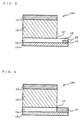
- the organic EL element disclosed in JP-A-3-262170 has the first electrode 201 which is opposed to the second electrode 203 as shown in Fig. 13, and EL emission light is taken out from either of the electrodes 201 or 203. Consequently, with regard to the light transmittance of the electrode, there are problems in that the electrode material is limited to transparent material, such as indium tin oxide (ITO) or the blue light is difficult to be effectively obtained from the electrodes 201, 203.
- ITO indium tin oxide
- the electrodes 201, 203 are composed with monocrystal semiconductor material in these organic EL elements, there is a big restriction in manufacturing. More concretely, since making such monocrystal semiconductor material is not easy, it is difficult to produce an organic EL element with a large area.
- an auxiliary electrode 213 is provided in part of the electrode 212 and the low resistance is obtained as a whole electrode.
- the transparent materials such as ITO must be used for the electrode.
- an organic light-emitting medium between either an anodic or cathodic electrode (first electrode) and a semiconductor layer comprising non-monocrystal material as well as electrically connecting the other electrode (second electrode) to the edge section of the semiconductor layer.
- an object of the present invention to provide an organic EL element that can be used for a wide variety of electrode materials and that has a large area, as well as to provide a manufacturing method that can obtain such organic EL element efficiently.
- the second electrode may be mechanically and chemically protected, and furthermore, short-circuits can be prevented and the injection of holes or electrons from the second electrode can be prevented.
- Fig. 1 is a cross-sectional view describing the construction of the organic EL element in the first embodiment.
- Fig. 2 is a cross-sectional view for describing the construction of the organic EL element in the modified example of the first embodiment (No. 1).
- Fig. 3 is a cross-sectional view for describing the construction of the organic EL element in the modified example of the first embodiment (No. 2).
- Fig. 4 is a cross-sectional view for describing the construction of the organic EL element in the modified example of the first embodiment (No. 3).
- Fig. 5 is a cross-sectional view for describing the construction of the organic EL element in the modified example of the first embodiment (No. 4).
- Fig. 6 is a cross-sectional view for describing the construction of the organic EL element in the modified example of the first embodiment (No. 5).
- Fig. 7 is a cross-sectional view for describing the construction of the organic EL element in the modified example of the first embodiment (No. 6).
- Fig. 8 is a cross-sectional view for describing the construction of the organic EL element in the modified example of the first embodiment (No. 7).
- Fig. 9 is a drawing for describing the connection structure between the second electrode and the semiconductor layer (No. 1).
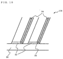
- Fig. 10 is a drawing for describing the connection structure between the second electrode and the semiconductor layer (No. 2).
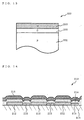
- Fig. 11 is a drawing for describing the connection structure between the second electrode and the semiconductor layer (No. 3).
- Fig. 12 is a cross-sectional view for describing a manufacturing method related to the second embodiment.
- Fig. 13 is a cross-sectional view for describing the structure of a conventional organic EL element (No. 1).
- Fig. 14 is a cross-sectional view for describing the structure of a conventional organic EL element (No. 2).
- FIG. 1 is a cross-sectional view of an organic EL element in the first embodiment, wherein on the support substrate 15, a semiconductor layer 14 comprising non-monocrystal material, an organic light-emitting medium 12, and a cathode (first cathode) 10 are formed successively.
- a semiconductor layer 14 comprising non-monocrystal material, an organic light-emitting medium 12, and a cathode (first cathode) 10 are formed successively.
- the anode (second electrode) 16 is electrically connected to the extension 18 extended in the horizontal section from the edge section 17 of the semiconductor layer 14.
- the light may be taken out from the semiconductor layer 14 to the outside by configuring in this way, the light energy (or light intensity) can be increased.
- the anode (second electrode) 16 and the cathode (first electrode) are not practically opposite to each other, a wide variety of electrode materials may be used and the electrical connection to the outside is facilitated.
- the semiconductor layer 14 is composed with the non-monocrystal material, a semiconductor layer 14 of a large area may be formed. Consequently, because it is possible to form the organic light-emitting medium 12, and the like on the semiconductor layer 14, as a result, an organic EL element 100 of a large area can be configured.
- the organic light-emitting material used for the composing material of the organic light-emitting layer preferably provides the following three functions in combination.
- the organic-light emitting material it is not always necessary for the organic-light emitting material to have all of the functions of (a) to (c) above, and for example, there are suitable ones as organic light-emitting materials of those whose hole injection transportability is far better than the electron injection transportability. Consequently, the materials that promote the electron transportation in the organic light-emitting layer and the electrons can recombine with holes in the vicinity of the center of the organic light-emitting layer can be suitably used.
- the electron mobility of the organic light-emitting material is preferably set to 1 x 10 -7 cm 2 /V ⁇ s or higher. The reason is when it becomes less than 1 x 10 -7 cm 2 /V ⁇ s, the high-speed response in the organic EL element may become difficult or the light-emitting luminance may be lowered.
- the electron mobility of the organic light-emitting material is preferably set to a value within the range of 1.1 x 10 -7 to 2 x 10 -3 cm 2 /V ⁇ s and is more suitably set to a value within the range of 1.2 x 10 -7 to 1 x 10 -3 cm 2 /V ⁇ s.
- the electron mobility is smaller than the hole mobility of the organic light-emitting material in the organic light-emitting layer. This is because if the electron mobility is reversal to this, the organic light-emitting material used for the organic light-emitting layer may be excessively limited and the light-emitting luminance may be lowered.
- the electron mobility of the organic light-emitting material is preferably greater than 1/1000 times as much as the hole mobility. This is because when the electron mobility becomes excessively small, it becomes difficult for the electron to recombine with the hole in the vicinity of the center of the organic light-emitting layer, and as a result, the light-emitting luminance may be lowered.
- the hole mobility ( ⁇ h ) and the electron mobility ( ⁇ e ) of the organic light-emitting material in the organic light-emitting layer preferably satisfy the relation of ⁇ h /2 > ⁇ e > ⁇ h /500, and more suitably satisfy the relation of ⁇ h /3 > ⁇ e > ⁇ h /100.
- aromatic cyclic compounds with a styryl group expressed by the following equations (1) to (3).
- Ar 1 denotes the aromatic group with the number of carbons ranging from 6 to 50
- Ar 2 , Ar 3 , and Ar 4 are aromatic groups with the number of carbons ranging from 6 to 50 or a hydrogen atom
- at least one of Ar 1 , Ar 2 , Ar 3 , and Ar 4 is the aromatic group
- the number of condensation n is an integer from 1 to 6.
- Ar 5 denotes the aromatic group with the number of carbons ranging from 6 to 50
- Ar6 and Ar7 are a hydrogen atom aromatic groups with the number of carbons ranging from 6 to 50 which may be replaced, and the number of condensation m is an integer from 1 to 6.
- Ar 8 and Ar 14 denote the aromatic group with the number of carbons ranging from 6 to 50
- Ar 9 through Ar 13 are a hydrogen atom or aromatic groups with the number of carbons ranging from 6 to 50 which may be replaced, and the numbers of condensation p, q, r, s are 0 or 1, respectively.
- examples of allyl group with the number of nuclear atoms ranging from 5 to 40 include phenyl, naphthyl, anthranil, phenanthryl, pyrenyl, coronyl, biphenyl, terphenyl, pyrrolyl, furanyl, thiophenyl, benzothiophenyl, oxadiazoril, diphenylanthranil, indolyl, carbazolyl, pyridyl, benzoquinolil, dibenzochrysenilene, and the like.
- Examples of preferable allylene group with the number of nuclear atoms ranging from 5 to 40 include phenylene, naphthylene, anthranilene, phenanthrylene, pyrenylene, coronylene, bipheylene, terphenylene, pyrrolylene, furanylene, thiophenylene, benzothiopheylene, oxadiazorilene, diphenylanthranilene, indolylene, carbanzolylene, pyridylene, benzoquinolilene, dibenzochryenilene, and the like.
- aromatic groups may be further replaced by different substitutes.
- preferable substitutes include alkyl group with the number of carbons from 1 to 6 (or an ethyl group, a methyl group, an i-propyl group, a n-propyl group, a s-butyl group, a t-butyl group, a pentyl group, a hexyl group, a cyclohexyl group, and the like), an alkoxy group with the number of carbons from 1 to 6 (or an ethoxyl group, a methoxyl group, an i-propoxy group, a n-propoxy group, a s-butoxy group, a t-butoxy group, a pentoxy group, a hexyloxy group, a cyclopentoxy group, a cyclohexyloxy group, and the like), an aryl group radical of the number of nuclear atoms of 5 to 40, an amino group substituted with
- benzothiazole-based compounds benzoimidazole-based compounds, benzooxyazole-based compounds, and other fluorescent brighteners compounds, styrylbenzene-based compounds, metal complexes with 8-quinolinol derivative as a ligand in combination.
- the material in combination in which the organic light-emitting material of distyryl allylene skeleton, for example, 4,4'-bis(2,2-diphenylvinyl) biphenyl, and the like is used as a host and the strong fluorescent pigments from blue to red, for example, coumarin-based fluorescent pigments or pigments similar to the host, is doped in the host.
- the organic light-emitting material of distyryl allylene skeleton for example, 4,4'-bis(2,2-diphenylvinyl) biphenyl, and the like is used as a host and the strong fluorescent pigments from blue to red, for example, coumarin-based fluorescent pigments or pigments similar to the host, is doped in the host.
- This kind of forming method is not particularly limited, but, for example, a vacuum deposition method, a spin-coating method, a casting method, a LB (Langmuir-Blodgett) method, a sputtering method, and the like may be used.
- a vacuum deposition method for example, a vacuum deposition method, a spin-coating method, a casting method, a LB (Langmuir-Blodgett) method, a sputtering method, and the like may be used.
- a vacuum deposition method it is preferable to adopt the conditions of 50-450°C for deposition temperature, in an inert gas, 1 x 10 -7 to 1 x 10 -3 Pa for vacuum, 0.01 to 50 nm/sec. for film forming rate, and 50 to 300°C for substrate temperature.
- the organic light-emitting layer it is possible to form the organic light-emitting layer by dissolving binder resins and organic light-emitting materials in a solvent to achieve the solution condition, and then forming the solution into thin film by a spin-coating method, and the like.
- the preferable binder is a transparent resin
- examples of the particularly preferable binder include polycarbonate, polystyrene, polyolefin, polyimide, polysulfone, and the like.
- the film thickness of an organic light-emitting layer there is no particular limitation to the film thickness of an organic light-emitting layer, and any film thickness may be chosen as required in accordance with conditions, but specifically, it is preferable that the film thickness is within the range of 5 nm to 5 ⁇ m. This is because when the film thickness of the organic light-emitting layer becomes less than 5 nm, the light-emitting luminance or durability may be lowered, whereas when the film thickness of the organic light emitting layer exceeds 5 ⁇ m, the value of voltage applied may be increased.
- the film thickness of the organic light-emitting layer between 10 nm and 3 ⁇ m, and more suitably between 20 nm and 1 ⁇ m.
- any material may be used except monocrystal materials.
- monocrystal materials it is desirable to use the following chalcogenide materials, non-degenerate semiconductor of metal oxides and organic semiconductor materials.
- chalcogenide materials non-degenerate semiconductor of metal oxides and organic semiconductor materials.
- organic semiconductor materials By configuring the semiconductor layer with such organic semiconductor materials, a large area can be easily obtained.
- the transparency is high and the light energy can be increased when the light is taken out from the semiconductor layer to the outside.
- At least one material chosen from a group consisting of ZnS, ZnSe, CdS, CdTe, ZnTe, MgS, MgSe, ZnSSe, ZnMgSSe, ZnCdSSe, and ZnTeSe can be mentioned.
- chalcogenide materials are ZnSSe ternary system chalcogenide materials
- chalcogenide materials are ZnMgSSe quaternary system chalcogenide materials
- acceptor materials and donor materials in the chalcogenide material and to reduce the resistance of a semiconductor layer.
- the acceptor materials referred to here are a compound added to produce the holes in the semiconductor layer, while the donor material is a compound added to produce electrons in the semiconductor layer.
- the amount of adding these acceptor materials and donor materials is not particularly limited, but specifically, it is preferable to achieve the value within the range of 0.01 to 5 mol%. The reason is that as the added amount is less than 0.01 mol%, the adding effects may not be manifested, while as such added amount exceeds 5 mol%, the materials coagulate and it becomes difficult to form a homogenous semiconductor layer. Consequently, it is more suitable to keep the amount of acceptor materials and donor materials within the range between 0.1 and 2 mol%.
- non-degenerate semiconductor of metal oxides include at least one of the material chosen from the group consisting of Al, Sn, Zn, In, Cd, Mg, and Si.
- the non-degenerate semiconductor (electric charge concentration: less than 1 x 10 20 cm -3 ) is, in general, used in the ternary or quaternary system, but by controlling the concentration of the dopant or the oxygen void, or controlling the composition ratio, it can be brought into the value within the preferable ranges of electric charge concentration and specific resistance value.
- a combination of SnO 2 and Al is generally used for a degenerate semiconductor, but by adding Al as donor impurities by 3-10 at.%, it can be made into a non-degenerate semiconductor.
- InZnO is generally used as a degenerate semiconductor, but by adding Si, Mg, Al as impurities by 1 to 20 at.%, it can be made into a non-degenerate semiconductor.
- One of the preferable organic semiconductor materials is amorphous carbon or diamond carbon.
- organic semiconductor materials may further contain hydrogen atoms or it is preferable to add boron, phosphor, or other acceptor materials or donor materials to make p-type or n-type semiconductor materials.
- the non-monocrystal material is preferably a conductive conjugate polymer, an oxidizing agent added polymer, a reducing agent added polymer, an oxidizing agent added low-molecular weight compound, or a reducing agent added low-molecular weight compound.
- polyaniline and its derivatives polythiophene and its derivatives (see JP-A-8-48858 and JP-A-7-90060)
- polymers containing aryl amine or thiophene oligomer in the main chain or the side chain can be used.
- the compounds having a nitrogen heterocyclic group are available.
- Examples of an oxidizing agent added to polymers and a low-molecular weight compounds include Lewis acid, for example, iron chloride, antimony chloride, aluminum chloride, and the like.
- examples of a reducing agent added to polymers and a low-molecular weight compounds include alkaline earth metal, rare earth metals, alkali compounds, alkali earth compounds, rare earth compounds, and the like.
- the organic complex (the ligand is an organic material) of alkali metals or alkali earth metals mentioned above are included.
- the light transmittance of the semiconductor layer is preferably 10% or higher, more preferably 50% or higher, and more suitably 70% or higher.
- the band gap is preferably 2.7 eV or greater.
- the electric charge concentration in the semiconductor layer is preferably kept to the range from 1 x 10 12 to 1 x 10 20 cm -3 .
- the reason is that when the electric charge concentration of the semiconductor layer becomes less than 1 x 10 12 cm -3 , the drive voltage becomes remarkably high and light luminance may become non-uniform, while when the electric charge concentration of the semiconductor layer becomes higher than 1 x 10 20 cm -3 , the metal-like property of the semiconductor layer occurs and the excited condition generated in the organic light-emitting medium may be likely to be quenched.
- the electric charge concentration of the semiconductor layer is preferably kept to the range from 1 x 10 13 to 1 x 10 19 cm -3 and more suitably to the range from 1 x 10 14 to 1 x 10 18 cm -3 .
- the specific resistance of the semiconductor layer is preferably held to the range from 1 x 10 -3 to 1 x 10 9 ⁇ ⁇ cm. This is because when the specific resistance of the semiconductor layer becomes less than 1 x 10 -3 ⁇ ⁇ cm, the metal-like property occurs, and the excited condition generated in the organic light-emitting medium may be likely to be quenched, while when the specific resistance of the semiconductor layer becomes higher than 1 x 10 9 ⁇ ⁇ cm, the drive voltage may become excessively high.
- pixels of organic EL element of typical size (for example, 300 ⁇ m x 300 ⁇ m) is formed and driven by d. c.
- the specific resistance of the semiconductor layer is more preferably held to the range from 1 x 10 -3 to 1 x 10 5 ⁇ ⁇ cm. By keeping the specific resistance of the semiconductor layer to this range, still more uniform luminescence may be obtained.
- the specific resistance of the semiconductor layer is more preferably held to the range from 1 x 10 -3 to 1 x 10 4 ⁇ ⁇ cm. By keeping the specific resistance of the semiconductor layer to this range, large current may be passed in a specified time in accordance with the duty ratio.
- the film thickness of the semiconductor layer should be a value within the range from 1 to 700 nm. The reason is that when the film thickness of the semiconductor layer is less than 1 nm, the continuous film can not be obtained, while when the film thickness of the semiconductor layer is more than 700 nm, the light take-out efficiency may be lowered.
- the film thickness of the semiconductor layer is more preferably between 5 and 500 nm and more suitably between 10 and 300 nm.
- the anode and the cathode are not practically opposite to each other and the light is able to be taken out from the semiconductor layer to the outside, the restrictions to kinds from the viewpoint of light transmittance, and the like can be remarkably reduced.
- either one of these anode and cathode is designated as the first electrode and the other as the second electrode. Consequently, it is possible to designate the first electrode as the anode and the second electrode as the cathode, or the first electrode as the cathode and the second electrode as the anode.
- examples of the materials used for the electrodes are enumerated, but various kinds of metals and electrically conductive compounds may be used for the second electrode if the injection to the semiconductor layer is able to be successfully carried out.
- metal, alloy, electrically conductive compound or these mixtures with a large work function (for example, 4.0 eV or more).
- a large work function for example, 4.0 eV or more.
- ITO indium tin oxide
- IZO indium zinc oxide
- zinc oxide gold, platinum, palladium, and the like
- gold, platinum, palladium, and the like can be used independently in one kind or in two or more kinds in the combination.
- the film thickness of the anode is not particularly limited, but it is preferably between 10 and 1,000 nm and more suitably between 10 and 200 nm.
- metal, alloy, electrically conductive compound or these mixtures with a small work function (for example, less than 4.0 eV).
- a small work function for example, less than 4.0 eV.
- magnesium, aluminum, indium, lithium, sodium, silver, tungsten, tantalum-tungsten alloy, titanium, chromium, aluminum-tungsten alloy, aluminum-titanium alloy, and the like can be used independently in one kind or in two or more kinds in the combination.
- the film thickness of the cathode is not particularly limited, either, but it is preferably between 10 and 1,000 nm and more suitably between 10 and 200 nm.
- the electrical connection referred to here is the connection that enables electrical conduction by connecting or bringing either anode or cathode to or in contact with the semiconductor layer. Consequently, the contact resistance should be brought preferably to 1 k ⁇ or lower, and more suitably to 100 ⁇ or lower.
- the location and connection structure of the second electrode in the present invention should not be limited to the locations indicated in Figs. 1 to 11, and may be a combination of these structures, and the like as required, and if it is the location that enables electrical connection with the edge section of the semiconductor layer, any locations other than illustrated may be acceptable.
- Fig. 1 indicates the location of the second electrode 16 in the organic EL element 100 of the first embodiment, and a recessed section 20 is provided in the extension 18 extended in the horizontal direction from the edge section 17 of the semiconductor layer 14, and in this recessed section 20, an anode (second electrode) 16 is formed.
- Forming the second electrode 16 at this kind of position makes it possible to bring the electrically connected section between the second electrode 16 and the semiconductor layer 14 in a large area, prevents occurrence of short-circuiting, and in addition, facilitate the electrical connection with the outside. Furthermore, forming the second electrode 16 at this kind of position aligns the top surface of the second electrode 16 to the top surface of the semiconductor layer 14 to be flat, and makes it possible to easily to carry out the treatment such as insulation, and the like.
- Fig. 2 shows the location of the second electrode 16 in the organic EL element 102 of the modification example (No. 1) of the first embodiment, and an anode (second electrode) 16 is formed on the surface of an extension 18 which is extended in the horizontal direction from the edge section 17 of the semiconductor layer 14.
- Forming the second electrode 16 at this kind of location can make the electrically connected section between the second electrode 16 and the semiconductor layer 14 larger.
- the distance between the second electrode 16 and the organic light-emitting medium 12 can be made longer, occurrence of short-circuiting is able to be effectively prevented.
- the first electrode 10 and the second electrode 16 are aligned in the same direction and the top surface direction is exposed in Fig. 2, electrical connection with the outside is made easy by using this.
- Fig. 3 shows the location of the second electrode 16 in the organic EL element 104 of the modified example (No. 2) of the first embodiment, in which there is the extension 18 extended in the horizontal direction from the edge section 17 of the semiconductor layer 14, and the second electrode 16 is formed on the side opposite to the side to which the organic light-emitting medium 12 is located.
- Forming the second electrode 16 at this kind of location can make the electrically connected section between the second electrode 16 and the semiconductor layer 14 larger, and occurrence of short-circuits is able to be effectively prevented between the second electrode and the organic light-emitting medium 12 without providing electrical insulation treatment.
- an recessed section 22 is provided in the extension 18, in which the second electrode 16 is formed.
- Fig. 4 shows the location of the second electrode 16 in the organic EL element 106 of the modified example (No. 3) of the first embodiment. It shows that the second electrode 16 is directly formed to the edge section (side end) 17 of the semiconductor layer.
- Forming the second electrode 16 at this kind of location can make the configuration of the organic EL element 106 in the lateral direction.
- Fig. 5 shows a modification example (No. 4) of the first embodiment, and shows an example in which the second electrodes 16, 23 are provided in two places in the organic EL elements 112. That is, it indicates that the second electrodes 16, 23 are formed via the extension 18 to the edge section (side end) 17 on both sides of the semiconductor layer 14.
- Forming a plurality of second electrodes 16, 23 in this way can increase the contact area of these second electrodes 16, 23 with the extension 18 in the semiconductor layer 14, facilitating the injection of electrons and holes. Even when continuity failure occurs between either of the two electrodes 16, 23 and the extension 18 in the semiconductor layer 14, continuity with the other extended section 18 in the semiconductor layer 14 can be maintained with the other second electrode 16, 23.
- Fig. 6 shows a modified example (No. 5) of the first embodiment, in which a taper 24 is formed at the edge section of the semiconductor layer 14, and on the taper, the second electrode 16 is formed.
- Forming the semiconductor layer 14 and the second electrode 16 in the form of taper in this way can make the contact area larger and facilitate injection of electrons and holes.
- the taper 24 is formed descending in the right in Fig. 6, but conversely, this may be formed ascending in the right.
- the cross-sectional profile in the taper 24 is formed in a triangle in Fig. 6, but this cross-sectional profile may be a trapezoid.
- Fig. 7 shows a modified example (No. 6) of the first embodiment, in which the semiconductor layer 9 is provided on the first electrode 10 side. That is, it shows that the first electrode 10 is formed at the edge section on the side end of the semiconductor layer 9.
- Forming the first electrode 10 in this way eliminates the restriction to the kinds for the first electrode, while since opaque low-resistance material may be used, injection of electrons and holes becomes easier.
- Fig. 8 shows the modified example (No. 7) of the first embodiment, in which steps are formed at the edge section of the semiconductor layer 14, and on the step, the conductive layer 25 is formed, and on the conductive layer 25, the second electrode 16 is formed.
- Bringing the semiconductor layer 14 to the second electrode in the form of steps and further forming the conductive layer 25 can increase the contact area and facilitates the lowering of resistance.
- Fig. 9 shows the connection condition and connection position of the semiconductor layer 14 and the second electrode 16.
- Fig. 9 (a) and (b) show plans, while Fig. 9 (c) and (d) show cross-sectional views.
- the head end section of the semiconductor layer 14 can be split as shown in Fig. 9 (a) or the head end section of the semiconductor layer 14 can be made into a hole structure as shown in Fig. 9 (b).
- a recessed section is provided at the head end section of the semiconductor layer 14 or a triangle is formed at the head end section of the semiconductor layer 14 as shown in Fig. 9 (d).
- Fig. 10 shows the location of the second electrode 34 in the organic EL element 108 of the modified example (No. 8) of the first embodiment, indicating the condition with the organic light-emitting medium, the first electrode, and the like omitted.
- a plurality of second electrodes 34 are patterned and installed in the form of stripes.
- a plurality of semiconductor layers 32 are patterned and installed along the second electrode 34.
- the second electrode 34 is electrically connected along the edge section (side end) 36 of the semiconductor layer 32.
- forming the second electrode 34 in this kind of location can effectively prevent voltage drop by the resistance at the semiconductor layer 32 (not illustrated) by applying voltage across the first electrode (not illustrated) and the second electrode 34.
- the organic EL element (pixels) 108 can be arranged in the matrix form. Consequently, a large volume of the light energy can be taken out from the light-emitting surface of the large-area semiconductor layer 32, and at the same time, a thin-type display device can be presented.
- Fig. 11 shows the position of the second electrode 40 in the organic EL element 110 of the modified example (No. 9) of the first embodiment.
- Fig. 11 (a) indicates planely that the second electrode 40 is patterned in the form of lattices on the support substrate 42
- Fig. 11 (b) indicates cross-sectionally that the semiconductor layer 44 is installed as if it covers the second electrode 40 and partly exposed support substrate 42.
- Fig. 11 (c) shows cross-sectionally that in the organic EL element 110 in which the organic light-emitting medium 46 is formed on the all over the semiconductor layer 44 shown in Fig. 11 (b), above which the patterned first electrode 48 is formed, the light is taken out from the section shown with symbol "T" to the outside.
- the second electrode 40 in this kind of location can make the electrically connected section between the second electrode 40 and the semiconductor layer 22 be a large area, and the voltage drop caused by the resistance at the semiconductor layer can be effectively prevented.
- the organic EL element (pixels) 110 can be arranged in a matrix by the positional relationship with the first electrode (not illustrated). And a large volume of light may be taken out from the light-emitting surface of the large-area semiconductor layer 44.
- the second electrode may be included in one pixel and the above-mentioned configuration may be included in the semiconductor layer.
- the configuration shown in Fig. 11 may be two-dimensionally arranged as dots (part of the pixel) and may be formed in a matrix.
- the support substrate 15 in the organic EL element provides excellent mechanical strength and less permeability of moisture and oxygen
- the support substrate which is generally used for this kind of an organic EL element can be used as it is.
- glass substrates, ceramic substrates, and the like 100 to 2,000 ⁇ m thick can be mentioned.
- the light transmittance of the relevant support substrate is preferably 90% or more, and suitably 93% or more, and more preferably 98% or more.
- the organic EL element of the first embodiment has the anode designated as the second electrode and the cathode as the first electrode, and virtually has the configuration of (i), but taking the configurations of the organic EL element of (ii) through (iv) is preferable by combining other component elements, such as hole injection layer or electron injection layer.
- semiconductor layer (+ anode (second electrode)) means that an anode which is not opposite to a cathode is provided with a semiconductor layer.
- Fig. 12(a)-(d) is illustrations that schematically show the organic EL element in each process(step) of the manufacturing method related to the second embodiment.
- the manufacturing method of the organic EL element is focused, and with respect to the component materials, and the like, the contents described for the first embodiment may apply.
- Fig. 12(a) shows the condition in which the anode (second electrode) 16 is installed on the support substrate 15.
- the method for forming this anode 16 is not particularly limited, but the anode may be able to be formed in the specified location by combining sputtering (deposition method) and photolithography. Specifically, on the support substrate 15, the anode layer is formed on the whole surface by the use of sputtering, and then, by using photolithography, patterns are formed and the anode 16 is accurately formed at the position which is electrically connected to the edge section 17 of the semiconductor layer 14 in the future.
- forming the anode in this manner enables accurate electrical connection with the edge section of the semiconductor layer when the semiconductor layer is formed in the subsequent (step).
- forming the anode in this manner embeds the anode in the electrically insulated support substrate and can definitely maintain the electrical insulation with the organic light-emitting medium to be formed in the subsequent process(step) without using any electrically insulating material.
- Fig. 12(b) shows the condition in which the semiconductor layer 14 is installed adjacent to the anode (second electrode) 16 on the support substrate 15. That is, the figure shows the condition in which the semiconductor layer 14 is installed ready for electrical connection at the end section 17.
- the method for forming this semiconductor layer 14 is not particularly limited, but for example, the semiconductor layer 14 is able to be formed at the specified location by sputtering (deposition) following the preceding process(steps). That is, after etching the anode layer in the preceding procedure, the resist is separated and the semiconductor layer 14 is formed on the whole surface and patterns are provided by photolithography method, thereby forming the semiconductor layer 14 at the specified location easily and in a short time.
- the semiconductor layer 14 is formed partly overlapping with the anode 16, for example, the semiconductor layer 14 is formed with the recessed section 22 provided as shown in Fig. 3, it is also preferable to form the semiconductor layer 14 at the specified location by further using photolithography.
- Fig. 12(c) shows the condition in which the organic light-emitting medium 12 is installed on the semiconductor layer 14.
- the method of forming this organic light-emitting medium is not particularly limited, but for example, the organic light-emitting medium may be formed at the specified location by the use of a shadow mask at the time of deposition.
- the organic light-emitting medium 12 is composed with the light-emitting layer, hole transport layer, hole injection layer, intermediate interface layer, and the like, each layer is able to be accurately formed by repeating the deposition process each time.
- the organic light-emitting medium 12 when the organic light-emitting medium 12 is formed, it is preferably to coat the anode by providing the electrical insulation layer (not illustrated). By forming the electrical insulation layer in this manner, the electrical insulation between the anode and the organic light-emitting medium can be accurately secured. Consequently, occurrence of short-circuits and the cross-talking can be effectively prevented.
- This kind of electrical insulation layer is preferably composed with, for example, photo-curing type epoxy resin, acrylic resin, siloxane resin, and the like.
- photo-curing type epoxy resin acrylic resin, siloxane resin, and the like.
- acrylic resin acrylic resin
- siloxane resin siloxane resin
- metallic layer for example, non-charge injection type semiconductor layer and metallic layer are mentioned.
- Fig. 12(d) shows the condition in which the cathode (first electrode) 10 is installed on the organic light-emitting medium 12 and the organic EL element 106 is configured.
- This cathode (first electrode) 10 can also be formed at the specified location by combining, for example, sputtering (deposition) and photolithography as described above.
- the semiconductor layer 14 is formed after forming the anode 16, but it is also preferable to form the semiconductor layer and the anode in the procedure reversal to this. That is, by forming the semiconductor layer 14 first, and then forming the anode 16, for example, the organic EL elements 100, 102, 108 can be easily fabricated as shown in Fig. 1, Fig. 2, and Fig. 10.
- the second electrode is formed on the substrate, the first electrode is formed on the substrate and then the organic light-emitting medium semiconductor layer is formed; then, the second electrode may be formed at the edge section of the semiconductor layer.
- a transparent glass substrate having a dimension of 1.1 mm(thickness) ⁇ 200 mm (length) ⁇ 200 mm (width) was ultrasonically cleaned and after drying in the N 2 (nitrogen gas) environment, the glass substrate was cleaned by the use of UV (ultraviolet ray) and ozone further for 10 minutes. Then, on the cleaned glass substrate, a thin film (100 nm thick) comprising Al/Si alloy (Si concentration: 1 at.%) was formed by the use of the sputtering apparatus (available from ULVAC JAPAN, Ltd.).
- This Al/Si alloy thin film was patterned in lattices (line width: 20 ⁇ m; lattice pitch: 320 ⁇ m) by the use of photolithography as shown in Fig. 11(a).
- the construction of the configuration in which the cathode (second electrode) was electrically connected at the edge section of the semiconductor layer was intended.
- the glass substrate on which the cathode was formed was cleaned with argon plasma, and then, on this glass substrate, using the vacuum deposition apparatus (available from ULVAC JAPAN, Ltd.), ZnSe and ZnCl 2 with 150 nm film thickness are simultaneously deposited to form the n-type semiconductor layer.
- ZnSe deposition was carried out at the vacuum of 1 x 10 -6 Torr (1.33 x 10 -4 Pa) and at the temperature of 760 to 780°C, and ZnCl 2 deposition was carried out so that the specific resistance of the semiconductor layer satisfied 3 x 10 3 ⁇ ⁇ cm.
- the charge concentration of the semiconductor layer was measured by the four-terminal method and it was confirmed that the charge concentration is 5 x 10 15 cm -3 .
- Alq functions as a light-emitting layer
- NPD as a hole transport layer
- TPD74 as a hole injection layer
- CuPc as an intermediate interface layer
- the Al/Si alloy thin film patterned in the form of lattices (line width: 20 ⁇ m; lattice pitch: 320 ⁇ m) was formed and designated it as the anode (second electrode).
- the glass substrate with the anode formed was cleaned with argon plasma, and then, on this glass substrate, using the vacuum deposition apparatus (available from ULVAC JAPAN, Ltd.), CdS and Cu are simultaneously deposited in 30 nm film thickness to form the p-type semiconductor layer.
- the deposition was carried out at the vacuum of 1 x 10 -6 Torr (1.33 x 10 -4 Pa). and at the substrate temperature of 160°C, and Cu deposition was carried out so that the specific resistance of the semiconductor layer satisfied 2 x 10 ⁇ ⁇ cm.
- the charge concentration of the semiconductor layer was measured by the four-terminal method and it was confirmed that the charge concentration is 4 x 10 17 cm -3 .
- the semiconductor layer obtained that comprised a combination of CdS and Cu was separately confirmed to provide the properties as the p-type semiconductor.
- TPD74, NPD, and Alq used in Example 1 were deposited successively to form the organic light-emitting medium with each film thickness of 200 nm, 20 nm, and 60 nm, respectively.
- TPD74 functions as a hole injection layer
- NPD as a hole transport layer
- Alq as a light-emitting layer
- Example 3 effects of the organic semiconductor layer were investigated. That is, in place of the semiconductor layer comprising a combination of CdS and Cu in Example 2, a 70-nm-film thickness semiconductor layer comprising PEDOT (3,4-polyethylene dioxythiophene, available from Bayer), which is polymer indicating semiconductance, was spin-coated in the condition of the aqueous solution, and then, was vacuum-dried to form an organic EL element, with others all same as Example 2.
- PEDOT polyethylene dioxythiophene
- the organic EL element was fabricated in the same manner as Example 1, with an exception of not forming the patterned (line width: 20 ⁇ m; lattice pitch: 320 ⁇ m) Al/Si alloy thin film (cathode).
- the organic EL element was fabricated in the same manner as Example 1, with an exception of not patterning in lattices the Al/Si alloy thin film (cathode) in Example 1 but forming the film throughout the whole surface.
- Example 1 Example 2
- Example 3 Comparative example 1 Comparative example 2
- Second electrode Patterned cathode Patterned anode Patterned anode
- Non-None patterned cathode Semi-conductor layer ZnSe/ZnCl 2 CdS/Cu PEDOT ZnSe/ZnCl 2 ZnSe/ZnCl 2
- EL light emission take-out surface
- Semi-conductor layer Semi-conductor layer
- Semi-conductor layer Semi-conductor layer
- Half-life (hours) 480 620 790 0 0
- the first electrode and the second electrode were no longer necessary to be brought virtually opposite to each other by installing an organic light emitting medium between the first electrode (anode or cathode) and the semiconductor layer comprising the non-monocrystal material and electrically connecting the second electrode (cathode or anode) to the edge section of the semiconductor layer. Consequently, the following effects have been able to be obtained.
- the selectivity of order of each forming process(step) has become increased by including a step for the second electrode, a step for forming the semiconductor layer at the position connectable to the second electrode edge section by the use of non-monocrystal material, a step for forming the organic light-emitting medium, and a step for forming the first electrode. Because the non-monocrystal material is used for the semiconductor layer, an organic EL element which provides uniform properties and a large area are able to be easily manufactured. In addition, since there is no need to form the first electrode and the second electrode opposite to each other, the light energy take out is able to be increased, and at the same time, a wide variety of electrode materials have been able to be used.
Landscapes
- Physics & Mathematics (AREA)
- Optics & Photonics (AREA)
- Electroluminescent Light Sources (AREA)
Priority Applications (1)
| Application Number | Priority Date | Filing Date | Title |
|---|---|---|---|
| EP10156317A EP2202822A3 (en) | 1999-04-30 | 2000-04-27 | Organic electroluminescence element and manufacturing method thereof |
Applications Claiming Priority (3)
| Application Number | Priority Date | Filing Date | Title |
|---|---|---|---|
| JP12447799 | 1999-04-30 | ||
| JP12447799 | 1999-04-30 | ||
| PCT/JP2000/002796 WO2000067531A1 (fr) | 1999-04-30 | 2000-04-27 | Dispositif organique electroluminescent et procede de fabrication |
Publications (1)
| Publication Number | Publication Date |
|---|---|
| EP1111967A1 true EP1111967A1 (en) | 2001-06-27 |
Family
ID=14886496
Family Applications (2)
| Application Number | Title | Priority Date | Filing Date |
|---|---|---|---|
| EP10156317A Withdrawn EP2202822A3 (en) | 1999-04-30 | 2000-04-27 | Organic electroluminescence element and manufacturing method thereof |
| EP00922898A Withdrawn EP1111967A1 (en) | 1999-04-30 | 2000-04-27 | Organic electroluminescent device and method of manufacture thereof |
Family Applications Before (1)
| Application Number | Title | Priority Date | Filing Date |
|---|---|---|---|
| EP10156317A Withdrawn EP2202822A3 (en) | 1999-04-30 | 2000-04-27 | Organic electroluminescence element and manufacturing method thereof |
Country Status (7)
| Country | Link |
|---|---|
| US (3) | US6856089B2 (ko) |
| EP (2) | EP2202822A3 (ko) |
| JP (2) | JP4864207B2 (ko) |
| KR (1) | KR100722084B1 (ko) |
| CN (1) | CN100356608C (ko) |
| TW (1) | TW463392B (ko) |
| WO (1) | WO2000067531A1 (ko) |
Cited By (4)
| Publication number | Priority date | Publication date | Assignee | Title |
|---|---|---|---|---|
| WO2002095841A3 (en) * | 2001-05-18 | 2003-03-06 | Univ Cambridge Tech | Electroluminescent device |
| WO2008023008A1 (de) * | 2006-08-24 | 2008-02-28 | Osram Opto Semiconductors Gmbh | Flächiges leuchtelement sowie verwendung des flächigen leuchtelementes |
| US7393600B2 (en) | 2002-08-02 | 2008-07-01 | Idemitsu Kosan Co., Ltd. | Sputtering target, sintered article, conductive film fabricated by utilizing the same, organic EL device, and substrate for use therein |
| EP2557899A4 (en) * | 2010-04-05 | 2015-10-21 | Konica Minolta Holdings Inc | TRANSPARENT ELECTRODE AND ORGANIC ELECTRONIC ELEMENT THEREOF |
Families Citing this family (36)
| Publication number | Priority date | Publication date | Assignee | Title |
|---|---|---|---|---|
| KR100702763B1 (ko) * | 1999-02-15 | 2007-04-03 | 이데미쓰 고산 가부시키가이샤 | 유기 전자 발광 소자 및 그의 제조 방법 |
| JP4864207B2 (ja) * | 1999-04-30 | 2012-02-01 | 出光興産株式会社 | 有機エレクトロルミネッセンス素子およびその製造方法 |
| EP1096568A3 (en) * | 1999-10-28 | 2007-10-24 | Sony Corporation | Display apparatus and method for fabricating the same |
| US7301276B2 (en) * | 2000-03-27 | 2007-11-27 | Semiconductor Energy Laboratory Co., Ltd. | Light emitting apparatus and method of manufacturing the same |
| JP2004063363A (ja) * | 2002-07-31 | 2004-02-26 | Semiconductor Energy Lab Co Ltd | 電界発光素子用材料、およびそれを用いた電界発光素子 |
| TWI282701B (en) * | 2002-08-16 | 2007-06-11 | Au Optronics Corp | Organic electroluminescent device |
| US20040252488A1 (en) * | 2003-04-01 | 2004-12-16 | Innovalight | Light-emitting ceiling tile |
| KR100657891B1 (ko) * | 2003-07-19 | 2006-12-14 | 삼성전자주식회사 | 반도체 나노결정 및 그 제조방법 |
| JP4689176B2 (ja) * | 2004-02-26 | 2011-05-25 | 大日本印刷株式会社 | 有機エレクトロルミネッセンス素子 |
| US7750352B2 (en) * | 2004-08-10 | 2010-07-06 | Pinion Technologies, Inc. | Light strips for lighting and backlighting applications |
| JP4837958B2 (ja) * | 2005-08-26 | 2011-12-14 | 大日本印刷株式会社 | 有機エレクトロルミネッセンス素子 |
| KR101254560B1 (ko) | 2006-06-29 | 2013-04-19 | 엘지디스플레이 주식회사 | 유기전계 발광소자와 그 제조방법 |
| JP4832250B2 (ja) | 2006-10-23 | 2011-12-07 | Hoya株式会社 | p型半導体材料、半導体素子、有機エレクトロルミネッセンス素子、及びp型半導体材料の製造方法 |
| US8697254B2 (en) * | 2006-11-14 | 2014-04-15 | Sri International | Cavity electroluminescent devices and methods for producing the same |
| KR100785037B1 (ko) * | 2006-12-13 | 2007-12-12 | 삼성전자주식회사 | GaInZnO 다이오드 |
| KR101612130B1 (ko) * | 2007-03-20 | 2016-04-12 | 이데미쓰 고산 가부시키가이샤 | 스퍼터링 타겟, 산화물 반도체막 및 반도체 디바이스 |
| US20080309225A1 (en) * | 2007-05-18 | 2008-12-18 | Masao Shimizu | Organic electroluminescent display device |
| KR20100076950A (ko) | 2007-08-23 | 2010-07-06 | 에스알아이 인터내셔널 | 유기 음극을 사용하는 전장발광 장치 |
| EP2238635B1 (en) * | 2008-01-24 | 2012-07-04 | SRI International | High efficiency electroluminescent devices and methods for producing the same |
| WO2010044584A2 (ko) * | 2008-10-13 | 2010-04-22 | Choi Woon Yong | 리던던시 전극을 갖는 엘이디 어셈블리 및 그 제조 방법 |
| JPWO2010119503A1 (ja) * | 2009-04-14 | 2012-10-22 | シャープ株式会社 | 有機エレクトロルミネッセンス素子およびその製造方法 |
| JP4907714B2 (ja) * | 2009-11-16 | 2012-04-04 | 大日本印刷株式会社 | 有機エレクトロルミネッセンス素子 |
| KR101074804B1 (ko) * | 2009-11-24 | 2011-10-19 | 한국과학기술원 | 유기 발광 소자, 이를 포함하는 조명장치, 및 이를 포함하는 유기 발광 디스플레이 장치 |
| US8421064B2 (en) * | 2010-04-09 | 2013-04-16 | Electronics And Telecommunications Research Institute | Organic-light-emitting-diode flat-panel light-source apparatus |
| WO2011148931A1 (ja) * | 2010-05-28 | 2011-12-01 | コニカミノルタホールディングス株式会社 | 有機電子デバイス用電極 |
| EP2613611A4 (en) | 2010-09-01 | 2014-07-30 | Showa Denko Kk | ELECTROLUMINESCENCE ELEMENT, DISPLAY DEVICE AND LIGHTING DEVICE |
| CN103250265B (zh) * | 2011-05-20 | 2016-03-16 | 松下知识产权经营株式会社 | 有机电致发光元件 |
| JPWO2013129612A1 (ja) | 2012-02-29 | 2015-07-30 | 昭和電工株式会社 | エレクトロルミネッセント素子の製造方法 |
| US20150102307A1 (en) | 2012-02-29 | 2015-04-16 | Showa Denko K.K. | Electroluminescent element, method for manufacturing electroluminescent element, display device, and illumination device |
| JPWO2013129611A1 (ja) | 2012-02-29 | 2015-07-30 | 昭和電工株式会社 | エレクトロルミネッセント素子の製造方法 |
| CN103296220A (zh) * | 2012-03-02 | 2013-09-11 | 群康科技(深圳)有限公司 | 串接型有机电致发光模块 |
| KR101376732B1 (ko) * | 2012-09-19 | 2014-04-07 | 전자부품연구원 | 다층 전이금속 칼코겐화합물을 이용한 투명전자소자, 이를 이용한 광전자 소자 및 트랜지스터 소자 |
| JP5723344B2 (ja) | 2012-09-25 | 2015-05-27 | 株式会社東芝 | 有機電界発光素子および発光装置 |
| JPWO2015182130A1 (ja) * | 2014-05-30 | 2017-04-20 | 株式会社Joled | 有機el素子及び有機el発光装置 |
| CN106898625B (zh) * | 2015-12-18 | 2020-06-02 | 中芯国际集成电路制造(上海)有限公司 | 图像传感器芯片的封装结构及封装方法 |
| CN107507815A (zh) * | 2016-06-14 | 2017-12-22 | 中芯国际集成电路制造(上海)有限公司 | 焊垫结构及csp封装方法 |
Citations (1)
| Publication number | Priority date | Publication date | Assignee | Title |
|---|---|---|---|---|
| JPH1039792A (ja) * | 1996-07-19 | 1998-02-13 | Hokuriku Electric Ind Co Ltd | El素子とその製造方法 |
Family Cites Families (31)
| Publication number | Priority date | Publication date | Assignee | Title |
|---|---|---|---|---|
| WO1983004123A1 (en) * | 1982-05-19 | 1983-11-24 | Matsushita Electric Industrial Co., Ltd. | Electroluminescent display unit |
| JPS6012696A (ja) * | 1983-07-04 | 1985-01-23 | 日本電気株式会社 | 薄膜エレクトロルミネツセンス素子 |
| US5229628A (en) * | 1989-08-02 | 1993-07-20 | Nippon Sheet Glass Co., Ltd. | Electroluminescent device having sub-interlayers for high luminous efficiency with device life |
| US5128587A (en) * | 1989-12-26 | 1992-07-07 | Moltech Corporation | Electroluminescent device based on organometallic membrane |
| EP0440957B1 (de) | 1990-02-08 | 1996-03-27 | Bayer Ag | Neue Polythiophen-Dispersionen, ihre Herstellung und ihre Verwendung |
| JPH03262170A (ja) * | 1990-03-13 | 1991-11-21 | Toshiba Corp | 有機/無機接合型半導体素子 |
| JPH0414215A (ja) * | 1990-05-08 | 1992-01-20 | Nkk Corp | 半導体薄膜及びその製造方法 |
| JPH05307997A (ja) * | 1992-04-30 | 1993-11-19 | Pioneer Electron Corp | 有機エレクトロルミネッセンス素子 |
| US5652067A (en) * | 1992-09-10 | 1997-07-29 | Toppan Printing Co., Ltd. | Organic electroluminescent device |
| JPH0696862A (ja) * | 1992-09-14 | 1994-04-08 | Fuji Xerox Co Ltd | 無機薄膜el素子 |
| EP0686662B2 (de) | 1994-05-06 | 2006-05-24 | Bayer Ag | Leitfähige Beschichtungen |
| JPH08180974A (ja) | 1994-12-26 | 1996-07-12 | Nippondenso Co Ltd | El素子およびその製造方法 |
| EP0771459A2 (en) * | 1995-05-19 | 1997-05-07 | Koninklijke Philips Electronics N.V. | Display device |
| JPH10503165A (ja) * | 1995-05-19 | 1998-03-24 | フィリップス エレクトロニクス ネムローゼ フェンノートシャップ | 未硬化セラミック成形部材を焼結する方法及び炉 |
| TW364275B (en) * | 1996-03-12 | 1999-07-11 | Idemitsu Kosan Co | Organic electroluminescent element and organic electroluminescent display device |
| US6433355B1 (en) * | 1996-06-05 | 2002-08-13 | International Business Machines Corporation | Non-degenerate wide bandgap semiconductors as injection layers and/or contact electrodes for organic electroluminescent devices |
| US5739545A (en) * | 1997-02-04 | 1998-04-14 | International Business Machines Corporation | Organic light emitting diodes having transparent cathode structures |
| JP3526877B2 (ja) * | 1997-03-11 | 2004-05-17 | ジィ、オハイオ、ステイト、ユニバーシティー、リサーチ、ファンデーション | 色可変バイポーラ/ac発光素子 |
| JPH1131590A (ja) * | 1997-07-09 | 1999-02-02 | Tdk Corp | 有機el素子 |
| KR19990014304A (ko) * | 1997-07-30 | 1999-02-25 | 아사구사 나오유끼 | 반도체 레이저, 반도체 발광 소자 및 그 제조 방법 |
| GB9718393D0 (en) * | 1997-08-29 | 1997-11-05 | Cambridge Display Tech Ltd | Electroluminescent Device |
| US6069442A (en) * | 1997-09-18 | 2000-05-30 | Eastman Kodak Company | Organic electroluminescent device with inorganic electron transporting layer |
| KR100517851B1 (ko) * | 1997-10-15 | 2005-10-04 | 도레이 가부시끼가이샤 | 유기 전계 발광 장치 |
| JPH11144877A (ja) * | 1997-11-10 | 1999-05-28 | Fuji Electric Co Ltd | 有機発光素子 |
| JP4837811B2 (ja) * | 1998-04-09 | 2011-12-14 | 出光興産株式会社 | 有機エレクトロルミネッセンス素子 |
| EP0996116B1 (en) * | 1998-04-13 | 2007-06-20 | Seiko Epson Corporation | Information recording method and an information recording device |
| JP2000091083A (ja) * | 1998-09-09 | 2000-03-31 | Sony Corp | 有機elディスプレイ |
| US6351067B2 (en) * | 1999-01-21 | 2002-02-26 | City University Of Hong Kong | Organic electroluminescent device with improved hole injecting structure |
| KR100694959B1 (ko) * | 1999-04-02 | 2007-03-14 | 이데미쓰 고산 가부시키가이샤 | 유기 전기 발광 디스플레이 장치 및 그의 제조 방법 |
| US6525466B1 (en) * | 1999-04-09 | 2003-02-25 | Arizona Board Of Regents On Behalf Of The University Of Arizona | Cathode including a mixture of a metal and an insulator for organic devices and method of making the same |
| JP4864207B2 (ja) * | 1999-04-30 | 2012-02-01 | 出光興産株式会社 | 有機エレクトロルミネッセンス素子およびその製造方法 |
-
2000
- 2000-04-27 JP JP2000614781A patent/JP4864207B2/ja not_active Expired - Lifetime
- 2000-04-27 EP EP10156317A patent/EP2202822A3/en not_active Withdrawn
- 2000-04-27 KR KR1020007015073A patent/KR100722084B1/ko active IP Right Grant
- 2000-04-27 EP EP00922898A patent/EP1111967A1/en not_active Withdrawn
- 2000-04-27 WO PCT/JP2000/002796 patent/WO2000067531A1/ja active Application Filing
- 2000-04-27 CN CNB008010803A patent/CN100356608C/zh not_active Expired - Lifetime
- 2000-04-29 TW TW089108193A patent/TW463392B/zh not_active IP Right Cessation
-
2001
- 2001-01-02 US US09/750,682 patent/US6856089B2/en not_active Expired - Lifetime
-
2004
- 2004-12-30 US US11/024,729 patent/US6998773B2/en not_active Expired - Lifetime
-
2005
- 2005-11-14 US US11/272,069 patent/US7423371B2/en not_active Expired - Fee Related
-
2010
- 2010-04-12 JP JP2010091306A patent/JP4594446B2/ja not_active Expired - Lifetime
Patent Citations (1)
| Publication number | Priority date | Publication date | Assignee | Title |
|---|---|---|---|---|
| JPH1039792A (ja) * | 1996-07-19 | 1998-02-13 | Hokuriku Electric Ind Co Ltd | El素子とその製造方法 |
Non-Patent Citations (2)
| Title |
|---|
| KIM H ET AL: "Electrical, optical, and structural properties of indium-tin-oxide thin films for organic light-emitting devices", JOURNAL OF APPLIED PHYSICS, AMERICAN INSTITUTE OF PHYSICS, 2 HUNTINGTON QUADRANGLE, MELVILLE, NY 11747, vol. 86, no. 11, 1 December 1999 (1999-12-01), pages 6451 - 6461, XP012048105, ISSN: 0021-8979, DOI: 10.1063/1.371708 * |
| See also references of WO0067531A1 * |
Cited By (6)
| Publication number | Priority date | Publication date | Assignee | Title |
|---|---|---|---|---|
| WO2002095841A3 (en) * | 2001-05-18 | 2003-03-06 | Univ Cambridge Tech | Electroluminescent device |
| US8420157B2 (en) | 2001-05-18 | 2013-04-16 | Cambridge University Technical Services Limited | Electroluminescent device |
| US7393600B2 (en) | 2002-08-02 | 2008-07-01 | Idemitsu Kosan Co., Ltd. | Sputtering target, sintered article, conductive film fabricated by utilizing the same, organic EL device, and substrate for use therein |
| US8093800B2 (en) | 2002-08-02 | 2012-01-10 | Idemitsu Kosan Co., Ltd. | Sputtering target, sintered article, conductive film fabricated by utilizing the same, organic EL device, and substrate for use therein |
| WO2008023008A1 (de) * | 2006-08-24 | 2008-02-28 | Osram Opto Semiconductors Gmbh | Flächiges leuchtelement sowie verwendung des flächigen leuchtelementes |
| EP2557899A4 (en) * | 2010-04-05 | 2015-10-21 | Konica Minolta Holdings Inc | TRANSPARENT ELECTRODE AND ORGANIC ELECTRONIC ELEMENT THEREOF |
Also Published As
| Publication number | Publication date |
|---|---|
| US20010009351A1 (en) | 2001-07-26 |
| EP2202822A3 (en) | 2010-09-15 |
| WO2000067531A1 (fr) | 2000-11-09 |
| JP4594446B2 (ja) | 2010-12-08 |
| KR100722084B1 (ko) | 2007-05-25 |
| US20050116634A1 (en) | 2005-06-02 |
| TW463392B (en) | 2001-11-11 |
| US6998773B2 (en) | 2006-02-14 |
| CN100356608C (zh) | 2007-12-19 |
| JP4864207B2 (ja) | 2012-02-01 |
| JP2010157524A (ja) | 2010-07-15 |
| US20060066226A1 (en) | 2006-03-30 |
| US6856089B2 (en) | 2005-02-15 |
| KR20010072658A (ko) | 2001-07-31 |
| CN1314069A (zh) | 2001-09-19 |
| US7423371B2 (en) | 2008-09-09 |
| EP2202822A2 (en) | 2010-06-30 |
Similar Documents
| Publication | Publication Date | Title |
|---|---|---|
| US7423371B2 (en) | Organic electroluminescence element and manufacturing method thereof | |
| JP4466160B2 (ja) | 有機el素子及び有機elディスプレイ | |
| JP3748491B2 (ja) | 有機エレクトロルミネッセンス素子 | |
| KR101030158B1 (ko) | 유기 전자발광 부품 | |
| JP2005108556A (ja) | 有機el素子及び有機elディスプレイ | |
| KR100709941B1 (ko) | 발광셀, 발광셀을 갖는 발광장치, 발광유닛, 발광유닛을갖는 발광장치, 발광장치용 프레임, 및 발광셀의 제조 방법 | |
| KR101579339B1 (ko) | 유기 전기발광 소자 및 이의 제조 방법 | |
| JP2004303488A (ja) | 有機el素子及び有機elディスプレイ | |
| JP4234383B2 (ja) | 有機el素子および有機elディスプレイ | |
| WO2005004547A1 (ja) | 発光素子及び表示装置 | |
| KR100858458B1 (ko) | 유기 전계발광소자 | |
| JP4317476B2 (ja) | 有機el素子及び有機elディスプレイ | |
| JP2005093135A (ja) | 有機el素子及び有機elディスプレイ | |
| JP4385503B2 (ja) | 有機電界発光素子 | |
| JP2001291594A (ja) | 導電性液晶素子 | |
| JP2004303489A (ja) | 有機el素子及び有機elディスプレイ | |
| JP4613505B2 (ja) | 有機el素子用化合物及び有機el素子 | |
| JP2005093134A (ja) | 有機el素子及び有機elディスプレイ | |
| JP4415627B2 (ja) | 有機el素子及び有機elディスプレイ | |
| JP2004303491A (ja) | 有機el素子及びその製造方法、並びに有機elディスプレイ | |
| JP2004507859A (ja) | 有機発光材料と素子 | |
| JP2005100782A (ja) | 有機el素子及び有機elディスプレイ | |
| JP2005100781A (ja) | 有機el素子及び有機elディスプレイ | |
| JP5078487B2 (ja) | 電界発光素子用材料、及びそれを用いた電界発光素子 | |
| JP2005293929A (ja) | 有機el素子及び有機elディスプレイ |
Legal Events
| Date | Code | Title | Description |
|---|---|---|---|
| PUAI | Public reference made under article 153(3) epc to a published international application that has entered the european phase |
Free format text: ORIGINAL CODE: 0009012 |
|
| 17P | Request for examination filed |
Effective date: 20010430 |
|
| AK | Designated contracting states |
Kind code of ref document: A1 Designated state(s): AT BE CH CY DE DK ES FI FR GB GR IE IT LI LU MC NL PT SE |
|
| RBV | Designated contracting states (corrected) |
Designated state(s): DE FR GB IT |
|
| RIC1 | Information provided on ipc code assigned before grant |
Ipc: H01L 51/52 20060101AFI20060807BHEP |
|
| 17Q | First examination report despatched |
Effective date: 20061110 |
|
| STAA | Information on the status of an ep patent application or granted ep patent |
Free format text: STATUS: THE APPLICATION IS DEEMED TO BE WITHDRAWN |
|
| 18D | Application deemed to be withdrawn |
Effective date: 20140724 |