EP1109422A2 - Kondensator-mikrofon - Google Patents
Kondensator-mikrofon Download PDFInfo
- Publication number
- EP1109422A2 EP1109422A2 EP00306554A EP00306554A EP1109422A2 EP 1109422 A2 EP1109422 A2 EP 1109422A2 EP 00306554 A EP00306554 A EP 00306554A EP 00306554 A EP00306554 A EP 00306554A EP 1109422 A2 EP1109422 A2 EP 1109422A2
- Authority
- EP
- European Patent Office
- Prior art keywords
- condenser microphone
- fet
- circuit board
- printed circuit
- holes
- Prior art date
- Legal status (The legal status is an assumption and is not a legal conclusion. Google has not performed a legal analysis and makes no representation as to the accuracy of the status listed.)
- Withdrawn
Links
- 239000002184 metal Substances 0.000 claims description 13
- 229910052751 metal Inorganic materials 0.000 claims description 13
- 239000000758 substrate Substances 0.000 claims description 11
- 230000003139 buffering effect Effects 0.000 claims description 5
- 125000006850 spacer group Chemical group 0.000 claims description 5
- 239000011810 insulating material Substances 0.000 claims description 4
- PCHJSUWPFVWCPO-UHFFFAOYSA-N gold Chemical compound [Au] PCHJSUWPFVWCPO-UHFFFAOYSA-N 0.000 claims description 3
- 239000010931 gold Substances 0.000 claims description 3
- 229910052737 gold Inorganic materials 0.000 claims description 3
- 238000004519 manufacturing process Methods 0.000 description 4
- 239000004020 conductor Substances 0.000 description 2
- 239000006071 cream Substances 0.000 description 1
- 238000000151 deposition Methods 0.000 description 1
- 238000003384 imaging method Methods 0.000 description 1
- 230000007257 malfunction Effects 0.000 description 1
- 238000000034 method Methods 0.000 description 1
- 238000012986 modification Methods 0.000 description 1
- 230000004048 modification Effects 0.000 description 1
- 238000007747 plating Methods 0.000 description 1
- 229910000679 solder Inorganic materials 0.000 description 1
- 238000005476 soldering Methods 0.000 description 1
Images


Classifications
-
- H—ELECTRICITY
- H04—ELECTRIC COMMUNICATION TECHNIQUE
- H04R—LOUDSPEAKERS, MICROPHONES, GRAMOPHONE PICK-UPS OR LIKE ACOUSTIC ELECTROMECHANICAL TRANSDUCERS; DEAF-AID SETS; PUBLIC ADDRESS SYSTEMS
- H04R19/00—Electrostatic transducers
-
- H—ELECTRICITY
- H04—ELECTRIC COMMUNICATION TECHNIQUE
- H04R—LOUDSPEAKERS, MICROPHONES, GRAMOPHONE PICK-UPS OR LIKE ACOUSTIC ELECTROMECHANICAL TRANSDUCERS; DEAF-AID SETS; PUBLIC ADDRESS SYSTEMS
- H04R1/00—Details of transducers, loudspeakers or microphones
- H04R1/06—Arranging circuit leads; Relieving strain on circuit leads
-
- H—ELECTRICITY
- H04—ELECTRIC COMMUNICATION TECHNIQUE
- H04R—LOUDSPEAKERS, MICROPHONES, GRAMOPHONE PICK-UPS OR LIKE ACOUSTIC ELECTROMECHANICAL TRANSDUCERS; DEAF-AID SETS; PUBLIC ADDRESS SYSTEMS
- H04R19/00—Electrostatic transducers
- H04R19/04—Microphones
Definitions
- the present invention relates to a condenser microphone, and more particularly to a condenser microphone wherein a connector for connecting each terminal of the condenser microphone to an external line is integrated in the condenser microphone, thus enabling the reduction of the thickness of the condenser microphone and the simplification of assembling process.
- Known condenser microphones can be divided into a pin type condenser microphone and an SMD (Surface Mounting Device) type condenser microphone.
- SMD Surface Mounting Device
- the SMD type condenser microphone has a plane bottom surface, and thus it can be easily fixed to a printed circuit board by using a cream solder.
- a case of the condenser microphone 101, 111 is folded with enclosing the printed circuit board as shown in figs. 1 and 2, the case has a different height from that of the printed circuit board.
- the pattern formed on the printed circuit board may not be correctly connected when soldering or depositing the condenser microphone 101, 111 to the printed circuit board.
- a connector 102, 112 having a terminal 103, 113 for connecting the pattern of the condenser microphone 101, 111 to an exterior is additionally provided, as shown in figs. 1 and 2, thus preventing the malfunction of the condenser microphone due to connection failure.
- a primary object of the present invention is to at least partly mitigate disadvantages of the prior art.
- Embodiments of the present invention provide a condenser microphone which can reduce connection failure of the condenser microphone without increasing the thickness thereof, and can reduce the time required in manufacturing and assembling the condenser microphone.
- the condenser microphone of the present invention includes a case whose upper surface has a sound wave inlet hole drilled in and the lower surface is opened; a back pole plate ring which is inserted in the case and electrically connected to the source of a FET via the case; a diaphragm which is attached to the lower surface of the back pole plate ring and is vibrated by the sound wave passing through the sound wave inlet hole; a spacer which insulates the diaphragm from a back pole plate; the back pole plate which has a plurality of through holes, converts the variation of the capacitance caused by the vibration of the diaphragm into a potential difference and applies it to the gate of the FET via a metal ring; the metal ring which has a base ring placed at the circumference thereof and electrically connects the back pole plate to the gate of the FET; a printed circuit board whose patterns to be electrically connected to each terminal of the FET, the metal ring and the case are formed at both sides
- the printed circuit board has a substrate which has a predetermined thickness and is made of insulating material; a first connection pattern which is formed on the upper surface of the substrate to be electrically connected to the metal ring, the connection pins and each terminal of the FET; a second connection pattern which is formed on the lower surface of the substrate to be electrically connected to the source of the FET and the case; and a plurality of through holes which pass through the substrate up and down.
- connection pin has a fixed element which has an internal space opened in one direction and a folded end part formed at the end of the opened space to be folded inward; a movable element which has an internal space opened in one direction and a clamping projection formed at the circumference of the end of the opened space; and a spring which is inserted in the internal space between the fixed element and the movable element.
- the fixed element, the movable element and the spring are plated with gold. Also, it is preferable that a fixed jaw connected to the pattern formed at the circumference of the through holes is horizontally formed at the circumference of the fixed element.
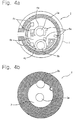
- a condenser microphone 1 includes a case 18, a back pole plate ring 19, a diaphragm 20, a spacer 21, a back pole plate 22, a metal ring 23, a base ring 24, a printed circuit board 2 and an FET 5.
- a sound wave inlet hole through which the sound wave passes is drilled in the upper part of the case 18 made of conductive material.
- the lower end is open so that other elements can be inserted at the manufacturing process, and is folded inward after completing the manufacturing to fix the inserted elements.
- the case 18 electrically connects the back pole plate ring 19 to the pattern formed on the lower surface of the printed circuit board 2.
- a doughnut-shaped back pole plate ring 19 made of conductive material is inserted in the upper end of the interior of the case 18, and a round-shaped diaphragm 20 which vibrates by the sound wave is attached to the bottom surface of the back pole plate ring 19. That is, the diaphragm 20 vibrates by the sound wave and varies the capacitance, thus causing the potential difference at the back pole plate 22 where a plurality of through holes are drilled in.
- a spacer 21 for insulating the diaphragm 20 from the back pole plate 22 is disposed there-between, and a metal ring 23 is inserted in the bottom surface of the spacer 21 to electrically connect the back pole plate 22 to the pattern formed on the upper surface of the printed circuit board 10, i.e., to the gate of the FET 5.
- a base ring 24 made of insulating material is inserted in the outer ring of the metal ring 23 to prevent the back pole plate 22 or the metal ring 23 from being electrically connected to the case 18.
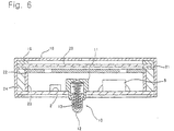
- the printed circuit board 2 having the FET 5 and the connection pin 10 is inserted into the case 18 and then the lower end of the case is folded inward to fix the elements.
- connection patterns 6a, 6b and 6c which are electrically connected to the metal ring 23, the connection pin 10 and each terminal of the FET 5 are formed on the upper surface of the substrate 7 which has a predetermined thickness and is made of insulating material, and a connection pattern which is electrically connected to the source of the FET 5 and the case 18 is formed on the lower surface of the substrate 7.
- a plurality of through holes 3a and 3b are drilled in the substrate 7 to make a plurality of connection pins 10 having a buffering function be inserted and fixed thereto.
- fixing patterns 4a and 4b which are electrically connected to the connection pins 10 by fixing the connection pins 10 are formed around the through holes 3a and 3b.
- connection pins 10 which are inserted and fixed to the through holes 3a and 3b are connected to the source and drain of the FET 5, respectively.
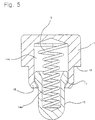
- FIG. 5 is a sectional view showing the connection pins 10 which are inserted and fixed to the through holes 3a and 3b of the printed circuit board 2.
- the connection pin 10 is comprised of a fixed element 11, a movable element 12 and a spring 13.
- the fixed element 11 has an internal space 14a which is opened in one direction, and a folded end part 16 which is folded inward after assembling the movable element 12 and the spring 13 in the internal space 14a is formed at the opened end of the internal space 14a.
- a fixed jaw 15 which is connected to the fixing patterns 4a, 4b of the printed circuit board 2 when inserting and fixing the connection pins 10 to the through holes 3a, 3b of the printed circuit board 2 is horizontally formed at the circumference of the fixed element 11.
- the movable element 12 having a clamping projection 17 which is inserted and combined to the internal space 14a of the fixed element 11 also has an internal space 14b, and the spring 13 is inserted into the internal spaces 14a, 14b between the fixed and movable elements 11, 12 which are assembled to be one connection pin 10, to have the connection pin 10 carry out the buffering function.
- connection pins 10 which have buffering function and are respectively connected to the source and drain of the FET are exposed to the exterior of the condenser microphone 1, it is possible to mount the condenser microphone 1 in the mike, sounding or imaging apparatus and the like without using additional connectors.
- the present invention can reduce connection failure of the condenser microphone without increasing the thickness of the condenser microphone, and can reduce the time required in manufacturing and assembling the condenser microphone.
- the present invention can reduce the thickness of the condenser microphone and mount the condenser microphone on the printed circuit board installed in the mike and the like without using additional connector.
Landscapes
- Physics & Mathematics (AREA)
- Engineering & Computer Science (AREA)
- Acoustics & Sound (AREA)
- Signal Processing (AREA)
- Electrostatic, Electromagnetic, Magneto- Strictive, And Variable-Resistance Transducers (AREA)
- Details Of Audible-Bandwidth Transducers (AREA)
Applications Claiming Priority (2)
| Application Number | Priority Date | Filing Date | Title |
|---|---|---|---|
| KR1019990057017A KR100341564B1 (ko) | 1999-12-13 | 1999-12-13 | 콘덴서 마이크로폰 |
| KR9957017 | 1999-12-13 |
Publications (1)
| Publication Number | Publication Date |
|---|---|
| EP1109422A2 true EP1109422A2 (de) | 2001-06-20 |
Family
ID=19625289
Family Applications (1)
| Application Number | Title | Priority Date | Filing Date |
|---|---|---|---|
| EP00306554A Withdrawn EP1109422A2 (de) | 1999-12-13 | 2000-08-01 | Kondensator-mikrofon |
Country Status (5)
| Country | Link |
|---|---|
| EP (1) | EP1109422A2 (de) |
| JP (1) | JP2001186595A (de) |
| KR (1) | KR100341564B1 (de) |
| CN (1) | CN1305331A (de) |
| TW (1) | TW486917B (de) |
Cited By (5)
| Publication number | Priority date | Publication date | Assignee | Title |
|---|---|---|---|---|
| WO2006135143A1 (en) * | 2005-06-13 | 2006-12-21 | Bse Co., Ltd | Conductive base of condenser microphone and condenser microphone using the same |
| WO2007024047A1 (en) * | 2005-08-20 | 2007-03-01 | Bse Co., Ltd | Electret condenser microphone |
| EP1513370A3 (de) * | 2003-09-08 | 2007-08-15 | Sambu Communics Co., Ltd. | Kondensatormikrofon |
| SG140458A1 (en) * | 2003-07-29 | 2008-03-28 | Bse Co Ltd | Integrated base and electret condenser microphone using the same |
| SG142141A1 (en) * | 2003-11-05 | 2008-05-28 | Bse Co Ltd | Method of mounting condenser microphone on main pcb and condenser microphone adapted for the same |
Families Citing this family (12)
| Publication number | Priority date | Publication date | Assignee | Title |
|---|---|---|---|---|
| JP2001309487A (ja) * | 2000-04-24 | 2001-11-02 | Citizen Electronics Co Ltd | 動電型スピーカ |
| JP4251515B2 (ja) * | 2000-04-24 | 2009-04-08 | シチズン電子株式会社 | 電磁型発音体 |
| KR20020004056A (ko) * | 2000-06-30 | 2002-01-16 | 김종곤 | 이동통신 단말기의 마이크로폰 접속방법 및 그 접속구조 |
| KR20030006116A (ko) * | 2001-07-11 | 2003-01-23 | 엘지전자 주식회사 | 이동통신 단말기의 수화부 통전장치 |
| KR100466403B1 (ko) * | 2002-03-08 | 2005-01-13 | 주식회사 삼부커뮤닉스 | 제품과의 접속을 위한 콘덴서 마이크로폰의 구조 |
| KR100523029B1 (ko) * | 2002-06-14 | 2005-10-24 | 주식회사 씨에스티 | 단일 지향성 초박/초소형 콘덴서 마이크로폰 조립체 및 이에 조립된 단일형 위상지연체 |
| KR100470694B1 (ko) * | 2002-07-24 | 2005-03-10 | (주)제이엠씨 | 휴대폰용 마이크 접속핀 |
| KR100544281B1 (ko) * | 2004-02-24 | 2006-01-23 | 주식회사 비에스이 | 평행육면체형 지향성 콘덴서 마이크로폰 |
| JP4753887B2 (ja) * | 2006-04-07 | 2011-08-24 | 株式会社オーディオテクニカ | マイクロホンのコネクタおよびそのシールド方法 |
| EP2037698B1 (de) * | 2006-07-04 | 2014-09-10 | JVC KENWOOD Corporation | Mikrofonvorrichtung |
| KR100757703B1 (ko) | 2007-03-08 | 2007-09-13 | 주식회사 영은전자 | 판형 커넥터클램프와 이의 내장 인쇄회로기판 및 그제조방법 |
| JP4799577B2 (ja) * | 2008-03-13 | 2011-10-26 | 株式会社オーディオテクニカ | コンデンサーマイクロホン |
Family Cites Families (3)
| Publication number | Priority date | Publication date | Assignee | Title |
|---|---|---|---|---|
| JPH02149198A (ja) * | 1988-11-30 | 1990-06-07 | Matsushita Electric Ind Co Ltd | エレクトレットコンデンサマイクロホン |
| KR19980015053U (ko) * | 1996-09-05 | 1998-06-25 | 문정환 | 반도체 디바이스 테스트용 접속핀 |
| KR200218410Y1 (ko) * | 1998-12-31 | 2001-04-02 | 오 세 옥 | 이동통신 단말기용 콘덴서 마이크로폰 |
-
1999
- 1999-12-13 KR KR1019990057017A patent/KR100341564B1/ko not_active Expired - Fee Related
-
2000
- 2000-07-25 JP JP2000223626A patent/JP2001186595A/ja active Pending
- 2000-07-26 TW TW089114891A patent/TW486917B/zh active
- 2000-07-28 CN CN00121165A patent/CN1305331A/zh active Pending
- 2000-08-01 EP EP00306554A patent/EP1109422A2/de not_active Withdrawn
Cited By (5)
| Publication number | Priority date | Publication date | Assignee | Title |
|---|---|---|---|---|
| SG140458A1 (en) * | 2003-07-29 | 2008-03-28 | Bse Co Ltd | Integrated base and electret condenser microphone using the same |
| EP1513370A3 (de) * | 2003-09-08 | 2007-08-15 | Sambu Communics Co., Ltd. | Kondensatormikrofon |
| SG142141A1 (en) * | 2003-11-05 | 2008-05-28 | Bse Co Ltd | Method of mounting condenser microphone on main pcb and condenser microphone adapted for the same |
| WO2006135143A1 (en) * | 2005-06-13 | 2006-12-21 | Bse Co., Ltd | Conductive base of condenser microphone and condenser microphone using the same |
| WO2007024047A1 (en) * | 2005-08-20 | 2007-03-01 | Bse Co., Ltd | Electret condenser microphone |
Also Published As
| Publication number | Publication date |
|---|---|
| TW486917B (en) | 2002-05-11 |
| CN1305331A (zh) | 2001-07-25 |
| KR20000012565A (ko) | 2000-03-06 |
| JP2001186595A (ja) | 2001-07-06 |
| KR100341564B1 (ko) | 2002-06-22 |
Similar Documents
| Publication | Publication Date | Title |
|---|---|---|
| EP1109422A2 (de) | Kondensator-mikrofon | |
| EP2352311B1 (de) | Mikrofon | |
| JP5216717B2 (ja) | 小型シリコンコンデンサマイクロフォンおよびその製造方法 | |
| US8050443B2 (en) | Microphone and microphone mounting structure | |
| US20070058826A1 (en) | Condenser microphone | |
| JP2003179323A (ja) | 電子回路ユニットの取付構造 | |
| JP2003153392A (ja) | エレクトレットコンデンサマイクロホン | |
| JP2971018B2 (ja) | 電気音響変換器 | |
| US7344405B2 (en) | Electro-acoustic transducer with holder | |
| JP3456042B2 (ja) | 電気音響変換体 | |
| KR100331020B1 (ko) | 플렉시블 기판의 단자 구조 | |
| JP2000277219A (ja) | ローパスフィルタ機能を有するコネクタ | |
| KR100644991B1 (ko) | 표면실장형 일렉트렛 콘덴서 마이크로폰 및 그 제조방법 | |
| JP2003051562A (ja) | 半導体装置 | |
| KR100466403B1 (ko) | 제품과의 접속을 위한 콘덴서 마이크로폰의 구조 | |
| JP2003037884A (ja) | マイクロホンホルダ | |
| JP2002111168A (ja) | リード線を有する電子部品 | |
| JPS5813677Y2 (ja) | 静電型マイクロホン | |
| JP2006060373A (ja) | コンデンサマイクロホン | |
| JP4201298B2 (ja) | 電磁型発音体 | |
| JP2007081844A (ja) | コンデンサマイクロホン、コンデンサマイクロホンの実装方法およびこれを用いた携帯端末 | |
| KR20050045214A (ko) | 지향성 콘덴서 마이크로폰용 홀더 | |
| JPH1065567A (ja) | 無線通信装置 | |
| JPS63280489A (ja) | 複合プリント基板 | |
| JP2004038266A (ja) | カード装置 |
Legal Events
| Date | Code | Title | Description |
|---|---|---|---|
| PUAI | Public reference made under article 153(3) epc to a published international application that has entered the european phase |
Free format text: ORIGINAL CODE: 0009012 |
|
| AK | Designated contracting states |
Kind code of ref document: A2 Designated state(s): AT BE CH CY DE DK ES FI FR GB GR IE IT LI LU MC NL PT SE |
|
| AX | Request for extension of the european patent |
Free format text: AL;LT;LV;MK;RO;SI |
|
| STAA | Information on the status of an ep patent application or granted ep patent |
Free format text: STATUS: THE APPLICATION IS DEEMED TO BE WITHDRAWN |
|
| 18D | Application deemed to be withdrawn |
Effective date: 20030418 |