EP1109422A2 - Condenser microphone - Google Patents
Condenser microphone Download PDFInfo
- Publication number
- EP1109422A2 EP1109422A2 EP00306554A EP00306554A EP1109422A2 EP 1109422 A2 EP1109422 A2 EP 1109422A2 EP 00306554 A EP00306554 A EP 00306554A EP 00306554 A EP00306554 A EP 00306554A EP 1109422 A2 EP1109422 A2 EP 1109422A2
- Authority
- EP
- European Patent Office
- Prior art keywords
- condenser microphone
- fet
- circuit board
- printed circuit
- holes
- Prior art date
- Legal status (The legal status is an assumption and is not a legal conclusion. Google has not performed a legal analysis and makes no representation as to the accuracy of the status listed.)
- Withdrawn
Links
Images


Classifications
-
- H—ELECTRICITY
- H04—ELECTRIC COMMUNICATION TECHNIQUE
- H04R—LOUDSPEAKERS, MICROPHONES, GRAMOPHONE PICK-UPS OR LIKE ACOUSTIC ELECTROMECHANICAL TRANSDUCERS; DEAF-AID SETS; PUBLIC ADDRESS SYSTEMS
- H04R19/00—Electrostatic transducers
-
- H—ELECTRICITY
- H04—ELECTRIC COMMUNICATION TECHNIQUE
- H04R—LOUDSPEAKERS, MICROPHONES, GRAMOPHONE PICK-UPS OR LIKE ACOUSTIC ELECTROMECHANICAL TRANSDUCERS; DEAF-AID SETS; PUBLIC ADDRESS SYSTEMS
- H04R1/00—Details of transducers, loudspeakers or microphones
- H04R1/06—Arranging circuit leads; Relieving strain on circuit leads
-
- H—ELECTRICITY
- H04—ELECTRIC COMMUNICATION TECHNIQUE
- H04R—LOUDSPEAKERS, MICROPHONES, GRAMOPHONE PICK-UPS OR LIKE ACOUSTIC ELECTROMECHANICAL TRANSDUCERS; DEAF-AID SETS; PUBLIC ADDRESS SYSTEMS
- H04R19/00—Electrostatic transducers
- H04R19/04—Microphones
Definitions
- the present invention relates to a condenser microphone, and more particularly to a condenser microphone wherein a connector for connecting each terminal of the condenser microphone to an external line is integrated in the condenser microphone, thus enabling the reduction of the thickness of the condenser microphone and the simplification of assembling process.
- Known condenser microphones can be divided into a pin type condenser microphone and an SMD (Surface Mounting Device) type condenser microphone.
- SMD Surface Mounting Device
- the SMD type condenser microphone has a plane bottom surface, and thus it can be easily fixed to a printed circuit board by using a cream solder.
- a case of the condenser microphone 101, 111 is folded with enclosing the printed circuit board as shown in figs. 1 and 2, the case has a different height from that of the printed circuit board.
- the pattern formed on the printed circuit board may not be correctly connected when soldering or depositing the condenser microphone 101, 111 to the printed circuit board.
- a connector 102, 112 having a terminal 103, 113 for connecting the pattern of the condenser microphone 101, 111 to an exterior is additionally provided, as shown in figs. 1 and 2, thus preventing the malfunction of the condenser microphone due to connection failure.
- a primary object of the present invention is to at least partly mitigate disadvantages of the prior art.
- Embodiments of the present invention provide a condenser microphone which can reduce connection failure of the condenser microphone without increasing the thickness thereof, and can reduce the time required in manufacturing and assembling the condenser microphone.
- the condenser microphone of the present invention includes a case whose upper surface has a sound wave inlet hole drilled in and the lower surface is opened; a back pole plate ring which is inserted in the case and electrically connected to the source of a FET via the case; a diaphragm which is attached to the lower surface of the back pole plate ring and is vibrated by the sound wave passing through the sound wave inlet hole; a spacer which insulates the diaphragm from a back pole plate; the back pole plate which has a plurality of through holes, converts the variation of the capacitance caused by the vibration of the diaphragm into a potential difference and applies it to the gate of the FET via a metal ring; the metal ring which has a base ring placed at the circumference thereof and electrically connects the back pole plate to the gate of the FET; a printed circuit board whose patterns to be electrically connected to each terminal of the FET, the metal ring and the case are formed at both sides
- the printed circuit board has a substrate which has a predetermined thickness and is made of insulating material; a first connection pattern which is formed on the upper surface of the substrate to be electrically connected to the metal ring, the connection pins and each terminal of the FET; a second connection pattern which is formed on the lower surface of the substrate to be electrically connected to the source of the FET and the case; and a plurality of through holes which pass through the substrate up and down.
- connection pin has a fixed element which has an internal space opened in one direction and a folded end part formed at the end of the opened space to be folded inward; a movable element which has an internal space opened in one direction and a clamping projection formed at the circumference of the end of the opened space; and a spring which is inserted in the internal space between the fixed element and the movable element.
- the fixed element, the movable element and the spring are plated with gold. Also, it is preferable that a fixed jaw connected to the pattern formed at the circumference of the through holes is horizontally formed at the circumference of the fixed element.
- a condenser microphone 1 includes a case 18, a back pole plate ring 19, a diaphragm 20, a spacer 21, a back pole plate 22, a metal ring 23, a base ring 24, a printed circuit board 2 and an FET 5.
- a sound wave inlet hole through which the sound wave passes is drilled in the upper part of the case 18 made of conductive material.
- the lower end is open so that other elements can be inserted at the manufacturing process, and is folded inward after completing the manufacturing to fix the inserted elements.
- the case 18 electrically connects the back pole plate ring 19 to the pattern formed on the lower surface of the printed circuit board 2.
- a doughnut-shaped back pole plate ring 19 made of conductive material is inserted in the upper end of the interior of the case 18, and a round-shaped diaphragm 20 which vibrates by the sound wave is attached to the bottom surface of the back pole plate ring 19. That is, the diaphragm 20 vibrates by the sound wave and varies the capacitance, thus causing the potential difference at the back pole plate 22 where a plurality of through holes are drilled in.
- a spacer 21 for insulating the diaphragm 20 from the back pole plate 22 is disposed there-between, and a metal ring 23 is inserted in the bottom surface of the spacer 21 to electrically connect the back pole plate 22 to the pattern formed on the upper surface of the printed circuit board 10, i.e., to the gate of the FET 5.
- a base ring 24 made of insulating material is inserted in the outer ring of the metal ring 23 to prevent the back pole plate 22 or the metal ring 23 from being electrically connected to the case 18.
- the printed circuit board 2 having the FET 5 and the connection pin 10 is inserted into the case 18 and then the lower end of the case is folded inward to fix the elements.
- connection patterns 6a, 6b and 6c which are electrically connected to the metal ring 23, the connection pin 10 and each terminal of the FET 5 are formed on the upper surface of the substrate 7 which has a predetermined thickness and is made of insulating material, and a connection pattern which is electrically connected to the source of the FET 5 and the case 18 is formed on the lower surface of the substrate 7.
- a plurality of through holes 3a and 3b are drilled in the substrate 7 to make a plurality of connection pins 10 having a buffering function be inserted and fixed thereto.
- fixing patterns 4a and 4b which are electrically connected to the connection pins 10 by fixing the connection pins 10 are formed around the through holes 3a and 3b.
- connection pins 10 which are inserted and fixed to the through holes 3a and 3b are connected to the source and drain of the FET 5, respectively.
- FIG. 5 is a sectional view showing the connection pins 10 which are inserted and fixed to the through holes 3a and 3b of the printed circuit board 2.
- the connection pin 10 is comprised of a fixed element 11, a movable element 12 and a spring 13.
- the fixed element 11 has an internal space 14a which is opened in one direction, and a folded end part 16 which is folded inward after assembling the movable element 12 and the spring 13 in the internal space 14a is formed at the opened end of the internal space 14a.
- a fixed jaw 15 which is connected to the fixing patterns 4a, 4b of the printed circuit board 2 when inserting and fixing the connection pins 10 to the through holes 3a, 3b of the printed circuit board 2 is horizontally formed at the circumference of the fixed element 11.
- the movable element 12 having a clamping projection 17 which is inserted and combined to the internal space 14a of the fixed element 11 also has an internal space 14b, and the spring 13 is inserted into the internal spaces 14a, 14b between the fixed and movable elements 11, 12 which are assembled to be one connection pin 10, to have the connection pin 10 carry out the buffering function.
- connection pins 10 which have buffering function and are respectively connected to the source and drain of the FET are exposed to the exterior of the condenser microphone 1, it is possible to mount the condenser microphone 1 in the mike, sounding or imaging apparatus and the like without using additional connectors.
- the present invention can reduce connection failure of the condenser microphone without increasing the thickness of the condenser microphone, and can reduce the time required in manufacturing and assembling the condenser microphone.
- the present invention can reduce the thickness of the condenser microphone and mount the condenser microphone on the printed circuit board installed in the mike and the like without using additional connector.
Abstract
In the present invention, two through holes are drilled in the printed circuit board, the
connection pins are respectively inserted to the through holes with one end being exposed to
the exterior and then each connection pin is connected to the drain and source of the FET.
Accordingly, the present invention can reduce the thickness of the condenser microphone and
mount the condenser microphone on the printed circuit board installed in the microphone and
the like without using additional connector.
Description
- The present invention relates to a condenser microphone, and more particularly to a condenser microphone wherein a connector for connecting each terminal of the condenser microphone to an external line is integrated in the condenser microphone, thus enabling the reduction of the thickness of the condenser microphone and the simplification of assembling process.
- Known condenser microphones can be divided into a pin type condenser microphone and an SMD (Surface Mounting Device) type condenser microphone.
- The SMD type condenser microphone has a plane bottom surface, and thus it can be easily fixed to a printed circuit board by using a cream solder. In addition, since a case of the
condenser microphone - Thereby, the pattern formed on the printed circuit board may not be correctly connected when soldering or depositing the
condenser microphone - Hence, in a prior art, a
connector terminal condenser microphone - In this case, however, not only economical/time losses are incurred due to the additional connectors but the total thickness of the condenser microphone is increased because of the added thickness the connectors. Also, the working time for placing the condenser microphone having the connectors is increased.
- A primary object of the present invention is to at least partly mitigate disadvantages of the prior art.
- Embodiments of the present invention provide a condenser microphone which can reduce connection failure of the condenser microphone without increasing the thickness thereof, and can reduce the time required in manufacturing and assembling the condenser microphone.
- To achieve the above object, the condenser microphone of the present invention includes a case whose upper surface has a sound wave inlet hole drilled in and the lower surface is opened; a back pole plate ring which is inserted in the case and electrically connected to the source of a FET via the case; a diaphragm which is attached to the lower surface of the back pole plate ring and is vibrated by the sound wave passing through the sound wave inlet hole; a spacer which insulates the diaphragm from a back pole plate; the back pole plate which has a plurality of through holes, converts the variation of the capacitance caused by the vibration of the diaphragm into a potential difference and applies it to the gate of the FET via a metal ring; the metal ring which has a base ring placed at the circumference thereof and electrically connects the back pole plate to the gate of the FET; a printed circuit board whose patterns to be electrically connected to each terminal of the FET, the metal ring and the case are formed at both sides thereof, and a plurality of through holes wherein connection pins to be inserted are drilled in; and the connection pins which are inserted in the through holes of the printed circuit board with the end thereof being exposed to the exterior and has a buffering function.
- Advantageously, the printed circuit board has a substrate which has a predetermined thickness and is made of insulating material; a first connection pattern which is formed on the upper surface of the substrate to be electrically connected to the metal ring, the connection pins and each terminal of the FET; a second connection pattern which is formed on the lower surface of the substrate to be electrically connected to the source of the FET and the case; and a plurality of through holes which pass through the substrate up and down.
- Conveniently, the connection pin has a fixed element which has an internal space opened in one direction and a folded end part formed at the end of the opened space to be folded inward; a movable element which has an internal space opened in one direction and a clamping projection formed at the circumference of the end of the opened space; and a spring which is inserted in the internal space between the fixed element and the movable element.
- Here, it is preferable that the fixed element, the movable element and the spring are plated with gold. Also, it is preferable that a fixed jaw connected to the pattern formed at the circumference of the through holes is horizontally formed at the circumference of the fixed element.
- A preferred embodiment of the present invention will be described, by way of example only, in detail with reference to the accompanying drawings, in which:
- FIG. 1 is a partially cut away separated perspective view showing an example of a conventional condenser microphone and connector combined thereto;
- FIG. 2 is a partially cutaway separated perspective view of showing another example of a conventional condenser microphone and a connector combined thereto;
- FIG. 3 is a partially cutaway separated perspective view of showing an embodiment of a condenser microphone and connection pins combined thereto according to the present invention;
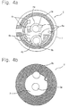
- FIG. 4a is a plan view showing a printed circuit board applied to the condenser microphone according to the present invention;
- FIG. 4b is a front view showing the printed circuit board applied to the condenser microphone according to the present invention;
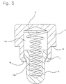
- FIG. 5 is a sectional view showing the connection pin applied to the condenser microphone according to the present invention; and
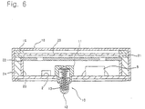
- FIG. 6 is a sectional view showing the combining state of the condenser microphone and connection pin according to the present invention.
-
- In the various figures, like reference numerals refer to like parts.
- As shown in FIG. 3, a condenser microphone 1 includes a
case 18, a backpole plate ring 19, adiaphragm 20, aspacer 21, aback pole plate 22, ametal ring 23, abase ring 24, a printedcircuit board 2 and an FET 5. - A sound wave inlet hole through which the sound wave passes is drilled in the upper part of the
case 18 made of conductive material. The lower end is open so that other elements can be inserted at the manufacturing process, and is folded inward after completing the manufacturing to fix the inserted elements. Thecase 18 electrically connects the backpole plate ring 19 to the pattern formed on the lower surface of the printedcircuit board 2. - A doughnut-shaped back
pole plate ring 19 made of conductive material is inserted in the upper end of the interior of thecase 18, and a round-shaped diaphragm 20 which vibrates by the sound wave is attached to the bottom surface of the backpole plate ring 19. That is, thediaphragm 20 vibrates by the sound wave and varies the capacitance, thus causing the potential difference at theback pole plate 22 where a plurality of through holes are drilled in. - A
spacer 21 for insulating thediaphragm 20 from theback pole plate 22 is disposed there-between, and ametal ring 23 is inserted in the bottom surface of thespacer 21 to electrically connect theback pole plate 22 to the pattern formed on the upper surface of the printedcircuit board 10, i.e., to the gate of theFET 5. - In this case, a
base ring 24 made of insulating material is inserted in the outer ring of themetal ring 23 to prevent theback pole plate 22 or themetal ring 23 from being electrically connected to thecase 18. - Lastly, the printed
circuit board 2 having theFET 5 and theconnection pin 10 is inserted into thecase 18 and then the lower end of the case is folded inward to fix the elements. - Regarding the printed
circuit board 2, as shown in figs. 4a and 4b,connection patterns 6a, 6b and 6c which are electrically connected to themetal ring 23, theconnection pin 10 and each terminal of theFET 5 are formed on the upper surface of thesubstrate 7 which has a predetermined thickness and is made of insulating material, and a connection pattern which is electrically connected to the source of theFET 5 and thecase 18 is formed on the lower surface of thesubstrate 7. A plurality of throughholes substrate 7 to make a plurality ofconnection pins 10 having a buffering function be inserted and fixed thereto. Particularly,fixing patterns connection pins 10 by fixing theconnection pins 10 are formed around the throughholes - Here, the
connection pins 10 which are inserted and fixed to the throughholes FET 5, respectively. - FIG. 5 is a sectional view showing the
connection pins 10 which are inserted and fixed to the throughholes circuit board 2. Here, theconnection pin 10 is comprised of afixed element 11, amovable element 12 and aspring 13. - The
fixed element 11 has aninternal space 14a which is opened in one direction, and a foldedend part 16 which is folded inward after assembling themovable element 12 and thespring 13 in theinternal space 14a is formed at the opened end of theinternal space 14a. In addition, afixed jaw 15 which is connected to thefixing patterns circuit board 2 when inserting and fixing theconnection pins 10 to the throughholes circuit board 2 is horizontally formed at the circumference of thefixed element 11. - The
movable element 12 having aclamping projection 17 which is inserted and combined to theinternal space 14a of thefixed element 11 also has an internal space 14b, and thespring 13 is inserted into theinternal spaces 14a, 14b between the fixed andmovable elements connection pin 10, to have theconnection pin 10 carry out the buffering function. - By gold plating the
fixed element 11, themovable element 12 and thespring 13, it is possible to enhance the electric characteristics. - Since the
connection pins 10 which have buffering function and are respectively connected to the source and drain of the FET are exposed to the exterior of the condenser microphone 1, it is possible to mount the condenser microphone 1 in the mike, sounding or imaging apparatus and the like without using additional connectors. - Accordingly, the present invention can reduce connection failure of the condenser microphone without increasing the thickness of the condenser microphone, and can reduce the time required in manufacturing and assembling the condenser microphone.
- That is, the present invention can reduce the thickness of the condenser microphone and mount the condenser microphone on the printed circuit board installed in the mike and the like without using additional connector.
- Although the present invention has been described in accordance with the embodiment shown in the figures, various modifications and changes may be made by one of ordinary skill in the art without departing from the scope of the present invention which is defined by the appended claims.
Claims (5)
- A condenser microphone comprising:a case having an upper surface, said upper surface having a sound wave inlet hole therein and a lower surface opened;a back pole plate ring inserted into said case and electrically connected to a source of a FET via said case;a diaphragm which is attached to a lower surface of said back pole plate ring and is, in use, vibrated by the sound wave passing though said sound wave inlet hole;a spacer which insulates said diaphragm from a back pole plate;said back pole plate which has a plurality of through holes, converts the variation of the capacitance caused by the vibration of said diaphragm into a potential difference and applies it to a gate of said FET via a metal ring;said metal ring which has a base ring placed at the circumference thereof and electrically connects said back pole plate to a gate of said FET;a printed circuit board whose patterns to be electrically connected to each terminal of said FET, said metal ring and said case are formed at both sides of said printed circuit board and a plurality of through holes wherein connection pins to be inserted and fixed are drilled in; andsaid connection pins which are inserted and fixed to said through holes of said printed circuit board with the end thereof being exposed to an exterior whereby said pins have a buffering function.
- The condenser microphone as claimed in claim 1, wherein said printed circuit board comprises a substrate which has a predetermined thickness and is made of insulating material;a first connection pattern which is formed on the upper surface of said substrate to be electrically connected to said metal ring, said connection pins and each terminal of said FET;a second connection pattern which is formed on the lower surface of said substrate to be electrically connected to a source of said FET and said case; anda plurality of through holes which pass through said substrate up and down.
- The condenser microphone as claimed in claim 1 or 2, wherein said connection pin comprises a fixed element which has an internal space opened in one direction and a folded end part formed at the end of the opened space to be folded inward; a movable element which has an internal space opened in one direction and a clamping projection formed at the circumference of the end of the opened space; and a spring which is disposed in the internal space between said fixed element and said movable element.
- The condenser microphone as claimed in claim 3, wherein said fixed element, said movable element and said spring are plated with gold.
- The condenser microphone as claimed in claim 3 or 4, wherein a fixed jaw connected to the pattern formed at the circumference of said through holes is horizontally disposed at the circumference of said fixed element.
Applications Claiming Priority (2)
| Application Number | Priority Date | Filing Date | Title |
|---|---|---|---|
| KR9957017 | 1999-12-13 | ||
| KR1019990057017A KR100341564B1 (en) | 1999-12-13 | 1999-12-13 | Condenser microphone |
Publications (1)
| Publication Number | Publication Date |
|---|---|
| EP1109422A2 true EP1109422A2 (en) | 2001-06-20 |
Family
ID=19625289
Family Applications (1)
| Application Number | Title | Priority Date | Filing Date |
|---|---|---|---|
| EP00306554A Withdrawn EP1109422A2 (en) | 1999-12-13 | 2000-08-01 | Condenser microphone |
Country Status (5)
| Country | Link |
|---|---|
| EP (1) | EP1109422A2 (en) |
| JP (1) | JP2001186595A (en) |
| KR (1) | KR100341564B1 (en) |
| CN (1) | CN1305331A (en) |
| TW (1) | TW486917B (en) |
Cited By (5)
| Publication number | Priority date | Publication date | Assignee | Title |
|---|---|---|---|---|
| EP1513370A2 (en) * | 2003-09-08 | 2005-03-09 | Sambu Communics Co., Ltd. | Condenser microphone |
| WO2006135143A1 (en) * | 2005-06-13 | 2006-12-21 | Bse Co., Ltd | Conductive base of condenser microphone and condenser microphone using the same |
| WO2007024047A1 (en) * | 2005-08-20 | 2007-03-01 | Bse Co., Ltd | Electret condenser microphone |
| SG140458A1 (en) * | 2003-07-29 | 2008-03-28 | Bse Co Ltd | Integrated base and electret condenser microphone using the same |
| SG142141A1 (en) * | 2003-11-05 | 2008-05-28 | Bse Co Ltd | Method of mounting condenser microphone on main pcb and condenser microphone adapted for the same |
Families Citing this family (12)
| Publication number | Priority date | Publication date | Assignee | Title |
|---|---|---|---|---|
| JP2001309487A (en) * | 2000-04-24 | 2001-11-02 | Citizen Electronics Co Ltd | Electrodynamic loudspeaker |
| JP4251515B2 (en) * | 2000-04-24 | 2009-04-08 | シチズン電子株式会社 | Electromagnetic sound generator |
| KR20020004056A (en) * | 2000-06-30 | 2002-01-16 | 김종곤 | Connection method for microphone of mobile radio communication unit and structure thereof |
| KR20030006116A (en) * | 2001-07-11 | 2003-01-23 | 엘지전자 주식회사 | Electricity transmitter for a receiver module of mobile phone |
| KR100466403B1 (en) * | 2002-03-08 | 2005-01-13 | 주식회사 삼부커뮤닉스 | Condenser microphone |
| KR100523029B1 (en) * | 2002-06-14 | 2005-10-24 | 주식회사 씨에스티 | Ultra-small-size/ultra-thin type cardioid condenser microphone assembly and singleness type phase delay device assembled the same |
| KR100470694B1 (en) * | 2002-07-24 | 2005-03-10 | (주)제이엠씨 | connection pin for cellular phone mike |
| KR100544281B1 (en) * | 2004-02-24 | 2006-01-23 | 주식회사 비에스이 | A parallelepiped type directional condenser microphone |
| JP4753887B2 (en) * | 2006-04-07 | 2011-08-24 | 株式会社オーディオテクニカ | Microphone connector and shielding method thereof |
| JP4565035B2 (en) * | 2006-07-04 | 2010-10-20 | 日本ビクター株式会社 | Microphone device |
| KR100757703B1 (en) | 2007-03-08 | 2007-09-13 | 주식회사 영은전자 | A panel type connector clamp and a pcb(printed circuit board) including that and its manufacturing method |
| JP4799577B2 (en) * | 2008-03-13 | 2011-10-26 | 株式会社オーディオテクニカ | Condenser microphone |
Family Cites Families (3)
| Publication number | Priority date | Publication date | Assignee | Title |
|---|---|---|---|---|
| JPH02149198A (en) * | 1988-11-30 | 1990-06-07 | Matsushita Electric Ind Co Ltd | Electlet condenser microphone |
| KR19980015053U (en) * | 1996-09-05 | 1998-06-25 | 문정환 | Connection pin for semiconductor device test |
| KR200218410Y1 (en) * | 1998-12-31 | 2001-04-02 | 오 세 옥 | Condenser microphone for mobile terminal |
-
1999
- 1999-12-13 KR KR1019990057017A patent/KR100341564B1/en not_active IP Right Cessation
-
2000
- 2000-07-25 JP JP2000223626A patent/JP2001186595A/en active Pending
- 2000-07-26 TW TW089114891A patent/TW486917B/en active
- 2000-07-28 CN CN00121165A patent/CN1305331A/en active Pending
- 2000-08-01 EP EP00306554A patent/EP1109422A2/en not_active Withdrawn
Cited By (6)
| Publication number | Priority date | Publication date | Assignee | Title |
|---|---|---|---|---|
| SG140458A1 (en) * | 2003-07-29 | 2008-03-28 | Bse Co Ltd | Integrated base and electret condenser microphone using the same |
| EP1513370A2 (en) * | 2003-09-08 | 2005-03-09 | Sambu Communics Co., Ltd. | Condenser microphone |
| EP1513370A3 (en) * | 2003-09-08 | 2007-08-15 | Sambu Communics Co., Ltd. | Condenser microphone |
| SG142141A1 (en) * | 2003-11-05 | 2008-05-28 | Bse Co Ltd | Method of mounting condenser microphone on main pcb and condenser microphone adapted for the same |
| WO2006135143A1 (en) * | 2005-06-13 | 2006-12-21 | Bse Co., Ltd | Conductive base of condenser microphone and condenser microphone using the same |
| WO2007024047A1 (en) * | 2005-08-20 | 2007-03-01 | Bse Co., Ltd | Electret condenser microphone |
Also Published As
| Publication number | Publication date |
|---|---|
| TW486917B (en) | 2002-05-11 |
| KR20000012565A (en) | 2000-03-06 |
| CN1305331A (en) | 2001-07-25 |
| JP2001186595A (en) | 2001-07-06 |
| KR100341564B1 (en) | 2002-06-22 |
Similar Documents
| Publication | Publication Date | Title |
|---|---|---|
| EP1109422A2 (en) | Condenser microphone | |
| EP2352311B1 (en) | Microphone | |
| JP5216717B2 (en) | Small silicon condenser microphone and manufacturing method thereof | |
| US8050443B2 (en) | Microphone and microphone mounting structure | |
| US20070058826A1 (en) | Condenser microphone | |
| JP2003179323A (en) | Attaching structure for electronic circuit unit | |
| KR100675027B1 (en) | Silicon based condenser microphone and mounting method for the same | |
| JP2003153392A (en) | Electret capacitor microphone | |
| US7344405B2 (en) | Electro-acoustic transducer with holder | |
| JP2971018B2 (en) | Electroacoustic transducer | |
| KR100644991B1 (en) | Surface mounting type electret condenser microphone and method of manufacturing the same | |
| JP3456042B2 (en) | Electroacoustic transducer | |
| EP1107642A2 (en) | Condenser microphone | |
| JP2003051562A (en) | Semiconductor device | |
| JP2007081844A (en) | Condenser microphone, mounting method of condenser microphone and portable terminal using the same | |
| KR100331020B1 (en) | terminal of flexible printed circuit and method there of | |
| KR100466403B1 (en) | Condenser microphone | |
| JP2000277219A (en) | Connector having low-pass filter function | |
| JP2006060373A (en) | Condenser microphone | |
| JP2002111168A (en) | Electronic part with lead wire | |
| JPS5813677Y2 (en) | electrostatic microphone | |
| JP4201298B2 (en) | Electromagnetic sound generator | |
| KR20050045214A (en) | Holder for directional condenser microphone | |
| JP2003037884A (en) | Microphone holder | |
| JPS63280489A (en) | Composite printed board |
Legal Events
| Date | Code | Title | Description |
|---|---|---|---|
| PUAI | Public reference made under article 153(3) epc to a published international application that has entered the european phase |
Free format text: ORIGINAL CODE: 0009012 |
|
| AK | Designated contracting states |
Kind code of ref document: A2 Designated state(s): AT BE CH CY DE DK ES FI FR GB GR IE IT LI LU MC NL PT SE |
|
| AX | Request for extension of the european patent |
Free format text: AL;LT;LV;MK;RO;SI |
|
| STAA | Information on the status of an ep patent application or granted ep patent |
Free format text: STATUS: THE APPLICATION IS DEEMED TO BE WITHDRAWN |
|
| 18D | Application deemed to be withdrawn |
Effective date: 20030418 |