EP1109220A2 - Dielektrische Füllung von elektrischen Verdrahtungsebenen - Google Patents
Dielektrische Füllung von elektrischen Verdrahtungsebenen Download PDFInfo
- Publication number
- EP1109220A2 EP1109220A2 EP00126887A EP00126887A EP1109220A2 EP 1109220 A2 EP1109220 A2 EP 1109220A2 EP 00126887 A EP00126887 A EP 00126887A EP 00126887 A EP00126887 A EP 00126887A EP 1109220 A2 EP1109220 A2 EP 1109220A2
- Authority
- EP
- European Patent Office
- Prior art keywords
- layer
- dielectric layer
- electrical wiring
- conductor track
- trench
- Prior art date
- Legal status (The legal status is an assumption and is not a legal conclusion. Google has not performed a legal analysis and makes no representation as to the accuracy of the status listed.)
- Withdrawn
Links
Images
Classifications
-
- H—ELECTRICITY
- H10—SEMICONDUCTOR DEVICES; ELECTRIC SOLID-STATE DEVICES NOT OTHERWISE PROVIDED FOR
- H10P—GENERIC PROCESSES OR APPARATUS FOR THE MANUFACTURE OR TREATMENT OF DEVICES COVERED BY CLASS H10
- H10P14/00—Formation of materials, e.g. in the shape of layers or pillars
- H10P14/40—Formation of materials, e.g. in the shape of layers or pillars of conductive or resistive materials
-
- H—ELECTRICITY
- H10—SEMICONDUCTOR DEVICES; ELECTRIC SOLID-STATE DEVICES NOT OTHERWISE PROVIDED FOR
- H10W—GENERIC PACKAGES, INTERCONNECTIONS, CONNECTORS OR OTHER CONSTRUCTIONAL DETAILS OF DEVICES COVERED BY CLASS H10
- H10W20/00—Interconnections in chips, wafers or substrates
- H10W20/40—Interconnections external to wafers or substrates, e.g. back-end-of-line [BEOL] metallisations or vias connecting to gate electrodes
- H10W20/45—Interconnections external to wafers or substrates, e.g. back-end-of-line [BEOL] metallisations or vias connecting to gate electrodes characterised by their insulating parts
- H10W20/48—Insulating materials thereof
Definitions
- the present invention relates to dielectric filling of electrical wiring levels in one integrated Circuit.
- Integrated circuits consist of a large number of individual structures, mostly arranged in layers on a substrate are.
- Electronic components are usually used such as resistors, capacitors, diodes, transistors etc. in made of a substrate.
- the electrical connection of the individual components then take place in one or more wiring levels above (so-called metallization levels).
- a method used for electrical wiring will see the deposition of a conductive layer on top of one Substrate before.
- the conductive layer is then photolithographically structured so that traces with an intermediate Ditches arise.
- a dielectric made of silicon oxide.
- doped silicon oxides such as borosilicate glass, Phosphorus silicate glass or arsenic silicate glass or mixtures of used these materials.
- the doped silicate glasses have the property of flowing at high temperatures. This enables the trench to be insulated Fill up dielectric.
- the doped silicate glasses have the disadvantage that they have a high dielectric constant of approx. 4.
- the high dielectric constant has an adverse effect the signal propagation speed on the electrical Connection lines made by the high dielectric constant have a large capacity.
- the large capacity leads to great RC times.
- the problem of large RC times is exacerbated themselves in the future because the distances between the individual tracks due to the general trend too always smaller components, continues to decrease, resulting in larger ones Capacities.
- Another problem with the steady downsizing of the electrical circuitry is limited Flowability of the doped silicate glass. This creates with increasingly smaller trenches between the conductor tracks So-called blowholes, into which the doped silicate glass can no longer get into. The blowholes have the unpleasant quality To accumulate moisture. At a temperature step, the the integrated switching circuit e.g. experiences when soldered, explodes the integrated circuit through the evaporation the accumulated moisture and is therefore unusable.
- Another disadvantage is the high reflectivity of the doped silicate glass layers used in subsequent lithographic Steps towards incorrect exposures and incorrect processing leads.
- polybenzoxazole In addition to polybenzoxazole, other materials are suitable, which also by spin on a Wafers can be applied. These include inorganic Materials such as hydrogen silsesquioxane and organic materials such as polybenzoxazoles, polyimides, perylenes, polynorbornenes and polytetrafluoroethylene and their derivatives, such as especially their fluorinated derivatives.
- inorganic Materials such as hydrogen silsesquioxane
- organic materials such as polybenzoxazoles, polyimides, perylenes, polynorbornenes and polytetrafluoroethylene and their derivatives, such as especially their fluorinated derivatives.
- the polymer material polybenzoxazole (PBO) is characterized by this from that by spin coating can be applied and thus the smallest gaps without voids fills. This avoids cavities in a HAST test (Humidity Accelleration Stress Test) Accumulate moisture and explode in subsequent temperature steps can (popcorn effect).
- HAST test Human Industry Accelleration Stress Test
- the dielectric constant of polybenzoxazole in the hardened state less than 2.9. The minor Dielectric constant enables due to the lower parasitic capacitances faster signals on the integrated Circuit.
- polybenzoxazole hampers its absorption properties in subsequent reflections photolithographic exposure steps. This will make one significantly improved resolution in subsequent photolithographic Steps achieved.
- the arrangement according to the invention is a silicon nitride layer above the dielectric layer arranged.
- the silicon nitride layer has the Advantage that they are excellent as a passivation layer Barrier effect against water vapor, alkali ions and other corrosive acting substances can be used.
- Arrangement is made between the first dielectric Layer and the silicon nitride layer a silicon oxide layer arranged.
- Arrangement is above the first dielectric Layer a second dielectric layer made of polybenzoxazole or a photosensitive polyimide.
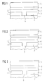
- FIG 1 is a layer structure of an electrical wiring shown according to the prior art.
- Base body 1 which already has electronic components such as Resistors, capacitors, diodes, transistors, passivation layers etc. may include a conductive Layer 2 deposited.
- the conductive one Layer 2 is formed from a metal such as aluminum or copper.
- the conductive layer 2 is structured so that a first conductor track 3 and a second conductor track 4 with an intermediate one Trench 5 arise. Then usually deposited a doped silicate glass and with a Temperature step flowed so that it fills the trench 5 and forms a silicon oxide layer 7.
- silicon oxide layer 7 then becomes a silicon nitride layer 8 formed as a passivation layer with excellent Blocking effect.
- the second dielectric layer 9 serves as photosensitive Layer (photoresist) and consists for example of a polyimide, a photosensitive polyimide, a polyimide derivative, a polybenzoxazole, a photosensitive polybenzoxazole or from a polybenzoxazole derivative.
- first dielectric Layer 6 for filling the trench 5 and for covering the conductive layer 2 and thus to cover the first conductor 3 and the second conductor track 4 is used.
- At the first dielectric layer 6 is, for example around the polymer material polybenzoxazole.
- the invention Advantage of the first dielectric layer 6 polybenzoxazole has excellent filling properties, the low dielectric constant, the smaller than 2.9 and the reduction of reflections in subsequent ones Lithography steps.
- the dielectric layer 6 the silicon nitride layer 8 is formed.
- the dielectric Layer 6 as a stress reduction layer compared to the often mechanical strained silicon nitride layer 8 acts and thereby Integration problems caused by mechanical stress the silicon nitride layer are caused, reduced or eliminated become.
- the layer thickness of the dielectric Layer 6 in Figure 3 are made smaller than the layer thickness of the silicon oxide layer 7 from FIG. 1, whereby subsequent dry etching steps to open the passivation layer shorter and therefore more economical become.
Landscapes
- Internal Circuitry In Semiconductor Integrated Circuit Devices (AREA)
- Formation Of Insulating Films (AREA)
Abstract
Description
- einem Grundkörper;
- einer leitfähigen Schicht, die auf dem Grundkörper angeordnet ist und so strukturiert ist, daß sie eine erste Leiterbahn, eine zweite Leiterbahn und einen Graben zwischen der ersten Leiterbahn und der zweiten Leiterbahn aufweist;
- einer ersten dielektrischen Schicht, die auf der leitfähigen Schicht angeordnet ist und den Graben zumindest teilweise ausfüllt,
- wobei die erste dielektrische Schicht einen der Polymerwerkstoffe Polybenzoxazol und/oder Polynorbornen und/oder eines ihrer Derivate umfaßt.
- Bilden einer leitfähigen Schicht auf einem Grundkörper;
- Strukturieren der leitfähigen Schicht, so daß eine erste Leiterbahn, eine zweite Leiterbahn und ein Graben zwischen der ersten Leiterbahn und der zweiten Leiterbahn gebildet wird,
- wobei eine erste dielektrische Schicht aus einem Polymer auf der leitfähigen Schicht aufgeschleudert wird, so daß der Graben zumindest teilweise aufgefüllt wird, wobei das Polymer Polybenzoxazol und/oder Polynorbornen und/oder eines ihrer Derivate umfaßt.
- Figur 1
- einen Schichtaufbau zur elektrischen Verdrahtung gemäß dem Stand der Technik;
- Figur 2
- einen erfindungsgemäßen Schichtaufbau.
- Figur 3
- einen weiteren erfindungsgemäßen Schichtaufbau.
- 1
- Grundkörper
- 2
- leitfähige Schicht
- 3
- erste Leiterbahn
- 4
- zweite Leiterbahn
- 5
- Graben
- 6
- erste dielektrische Schicht
- 7
- Siliziumoxidschicht
- 8
- Siliziumnitridschicht
- 9
- zweite dielektrische Schicht
Claims (10)
- Elektrische Verdrahtung eines integrierten Schaltkreises mit:dadurch gekennzeichnet, daßeinem Grundkörper (1);einer leitfähigen Schicht (2), die auf dem Grundkörper (1) angeordnet ist und so strukturiert ist, daß sie eine erste Leiterbahn (3), eine zweite Leiterbahn (4) und einen Graben (5) zwischen der ersten Leiterbahn (3) und der zweiten Leiterbahn (4) aufweist;einer ersten dielektrischen Schicht (6), die auf der leitfähigen Schicht (2) angeordnet ist und den Graben (5) zumindest teilweise ausfüllt,
die erste dielektrische Schicht (6) einen der Polymerwerkstoffe Polybenzoxazol und/oder Polynorbornen und/oder eines ihrer Derivate umfaßt. - Elektrische Verdrahtung eines integrierten Schaltkreises nach Anspruch 1,
dadurch gekennzeichnet, daß
oberhalb der ersten dielektrischen Schicht (6) eine Siliziumnitridschicht (8) angeordnet ist. - Elektrische Verdrahtung eines integrierten Schaltkreises nach Anspruch 2,
dadurch gekennzeichnet, daß
zwischen der dielektrischen Schicht (6) und der Siliziumnitridschicht (8) eine Siliziumoxidschicht (7) angeordnet ist. - Elektrische Verdrahtung eines integrierten Schaltkreises nach einem der Ansprüche 1 bis 3,
dadurch gekennzeichnet, daß
oberhalb der ersten dielektrischen Schicht (6) eine zweite dielektrische Schicht (9) aus dem gleichen Material wie die erste dielektrische Schicht (6) angeordnet ist. - Elektrische Verdrahtung eines integrierten Schaltkreises nach einem der Ansprüche 1 bis 4,
dadurch gekennzeichnet, daß
das Material der ersten dielektrischen Schicht (6) eine Dielektizitätskonstante kleiner als 3,5 aufweist. - Elektrische Verdrahtung eines integrierten Schaltkreises nach einem der Ansprüche 1 bis 5,
dadurch gekennzeichnet, daß
der Polymerwerkstoff ein fluoriertes Derivat von Polybenzoxazol, Polynorbornen, Polyimid und/oder Perylen umfaßt. - Verfahren zur Herstellung einer elektrischen Verdrahtung eines integrierten Schaltkreises mit den Schritten:dadurch gekennzeichnet, daßBilden einer leitfähigen Schicht (2) auf einem Grundkörper (1) ;Strukturieren der leitfähigen Schicht (2), so daß eine erste Leiterbahn (3), eine zweite Leiterbahn (4) und ein Graben (5) zwischen der ersten Leiterbahn (3) und der zweiten Leiterbahn (4) gebildet wird,
eine erste dielektrische Schicht (6) aus einem Polymer auf der leitfähigen Schicht (2) aufgeschleudert wird, so daß der Graben (5) zumindest teilweise aufgefüllt wird, wobei das Polymer Polybenzoxazol und/oder Polynorbornen und/oder eines ihrer Derivate umfaßt. - Verfahren nach Anspruch 7,
dadurch gekennzeichnet, daß
oberhalb der ersten dielektrischen Schicht (6) eine Siliziumnitridschicht (8) gebildet wird. - Verfahren nach Anspruch 8,
dadurch gekennzeichnet, daß
zwischen der dielektrischen Schicht (6) und der Siliziumnitridschicht (8) eine Siliziumoxidschicht (7) gebildet wird. - Verfahren nach einem der Ansprüche 7 bis 9,
dadurch gekennzeichnet, daß
oberhalb der ersten dielektrischen Schicht (6) eine zweite dielektrische Schicht (9) aus dem gleichen Material wie die erste dielektrische Schicht (6) gebildet wird.
Applications Claiming Priority (2)
| Application Number | Priority Date | Filing Date | Title |
|---|---|---|---|
| DE19961103 | 1999-12-17 | ||
| DE19961103A DE19961103C2 (de) | 1999-12-17 | 1999-12-17 | Dielektrische Füllung von elektrischen Verdrahtungsebenen und Verfahren zur Herstellung einer elektrischen Verdrahtung |
Publications (2)
| Publication Number | Publication Date |
|---|---|
| EP1109220A2 true EP1109220A2 (de) | 2001-06-20 |
| EP1109220A3 EP1109220A3 (de) | 2003-12-17 |
Family
ID=7933165
Family Applications (1)
| Application Number | Title | Priority Date | Filing Date |
|---|---|---|---|
| EP00126887A Withdrawn EP1109220A3 (de) | 1999-12-17 | 2000-12-07 | Dielektrische Füllung von elektrischen Verdrahtungsebenen |
Country Status (6)
| Country | Link |
|---|---|
| US (1) | US6380076B2 (de) |
| EP (1) | EP1109220A3 (de) |
| JP (1) | JP2001230505A (de) |
| KR (1) | KR20010062477A (de) |
| DE (1) | DE19961103C2 (de) |
| TW (1) | TW492110B (de) |
Cited By (1)
| Publication number | Priority date | Publication date | Assignee | Title |
|---|---|---|---|---|
| DE10155802A1 (de) * | 2001-11-14 | 2003-05-28 | Infineon Technologies Ag | Halbleiterchip mit FIB-Schutz |
Families Citing this family (11)
| Publication number | Priority date | Publication date | Assignee | Title |
|---|---|---|---|---|
| US6677209B2 (en) | 2000-02-14 | 2004-01-13 | Micron Technology, Inc. | Low dielectric constant STI with SOI devices |
| US6413827B2 (en) | 2000-02-14 | 2002-07-02 | Paul A. Farrar | Low dielectric constant shallow trench isolation |
| US6890847B1 (en) * | 2000-02-22 | 2005-05-10 | Micron Technology, Inc. | Polynorbornene foam insulation for integrated circuits |
| WO2003063244A1 (de) * | 2002-01-25 | 2003-07-31 | Mergeoptics Gmbh | Integrierte schaltungsanordnung |
| US20040253837A1 (en) * | 2003-06-10 | 2004-12-16 | Yu-Hao Yang | Method for forming a dielectric layer of a semiconductor |
| EP1760774A4 (de) * | 2004-05-21 | 2011-08-03 | Jsr Corp | Laminierter körper und halbleiterbauelement |
| KR100598991B1 (ko) | 2005-06-29 | 2006-07-12 | 주식회사 하이닉스반도체 | 층간 절연막 형성용 조성물 및 이를 이용한 반도체 소자의층간 절연막 형성 방법 |
| US7696627B2 (en) | 2005-07-07 | 2010-04-13 | Panasonic Corporation | Multilayered interconnect structure and method for fabricating the same |
| US7927948B2 (en) | 2005-07-20 | 2011-04-19 | Micron Technology, Inc. | Devices with nanocrystals and methods of formation |
| JP6248392B2 (ja) | 2013-01-17 | 2017-12-20 | 富士電機株式会社 | 半導体装置 |
| CN108257934B (zh) * | 2016-12-29 | 2021-02-19 | 联华电子股份有限公司 | 焊垫开口及熔丝焊接口的制作方法与焊垫开口结构 |
Family Cites Families (17)
| Publication number | Priority date | Publication date | Assignee | Title |
|---|---|---|---|---|
| JPS512125A (ja) * | 1974-06-22 | 1976-01-09 | Jidosha Kiki Co | Doryokukajitorisochino seigyobensochi |
| GB1590723A (en) * | 1976-08-03 | 1981-06-10 | Raychem Ltd | Hv insulation materials |
| EP0177845A1 (de) * | 1984-09-28 | 1986-04-16 | Siemens Aktiengesellschaft | Integrierter Schaltkreis mit Mehrlagenverdrahtung und Verfahren zu seiner Herstellung |
| DE3802403A1 (de) * | 1988-01-28 | 1989-08-10 | Licentia Gmbh | Halbleiteranordnung mit polyimidpassivierung |
| JP3006218B2 (ja) * | 1991-10-08 | 2000-02-07 | 日立化成工業株式会社 | 半導体装置並びに半導体の多層配線用層間絶縁膜及び/又は表面保護膜用組成物 |
| JPH08139194A (ja) * | 1994-04-28 | 1996-05-31 | Texas Instr Inc <Ti> | 半導体デバイス上に電気接続を作製する方法および該方法により作製された電気接続を有する半導体デバイス |
| US5512514A (en) * | 1994-11-08 | 1996-04-30 | Spider Systems, Inc. | Self-aligned via and contact interconnect manufacturing method |
| JP3789545B2 (ja) * | 1995-10-09 | 2006-06-28 | ソニー株式会社 | 絶縁膜の形成方法 |
| TW322680B (de) * | 1996-02-29 | 1997-12-11 | Tokyo Ohka Kogyo Co Ltd | |
| KR100205318B1 (ko) * | 1996-10-11 | 1999-07-01 | 구본준 | 자유전율의 절연막 제조방법 |
| US5763016A (en) * | 1996-12-19 | 1998-06-09 | Anon, Incorporated | Method of forming patterns in organic coatings films and layers |
| US6117763A (en) * | 1997-09-29 | 2000-09-12 | Advanced Micro Devices, Inc. | Method of manufacturing a semiconductor device with a low permittivity dielectric layer and contamination due to exposure to water |
| JPH11181094A (ja) * | 1997-12-24 | 1999-07-06 | Sumitomo Bakelite Co Ltd | 含フッ素ポリベンゾオキサゾールの製造方法及びその用途 |
| KR100635685B1 (ko) * | 1998-05-25 | 2006-10-17 | 가부시키가이샤 히타치세이사쿠쇼 | 반도체장치 및 그 제조방법 |
| SG104255A1 (en) * | 1998-09-29 | 2004-06-21 | Sumitomo Bakelite Co | Polybenzoxazole resin and precursor thereof |
| US6235628B1 (en) * | 1999-01-05 | 2001-05-22 | Advanced Micro Devices, Inc. | Method of forming dual damascene arrangement for metal interconnection with low k dielectric constant materials and oxide middle etch stop layer |
| US6187668B1 (en) * | 1999-07-06 | 2001-02-13 | United Microelectronics Corp. | Method of forming self-aligned unlanded via holes |
-
1999
- 1999-12-17 DE DE19961103A patent/DE19961103C2/de not_active Expired - Fee Related
-
2000
- 2000-12-07 EP EP00126887A patent/EP1109220A3/de not_active Withdrawn
- 2000-12-13 JP JP2000379303A patent/JP2001230505A/ja active Pending
- 2000-12-15 KR KR1020000076961A patent/KR20010062477A/ko not_active Withdrawn
- 2000-12-15 TW TW089126871A patent/TW492110B/zh not_active IP Right Cessation
- 2000-12-18 US US09/741,308 patent/US6380076B2/en not_active Expired - Lifetime
Cited By (4)
| Publication number | Priority date | Publication date | Assignee | Title |
|---|---|---|---|---|
| DE10155802A1 (de) * | 2001-11-14 | 2003-05-28 | Infineon Technologies Ag | Halbleiterchip mit FIB-Schutz |
| WO2003046985A1 (de) * | 2001-11-14 | 2003-06-05 | Infineon Technologies Ag | Halbleiterchip mit fib-schutz |
| DE10155802B4 (de) * | 2001-11-14 | 2006-03-02 | Infineon Technologies Ag | Halbleiterchip mit FIB-Schutz |
| US7038307B2 (en) | 2001-11-14 | 2006-05-02 | Infineon Technologies Ag | Semiconductor chip with FIB protection |
Also Published As
| Publication number | Publication date |
|---|---|
| DE19961103C2 (de) | 2002-03-14 |
| EP1109220A3 (de) | 2003-12-17 |
| JP2001230505A (ja) | 2001-08-24 |
| TW492110B (en) | 2002-06-21 |
| DE19961103A1 (de) | 2001-07-05 |
| US6380076B2 (en) | 2002-04-30 |
| KR20010062477A (ko) | 2001-07-07 |
| US20010004539A1 (en) | 2001-06-21 |
Similar Documents
| Publication | Publication Date | Title |
|---|---|---|
| DE69323628T2 (de) | Chip-verbindung mit gasdurchlässiger ätzsperrschicht | |
| DE69225082T2 (de) | Halbleiter-Vorrichtung mit Verdrahtung der verbesserten Zuverlässigkeit und Verfahren zu ihner Herstellung | |
| DE69730580T2 (de) | Verfahren zur Herstellung eines Halbleiterelements mit zwei Isolatoren unterschiedlicher Dielektrizitätskonstante | |
| DE69512125T2 (de) | Herstellung von Löchern in polymerischen Materialien | |
| DE102004005697B4 (de) | Herstellungsverfahren für eine widerstandsfähige Via-Struktur und zugehörige Via-Struktur | |
| DE10226571A1 (de) | Prozess zur Ausbildung von Schmelzsicherungen | |
| DE102008059871A1 (de) | Feuchtigkeitsbarrierenkondensatoren in Halbleiterkomponenten | |
| DE19961103C2 (de) | Dielektrische Füllung von elektrischen Verdrahtungsebenen und Verfahren zur Herstellung einer elektrischen Verdrahtung | |
| DE102014119161A1 (de) | Testen von Halbleitervorrichtungen und Vorrichtungen und deren Auslegung | |
| DE3856439T2 (de) | Halbleiteranordnung mit einer zusammengesetzten isolierenden Zwischenschicht | |
| DE102019117792A1 (de) | Halbleitervorrichtung | |
| DE112018004421B4 (de) | Damaszener-dünnschichtwiderstand (tfr) in polymetall-dielektrikum und verfahren zur herstellung | |
| DE69114346T2 (de) | Verfahren zum Herstellen von mehrlagigen koplanaren Leitungs-/Isolator-Schichten unter Verwendung von lichtempfindlichem Polyimid. | |
| DE102005057076A1 (de) | Technik zum Verbessern der Haftung von Metallisierungsschichten durch Vorsehen von Platzhalterkontaktdurchführungen | |
| DE102022109859B4 (de) | Dichtungsringstruktur mit zickzackmuster und verfahren zum bilden derselben | |
| DE102007063268A1 (de) | Drahtverbindung mit aluminiumfreien Metallisierungsschichten durch Oberflächenkonditionierung | |
| DE102019130124A1 (de) | Funktionale komponente innerhalb einer verbindungsstruktur einer halbleitervorrichtung und verfahren zum bilden derselben | |
| DE102007057689A1 (de) | Halbleiterbauelement mit einem Chipgebiet, das für eine aluminiumfreie Lothöckerverbindung gestaltet ist, und eine Teststruktur, die für eine aluminiumfreie Drahtverbindung gestaltet ist | |
| DE102004001853B3 (de) | Verfahren zum Herstellen von Kontaktierungsanschlüssen | |
| DE102008054069A1 (de) | Reduzierte Scheibendurchbiegung in Halbleitern durch Verspannungstechniken im Metallisierungssystem | |
| DE19843624C1 (de) | Integrierte Schaltungsanordnung und Verfahren zu deren Herstellung | |
| DE102021113432A1 (de) | Passivierungsstruktur mit planaren oberen Flächen | |
| DE102010030759B4 (de) | Halbleiterbauelement mit Metallisierungsstapel mit sehr kleinem ε (ULK) mit reduzierter Wechselwirkung zwischen Chip und Gehäuse | |
| DE102004021261B4 (de) | Halbleiterbauelement mit einem Hybrid-Metallisierungsschichtstapel für eine verbesserte mechanische Festigkeit während und nach dem Einbringen in ein Gehäuse | |
| DE102014101030B4 (de) | Barrierestrukturen zwischen externen elektrischen Anschlussteilen und entprechendes Verfahren |
Legal Events
| Date | Code | Title | Description |
|---|---|---|---|
| PUAI | Public reference made under article 153(3) epc to a published international application that has entered the european phase |
Free format text: ORIGINAL CODE: 0009012 |
|
| AK | Designated contracting states |
Kind code of ref document: A2 Designated state(s): AT BE CH CY DE DK ES FI FR GB GR IE IT LI LU MC NL PT SE TR |
|
| AX | Request for extension of the european patent |
Free format text: AL;LT;LV;MK;RO;SI |
|
| PUAL | Search report despatched |
Free format text: ORIGINAL CODE: 0009013 |
|
| AK | Designated contracting states |
Kind code of ref document: A3 Designated state(s): AT BE CH CY DE DK ES FI FR GB GR IE IT LI LU MC NL PT SE TR |
|
| AX | Request for extension of the european patent |
Extension state: AL LT LV MK RO SI |
|
| 17P | Request for examination filed |
Effective date: 20040607 |
|
| AKX | Designation fees paid |
Designated state(s): DE FR GB IE IT |
|
| 17Q | First examination report despatched |
Effective date: 20061113 |
|
| STAA | Information on the status of an ep patent application or granted ep patent |
Free format text: STATUS: THE APPLICATION IS DEEMED TO BE WITHDRAWN |
|
| 18D | Application deemed to be withdrawn |
Effective date: 20070324 |