EP1081744A2 - Method and apparatus for preventing edge deposition - Google Patents
Method and apparatus for preventing edge deposition Download PDFInfo
- Publication number
- EP1081744A2 EP1081744A2 EP00307473A EP00307473A EP1081744A2 EP 1081744 A2 EP1081744 A2 EP 1081744A2 EP 00307473 A EP00307473 A EP 00307473A EP 00307473 A EP00307473 A EP 00307473A EP 1081744 A2 EP1081744 A2 EP 1081744A2
- Authority
- EP
- European Patent Office
- Prior art keywords
- substrate support
- ring
- purge
- pins
- edge ring
- Prior art date
- Legal status (The legal status is an assumption and is not a legal conclusion. Google has not performed a legal analysis and makes no representation as to the accuracy of the status listed.)
- Withdrawn
Links
- 238000000034 method Methods 0.000 title claims abstract description 20
- 230000008021 deposition Effects 0.000 title claims description 18
- 239000000758 substrate Substances 0.000 claims abstract description 146
- 238000010926 purge Methods 0.000 claims abstract description 104
- 230000008878 coupling Effects 0.000 claims abstract description 18
- 238000010168 coupling process Methods 0.000 claims abstract description 18
- 238000005859 coupling reaction Methods 0.000 claims abstract description 18
- 239000000463 material Substances 0.000 claims abstract description 18
- 230000008569 process Effects 0.000 claims abstract description 12
- 238000005382 thermal cycling Methods 0.000 claims abstract description 8
- 239000000919 ceramic Substances 0.000 claims abstract description 7
- 238000000151 deposition Methods 0.000 claims description 18
- 238000009826 distribution Methods 0.000 claims description 11
- 238000012545 processing Methods 0.000 claims description 10
- 229910052751 metal Inorganic materials 0.000 claims description 8
- 239000002184 metal Substances 0.000 claims description 8
- 239000011810 insulating material Substances 0.000 claims description 3
- 239000004020 conductor Substances 0.000 claims 1
- 238000004519 manufacturing process Methods 0.000 claims 1
- 238000004140 cleaning Methods 0.000 abstract description 7
- 229910052782 aluminium Inorganic materials 0.000 abstract description 4
- XAGFODPZIPBFFR-UHFFFAOYSA-N aluminium Chemical compound [Al] XAGFODPZIPBFFR-UHFFFAOYSA-N 0.000 abstract description 4
- 239000004411 aluminium Substances 0.000 abstract 1
- 239000007789 gas Substances 0.000 description 31
- 238000005229 chemical vapour deposition Methods 0.000 description 7
- 239000002245 particle Substances 0.000 description 7
- 238000013459 approach Methods 0.000 description 4
- 230000008901 benefit Effects 0.000 description 4
- 230000008602 contraction Effects 0.000 description 3
- 238000012546 transfer Methods 0.000 description 3
- XUIMIQQOPSSXEZ-UHFFFAOYSA-N Silicon Chemical compound [Si] XUIMIQQOPSSXEZ-UHFFFAOYSA-N 0.000 description 2
- AZDRQVAHHNSJOQ-UHFFFAOYSA-N alumane Chemical group [AlH3] AZDRQVAHHNSJOQ-UHFFFAOYSA-N 0.000 description 2
- 230000008859 change Effects 0.000 description 2
- 230000007717 exclusion Effects 0.000 description 2
- 238000010438 heat treatment Methods 0.000 description 2
- 238000005498 polishing Methods 0.000 description 2
- 239000002243 precursor Substances 0.000 description 2
- 239000004065 semiconductor Substances 0.000 description 2
- 229910052710 silicon Inorganic materials 0.000 description 2
- 239000010703 silicon Substances 0.000 description 2
- 239000006227 byproduct Substances 0.000 description 1
- 239000000356 contaminant Substances 0.000 description 1
- 238000011109 contamination Methods 0.000 description 1
- 239000003989 dielectric material Substances 0.000 description 1
- 230000000694 effects Effects 0.000 description 1
- 238000009413 insulation Methods 0.000 description 1
- 239000012212 insulator Substances 0.000 description 1
- 238000012423 maintenance Methods 0.000 description 1
- 230000007246 mechanism Effects 0.000 description 1
- 150000002739 metals Chemical class 0.000 description 1
- 238000012986 modification Methods 0.000 description 1
- 230000004048 modification Effects 0.000 description 1
- 230000002265 prevention Effects 0.000 description 1
- 230000035882 stress Effects 0.000 description 1
- 239000000126 substance Substances 0.000 description 1
- 230000008646 thermal stress Effects 0.000 description 1
- 239000010409 thin film Substances 0.000 description 1
- WFKWXMTUELFFGS-UHFFFAOYSA-N tungsten Chemical compound [W] WFKWXMTUELFFGS-UHFFFAOYSA-N 0.000 description 1
- 229910052721 tungsten Inorganic materials 0.000 description 1
- 239000010937 tungsten Substances 0.000 description 1
Images


Classifications
-
- H—ELECTRICITY
- H01—ELECTRIC ELEMENTS
- H01L—SEMICONDUCTOR DEVICES NOT COVERED BY CLASS H10
- H01L21/00—Processes or apparatus adapted for the manufacture or treatment of semiconductor or solid state devices or of parts thereof
- H01L21/67—Apparatus specially adapted for handling semiconductor or electric solid state devices during manufacture or treatment thereof; Apparatus specially adapted for handling wafers during manufacture or treatment of semiconductor or electric solid state devices or components ; Apparatus not specifically provided for elsewhere
- H01L21/683—Apparatus specially adapted for handling semiconductor or electric solid state devices during manufacture or treatment thereof; Apparatus specially adapted for handling wafers during manufacture or treatment of semiconductor or electric solid state devices or components ; Apparatus not specifically provided for elsewhere for supporting or gripping
- H01L21/687—Apparatus specially adapted for handling semiconductor or electric solid state devices during manufacture or treatment thereof; Apparatus specially adapted for handling wafers during manufacture or treatment of semiconductor or electric solid state devices or components ; Apparatus not specifically provided for elsewhere for supporting or gripping using mechanical means, e.g. chucks, clamps or pinches
- H01L21/68714—Apparatus specially adapted for handling semiconductor or electric solid state devices during manufacture or treatment thereof; Apparatus specially adapted for handling wafers during manufacture or treatment of semiconductor or electric solid state devices or components ; Apparatus not specifically provided for elsewhere for supporting or gripping using mechanical means, e.g. chucks, clamps or pinches the wafers being placed on a susceptor, stage or support
- H01L21/68735—Apparatus specially adapted for handling semiconductor or electric solid state devices during manufacture or treatment thereof; Apparatus specially adapted for handling wafers during manufacture or treatment of semiconductor or electric solid state devices or components ; Apparatus not specifically provided for elsewhere for supporting or gripping using mechanical means, e.g. chucks, clamps or pinches the wafers being placed on a susceptor, stage or support characterised by edge profile or support profile
-
- C—CHEMISTRY; METALLURGY
- C23—COATING METALLIC MATERIAL; COATING MATERIAL WITH METALLIC MATERIAL; CHEMICAL SURFACE TREATMENT; DIFFUSION TREATMENT OF METALLIC MATERIAL; COATING BY VACUUM EVAPORATION, BY SPUTTERING, BY ION IMPLANTATION OR BY CHEMICAL VAPOUR DEPOSITION, IN GENERAL; INHIBITING CORROSION OF METALLIC MATERIAL OR INCRUSTATION IN GENERAL
- C23C—COATING METALLIC MATERIAL; COATING MATERIAL WITH METALLIC MATERIAL; SURFACE TREATMENT OF METALLIC MATERIAL BY DIFFUSION INTO THE SURFACE, BY CHEMICAL CONVERSION OR SUBSTITUTION; COATING BY VACUUM EVAPORATION, BY SPUTTERING, BY ION IMPLANTATION OR BY CHEMICAL VAPOUR DEPOSITION, IN GENERAL
- C23C16/00—Chemical coating by decomposition of gaseous compounds, without leaving reaction products of surface material in the coating, i.e. chemical vapour deposition [CVD] processes
- C23C16/44—Chemical coating by decomposition of gaseous compounds, without leaving reaction products of surface material in the coating, i.e. chemical vapour deposition [CVD] processes characterised by the method of coating
- C23C16/458—Chemical coating by decomposition of gaseous compounds, without leaving reaction products of surface material in the coating, i.e. chemical vapour deposition [CVD] processes characterised by the method of coating characterised by the method used for supporting substrates in the reaction chamber
- C23C16/4582—Rigid and flat substrates, e.g. plates or discs
- C23C16/4583—Rigid and flat substrates, e.g. plates or discs the substrate being supported substantially horizontally
- C23C16/4585—Devices at or outside the perimeter of the substrate support, e.g. clamping rings, shrouds
-
- H—ELECTRICITY
- H01—ELECTRIC ELEMENTS
- H01L—SEMICONDUCTOR DEVICES NOT COVERED BY CLASS H10
- H01L21/00—Processes or apparatus adapted for the manufacture or treatment of semiconductor or solid state devices or of parts thereof
- H01L21/67—Apparatus specially adapted for handling semiconductor or electric solid state devices during manufacture or treatment thereof; Apparatus specially adapted for handling wafers during manufacture or treatment of semiconductor or electric solid state devices or components ; Apparatus not specifically provided for elsewhere
- H01L21/683—Apparatus specially adapted for handling semiconductor or electric solid state devices during manufacture or treatment thereof; Apparatus specially adapted for handling wafers during manufacture or treatment of semiconductor or electric solid state devices or components ; Apparatus not specifically provided for elsewhere for supporting or gripping
- H01L21/687—Apparatus specially adapted for handling semiconductor or electric solid state devices during manufacture or treatment thereof; Apparatus specially adapted for handling wafers during manufacture or treatment of semiconductor or electric solid state devices or components ; Apparatus not specifically provided for elsewhere for supporting or gripping using mechanical means, e.g. chucks, clamps or pinches
- H01L21/68714—Apparatus specially adapted for handling semiconductor or electric solid state devices during manufacture or treatment thereof; Apparatus specially adapted for handling wafers during manufacture or treatment of semiconductor or electric solid state devices or components ; Apparatus not specifically provided for elsewhere for supporting or gripping using mechanical means, e.g. chucks, clamps or pinches the wafers being placed on a susceptor, stage or support
- H01L21/68785—Apparatus specially adapted for handling semiconductor or electric solid state devices during manufacture or treatment thereof; Apparatus specially adapted for handling wafers during manufacture or treatment of semiconductor or electric solid state devices or components ; Apparatus not specifically provided for elsewhere for supporting or gripping using mechanical means, e.g. chucks, clamps or pinches the wafers being placed on a susceptor, stage or support characterised by the mechanical construction of the susceptor, stage or support
Definitions
- the present invention relates to an improved susceptor which more uniformly inhibits the deposition of process gasses on the edge and backside of a substrate, and which may be easily cleaned.
- Chemical vapor deposition is one of a number of processes used to deposit thin films of material on semiconductor substrates.
- a vacuum chamber is provided with a susceptor configured to receive a substrate.
- the substrate is placed into and removed from the chamber by a robot blade and is supported by the susceptor during processing.
- a precursor gas is charged into the vacuum chamber through a gas manifold plate situated above the substrate, where the substrate is heated to process temperatures, generally in the range of about 250° to 650° C.
- the precursor gas reacts on the heated substrate surface to deposit a thin layer thereon and to form volatile byproduct gases, which are pumped away through the chamber exhaust system.
- a primary goal of substrate processing is to obtain the largest useful surface area, and as a result the greatest number of chips, possible from each substrate. This is highlighted by the recent demands from semiconductor chip manufacturers for zero edge exclusion on the substrates processed, i.e., that no portion of the substrate surface, including the edge of the wafer, be wasted.
- Some important factors to consider include processing variables that effect the uniformity and thickness of the layer deposited on the substrate, and contaminants that can attach to the substrate and render all or a portion of the substrate useless. Both of these factors should be controlled to maximize the useful surface area for each substrate processed.
- One cause of particle contamination in the chamber is deposition of material at the edge or on the backside of the substrate.
- Substrate edges are typically beveled, making deposition difficult to control over these surfaces. Thus deposition at substrate edges can be nonuniform.
- metal is deposited, it tends to adhere differently to dielectrics than it does to silicon. If a wafer's dielectric layer does not extend to the bevel, metal may be deposited on a silicon bevel, and cause flaking. This may lead to deposited layers that do not adhere properly to the substrate edge and eventually chip or flake, generating unwanted particles in the chamber.
- polishing is often used to smooth the surface of a substrate coated with tungsten or other metals.
- the act of polishing causes any deposits on the edge and backside surfaces to flake and generate unwanted particles.
- a number of approaches have been employed to control the deposition of process gasses on the edge of the substrate during processing.
- One approach employs a shadow ring which essentially masks a portion of the perimeter of the substrate from the process gasses, reducing the overall useful surface area of the substrate. In light of the current demand for zero edge exclusion, this method is becoming less preferred.
- Another approach employs a purge ring near the edge of the substrate for delivering a purge gas along the substrate's edge to thereby prevent edge deposition.
- the purge gas limits or prevents the deposition gas from reaching the substrate and thus limits or prevents deposition on the wafer's beveled edge.
- a third approach uses a shutter ring and a purge ring in combination to form a purge gas chamber having a purge gas inlet and outlet adjacent the substrate's edge so as to guide the purge gas across the wafer's edge.
- a wafer typically sits just inside (radially) the purge ring, with a gap therebetween.
- Conventionally purge rings are made of aluminum and are welded to the substrate support in an effort to prevent the ring from deforming during processing.
- the aluminum rings nonetheless deform, losing the integrity of their shape and therefore compromise their ability to keep particles from depositing on the substrate's edge. This can change the size of the gap, leading to non-uniformity of deposition across the wafer's edge.
- material thereon can flake, and create particles which can contaminate the wafer.
- the present invention overcomes the problems of the prior art by providing a substrate support having a removable edge ring, which is made of a material having a lower coefficient of thermal expansion (CTE), than that of the substrate support.
- the edge ring and the substrate support are configured for pin and slot coupling.
- either the edge ring, or the substrate support include a plurality of pins, and the other of the edge ring or the substrate support include a plurality of hollow regions or slots in which the pins may be inserted.
- the slots are at least as wide as a corresponding one of the plurality of pins and extend in the direction in which the substrate support expands and contracts during thermal cycling.
- Each of the slots extends a length which is sufficient to compensate for the difference between the CTE of the substrate support and the CTE of the edge ring, over the range of process temperatures to which the apparatus is exposed.
- the susceptor is made of aluminum, and the edge ring is made of ceramic.
- the susceptor's performance may be further improved by surrounding each of the plurality of pins with a thermally insulating pad, and by ensuring that each slot has a depth which is greater than the length of a corresponding one of the plurality of pins, such that use of the thermally insulating pads thermally insulates both the pins and the edge ring from the substrate support.
- the edge ring may be either of the shadow ring and/or purge ring type.
- the substrate support may include a purge ring and/or a purge gas channel.
- Three pins which are radially spaced around a substrate supporting surface, and which interface with three slots which extend radially outwardly with respect to the substrate supporting surface, are presently preferred.
- the edge ring of the present invention resist deformation, due to its relatively low CTE, and due to the pin and slot coupling between the edge ring and substrate support. Further, the pin and slot coupling enables the edge ring to be quickly and easily removed for cleaning, and thus reduces chamber downtime.
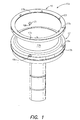
- FIG. 1 is an exploded perspective view of a first aspect of an inventive susceptor 11a.
- the susceptor 11a comprises a substrate support 13, adapted for pin and slot coupling with an edge ring, such as purge ring 15.
- the substrate support 13 comprises three pins 19a-c which extend upwardly from the top surface of substrate support 13.
- the bottom surface of the purge ring 15 comprises three hollow regions or slots 17 positioned to interface with the three pins 19a-c.
- the substrate support 13 comprises a central wafer supporting surface 13a, and the three pins 19 are equally spaced radially around the substrate supporting surface 13a.
- Each of the slots 17 is at least as wide as the corresponding pin 19, and extends radially outward from the center of the substrate supporting surface 13a, in the direction in which the substrate support expands and contracts during thermal cycling.
- the substrate support 13 is preferably made of a metal such as aluminum, as is conventional.
- the purge ring 15 is made of a material having a lower CTE than the CTE of the substrate support material.
- the purge ring is made of ceramic.
- the slots 17 extend a length which is sufficient to compensate for the difference between the CTE of the substrate support material and the CTE of the purge ring material, over the range of process temperatures to which the susceptor lla is exposed.
- each pin 19 is surrounded by a pad 21 made of a thermally insulating material, so as to achieve thermal insulation between the substrate support 13 and the purge ring 15, as further described below with reference to FIG. 2.
- the pads 21 are preferably made of a highly polished ceramic and therefore allow the purge ring 15 to slide easily therealong while minimizing particle generation.
- the purge ring 15 may further include a plurality of wafer guide pins 23 to facilitate accurate wafer placement, as is disclosed in U.S. Patent Application Serial No. 09/103,462 filed June 24,1998 (incorporated herein in its entirety by this reference).
- FIG. 2 is a side view, in pertinent part, of the first aspect of the inventive susceptor 11a, having a wafer W positioned thereon.
- the substrate support 13, the purge ring 15 and the slots 17 are configured such that with use of the pad 21, no direct contact exists between the substrate support 13 and the purge ring 15.
- the purge ring 15 experiences less thermal stress then would otherwise result if the purge ring 15 were to directly contact the typically higher temperature substrate support 13.
- the slot 17 has a depth greater than the length of the pin 19 to reduce thermal conduction from the substrate support 13 to the purge ring 15, via the pin 19.
- the slots 17 extend radially outward relative to the center of the substrate supporting surface 13 and preferably are each just slightly wider than the respective pin 19, thus preventing the purge ring 15 from moving laterally as a result of thermal cycling induced expansion and contraction more than the distance required for clearance between the slot 17 and the pin 19 pair. In this manner the pins also provide rotational alignment.
- the substrate support 13 comprises a purge gas delivery channel 25 and a diffuser ring 13b which couples purge gas from the purge gas delivery channel 25 through a purge gas distribution channel 27 defined by an inner edge of the diffuser ring 13b and an outer edge of the substrate support 13, and then through a plurality of small orifices O formed in the diffuser ring 13b to a lower edge of the purge ring 15.
- the wafer W is positioned on the wafer supporting surface 13a such that the edge of the wafer W is positioned adjacent the outlet of the purge slot 29.
- the susceptor is heated to a temperature in the range of 350° to 475°C, typically by a heating coil embedded in or contacted with the underside of, the susceptor.
- the susceptor is typically allowed to cool back to ambient temperatures.
- This temperature change causes thermal expansion and contraction of the chamber elements, including the substrate support and the purge ring.
- thermal cycling which occurs during CVD processing, and the resulting expansion and contraction of the substrate support 13 and the diffuser ring 13b, thermally induced stresses are not imposed upon the purge ring, as it (and the pins supporting it) can move radially as the temperature changes, due to the pin and slot coupling.
- Any thermally induced expansion of the gap between the purge ring and the wafer is insignificant. Accordingly edge deposition is more uniformly and reliably prevented.
- the purge ring 15 may be easily lifted off the pins 19 for routine cleaning or replacement. Accordingly downtime is minimized.
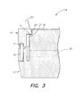
- FIG. 3 is a side view, in pertinent part, of a second aspect of the inventive susceptor.
- the inventive susceptor 11b of FIG. 3 is similar to the susceptor 11a of FIG. 2, except the substrate support 13 of FIG. 2 does not comprise the diffuser ring 13b. Instead the purge gas delivery channel 25 delivers purge gas to a purge gas distribution channel 27 which is defined by an inner edge of the purge ring 15 and an outer edge of the substrate support 13, as is the more narrowly defined purge gas slot 29.
- the embodiment of FIG. 3 requires fewer parts, and, replaces the orifices O (of FIG. 1) with a restrictor gap R.
- the restrictor gap R is formed by a horizontal notch in the substrate support 13 and a corresponding horizontal protrusion in the purge ring 15.
- the size of the restrictor gap R is determined by the respective vertical dimensions of the substrate support 13 and the purge ring 15 to the horizontal notch or protrusion, and by the thickness of the pad 21.
- the embodiment of FIG. 3 therefore reduces the clogging which may be experienced by the orifices O of the FIG. 1 embodiment as the restrictor gap R which expands radially around the substrate support in a continuum is less likely to clog than are the plurality of orifices O.
- the FIG. 3 embodiment also reduces the probability of differential expansion therebetween and the resultant particle generation.
- the purge ring 15 rests on the insulator pads 21 and is aligned by the pins 19.
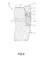
- FIG. 4 is a side view, in pertinent part, of a third aspect of the inventive susceptor.
- the purge ring 15 of the inventive susceptor 11c has a plurality of pins 19 (only one shown) which extend downward from the bottom surface of the purge ring 15.
- the pins 19 are pressed into the purge ring 15 and the pads 21 are secured to the pins 19 in the same manner, or maybe integral to the pins 19.
- the pins 19 are inserted within a corresponding slot 17 located on the substrate support 13.
- the slots 17 are formed in the diffuser ring portion 13b of the substrate support 13.
- FIG. 4 shows that the positions of the pins 19 and the slots 17 may be switched, and still achieve the advantages of pin and slot coupling.
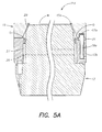
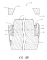
- FIGS. 5A and 5B are side views, in pertinent part, of a fourth aspect of the inventive susceptor 11d.
- the purge ring 15 of FIGS. 5A and 5B is configured such that its inner edge 15a overhangs the edge of the wafer W.
- the purge ring 15 functions as both a purge ring and a shadow ring (overhanging or shadowing the wafer's edge), as is known in the art.
- the pin and slot coupling of FIGS. 5A and 5B allows the substrate support 13 to expand and contract without affecting the shape or position of the purge/shadow ring 15, as described above with reference to FIGS. 2 and 3.
- FIG. 5A shows the purge/shadow ring 15 in a process position
- 5B shows the purge/shadow ring 15 in a wafer transfer position. Because shadow rings overlap the wafer's edge, they are conventionally supported in a wafer transfer position above the substrate support 13 (e.g., by a hanger or lip which protrudes from the chamber wall) while a wafer W is placed on or extracted from the substrate support 13. After a wafer is placed on the substrate support 13 the substrate support 13 elevates, transferring the shadow ring from the lip to the substrate support 13 as further described below.
- Conventional substrate supports whether to be used with a purge and/or shadow ring are initially lowered to a wafer transfer position.
- a wafer handler then carries a wafer into position above the substrate support 13; the substrate support 13 elevates and the lift pins thereof (not shown) lift the wafer off the wafer handler. Thereafter the wafer handler retracts and, if a shadow ring is employed, the substrate support 13 further elevates to lift the shadow ring, supported above the substrate support 13 (FIG. 5B) by the walls of the processing chamber (not shown), off of its support.
- FIG. 6 is a side view in pertinent part of a fifth aspect of the inventive susceptor.
- the inventive susceptor 11e is configured to facilitate access to the purge gas distribution channel 25 for cleaning.
- the surface of the substrate support 13 in which the pin 19 (or in an alternative embodiment, the slot 17) is located is below the outlet of the purge gas distribution channel 25.
- the purge gas distribution channel 25 may be angled upwardly (preferably between 0° and 30°), as shown in FIG. 6.
- a chamber such as the chamber described in commonly assigned U.S. Patent Application Serial No. 09/103,462 filed June 24, 1998 (incorporated herein in its entirety ), when employing the inventive susceptor of FIGS. 1 through 5, provides superior edge deposition prevention and increased throughput as compared to conventional deposition chambers (CVD, PVD, etc.).
- the inventive susceptor comprises pin and slot coupling between any type of edge ring (purge and/or shadow), whether the pins are located on the substrate support or the ring.
- edge ring purge and/or shadow
- each of the figures shows the use of thermally insulating pads these pads are optional.
- a heating element may be included in the susceptor, as is conventionally known.
- each of the gas delivery channels 25 of the various embodiments of the invention preferably open into a purge gas distribution channel 27 which also extends somewhat below the opening of the gas delivery channel 25 (as shown in each of the figures), so as to create a buffer channel which ensures more even distribution of the purge gas to the purge slots 29.
- pin and slot are to be broadly interpreted to include shapes other than the straight pins and slots shown (e.g., rectangular keys, etc.).
- purge or purge/shadow rings can be advantageously removably coupled to a substrate support, by mechanisms other than pin and slot coupling. Any removably coupled purge ring will benefit from the exposed outlet of the purge gas delivery channel and the upwardly angled purge gas delivery channel.
- a susceptor whether or not having a removably coupled purge ring can benefit from the definition of a purge gas distribution channel having a restrictor gap between the substrate support and the purge ring.
- these aspects of the invention should not be respectively limited to pin and slot coupling or to removably coupled purge rings.
Landscapes
- Engineering & Computer Science (AREA)
- Physics & Mathematics (AREA)
- Condensed Matter Physics & Semiconductors (AREA)
- General Physics & Mathematics (AREA)
- Manufacturing & Machinery (AREA)
- Computer Hardware Design (AREA)
- Microelectronics & Electronic Packaging (AREA)
- Power Engineering (AREA)
- Chemical & Material Sciences (AREA)
- General Chemical & Material Sciences (AREA)
- Chemical Kinetics & Catalysis (AREA)
- Materials Engineering (AREA)
- Mechanical Engineering (AREA)
- Metallurgy (AREA)
- Organic Chemistry (AREA)
- Chemical Vapour Deposition (AREA)
- Container, Conveyance, Adherence, Positioning, Of Wafer (AREA)
Applications Claiming Priority (2)
| Application Number | Priority Date | Filing Date | Title |
|---|---|---|---|
| US09/387,928 US6375748B1 (en) | 1999-09-01 | 1999-09-01 | Method and apparatus for preventing edge deposition |
| US387928 | 1999-09-01 |
Publications (1)
| Publication Number | Publication Date |
|---|---|
| EP1081744A2 true EP1081744A2 (en) | 2001-03-07 |
Family
ID=23531894
Family Applications (1)
| Application Number | Title | Priority Date | Filing Date |
|---|---|---|---|
| EP00307473A Withdrawn EP1081744A2 (en) | 1999-09-01 | 2000-08-31 | Method and apparatus for preventing edge deposition |
Country Status (6)
| Country | Link |
|---|---|
| US (1) | US6375748B1 (enExample) |
| EP (1) | EP1081744A2 (enExample) |
| JP (1) | JP4729160B2 (enExample) |
| KR (2) | KR100852098B1 (enExample) |
| SG (1) | SG93262A1 (enExample) |
| TW (1) | TW471009B (enExample) |
Cited By (4)
| Publication number | Priority date | Publication date | Assignee | Title |
|---|---|---|---|---|
| WO2014191623A1 (en) * | 2013-05-29 | 2014-12-04 | Beneq Oy | Substrate holder, arrangement and substrate carrier for supporting substrates |
| WO2016003599A1 (en) * | 2014-07-03 | 2016-01-07 | Applied Materials, Inc. | Substrate support with more uniform edge purge |
| CN109256357A (zh) * | 2017-07-13 | 2019-01-22 | 北京北方华创微电子装备有限公司 | 高温静电卡盘 |
| CN109767968A (zh) * | 2018-12-17 | 2019-05-17 | 北京北方华创微电子装备有限公司 | 下电极结构及反应腔室 |
Families Citing this family (193)
| Publication number | Priority date | Publication date | Assignee | Title |
|---|---|---|---|---|
| JP4260307B2 (ja) * | 1999-09-28 | 2009-04-30 | 芝浦メカトロニクス株式会社 | 気相成長装置 |
| US6589352B1 (en) * | 1999-12-10 | 2003-07-08 | Applied Materials, Inc. | Self aligning non contact shadow ring process kit |
| JP4419237B2 (ja) * | 1999-12-22 | 2010-02-24 | 東京エレクトロン株式会社 | 成膜装置及び被処理体の処理方法 |
| US6702900B2 (en) * | 2001-03-22 | 2004-03-09 | Taiwan Semiconductor Manufacturing Co., Ltd. | Wafer chuck for producing an inert gas blanket and method for using |
| US20040083976A1 (en) * | 2002-09-25 | 2004-05-06 | Silterra Malaysia Sdn. Bhd. | Modified deposition ring to eliminate backside and wafer edge coating |
| US20050092255A1 (en) * | 2003-11-04 | 2005-05-05 | Taiwan Semiconductor Manufacturing Co. Ltd. | Edge-contact wafer holder for CMP load/unload station |
| KR101248182B1 (ko) * | 2004-02-26 | 2013-03-27 | 어플라이드 머티어리얼스, 인코포레이티드 | Feol 제조를 위한 인시튜 세정 챔버 |
| US20050230350A1 (en) * | 2004-02-26 | 2005-10-20 | Applied Materials, Inc. | In-situ dry clean chamber for front end of line fabrication |
| US20060000802A1 (en) * | 2004-06-30 | 2006-01-05 | Ajay Kumar | Method and apparatus for photomask plasma etching |
| US8349128B2 (en) | 2004-06-30 | 2013-01-08 | Applied Materials, Inc. | Method and apparatus for stable plasma processing |
| US20060151116A1 (en) * | 2005-01-12 | 2006-07-13 | Taiwan Semiconductor Manufacturing Co., Ltd. | Focus rings, apparatus in chamber, contact hole and method of forming contact hole |
| US20070065597A1 (en) * | 2005-09-15 | 2007-03-22 | Asm Japan K.K. | Plasma CVD film formation apparatus provided with mask |
| US7909961B2 (en) * | 2006-10-30 | 2011-03-22 | Applied Materials, Inc. | Method and apparatus for photomask plasma etching |
| US7943005B2 (en) | 2006-10-30 | 2011-05-17 | Applied Materials, Inc. | Method and apparatus for photomask plasma etching |
| WO2008139871A1 (ja) * | 2007-05-09 | 2008-11-20 | Ulvac, Inc. | パージガスアセンブリ |
| JP5260023B2 (ja) * | 2007-10-19 | 2013-08-14 | 三菱重工業株式会社 | プラズマ成膜装置 |
| JP2009277720A (ja) * | 2008-05-12 | 2009-11-26 | Nec Electronics Corp | 半導体装置の製造方法及びエッチング装置 |
| WO2011017226A2 (en) * | 2009-08-07 | 2011-02-10 | Applied Materials, Inc. | Compound lift pin tip with temperature compensated attachment feature |
| JP5992334B2 (ja) * | 2009-12-31 | 2016-09-14 | アプライド マテリアルズ インコーポレイテッドApplied Materials,Incorporated | ウエハのエッジおよび斜面の堆積を修正するためのシャドウリング |
| US9324576B2 (en) | 2010-05-27 | 2016-04-26 | Applied Materials, Inc. | Selective etch for silicon films |
| CN103069542A (zh) * | 2010-08-20 | 2013-04-24 | 应用材料公司 | 延长寿命的沉积环 |
| US10283321B2 (en) | 2011-01-18 | 2019-05-07 | Applied Materials, Inc. | Semiconductor processing system and methods using capacitively coupled plasma |
| US8771539B2 (en) | 2011-02-22 | 2014-07-08 | Applied Materials, Inc. | Remotely-excited fluorine and water vapor etch |
| US9064815B2 (en) | 2011-03-14 | 2015-06-23 | Applied Materials, Inc. | Methods for etch of metal and metal-oxide films |
| US8999856B2 (en) | 2011-03-14 | 2015-04-07 | Applied Materials, Inc. | Methods for etch of sin films |
| US8771536B2 (en) | 2011-08-01 | 2014-07-08 | Applied Materials, Inc. | Dry-etch for silicon-and-carbon-containing films |
| US8679982B2 (en) | 2011-08-26 | 2014-03-25 | Applied Materials, Inc. | Selective suppression of dry-etch rate of materials containing both silicon and oxygen |
| US8679983B2 (en) | 2011-09-01 | 2014-03-25 | Applied Materials, Inc. | Selective suppression of dry-etch rate of materials containing both silicon and nitrogen |
| US8927390B2 (en) | 2011-09-26 | 2015-01-06 | Applied Materials, Inc. | Intrench profile |
| US8808563B2 (en) | 2011-10-07 | 2014-08-19 | Applied Materials, Inc. | Selective etch of silicon by way of metastable hydrogen termination |
| WO2013070436A1 (en) | 2011-11-08 | 2013-05-16 | Applied Materials, Inc. | Methods of reducing substrate dislocation during gapfill processing |
| US8980767B2 (en) * | 2012-01-13 | 2015-03-17 | Applied Materials, Inc. | Methods and apparatus for processing a substrate |
| US9267739B2 (en) | 2012-07-18 | 2016-02-23 | Applied Materials, Inc. | Pedestal with multi-zone temperature control and multiple purge capabilities |
| US9373517B2 (en) | 2012-08-02 | 2016-06-21 | Applied Materials, Inc. | Semiconductor processing with DC assisted RF power for improved control |
| US9034770B2 (en) | 2012-09-17 | 2015-05-19 | Applied Materials, Inc. | Differential silicon oxide etch |
| US9023734B2 (en) | 2012-09-18 | 2015-05-05 | Applied Materials, Inc. | Radical-component oxide etch |
| US9390937B2 (en) | 2012-09-20 | 2016-07-12 | Applied Materials, Inc. | Silicon-carbon-nitride selective etch |
| US9132436B2 (en) | 2012-09-21 | 2015-09-15 | Applied Materials, Inc. | Chemical control features in wafer process equipment |
| US8765574B2 (en) | 2012-11-09 | 2014-07-01 | Applied Materials, Inc. | Dry etch process |
| US8969212B2 (en) | 2012-11-20 | 2015-03-03 | Applied Materials, Inc. | Dry-etch selectivity |
| US8980763B2 (en) | 2012-11-30 | 2015-03-17 | Applied Materials, Inc. | Dry-etch for selective tungsten removal |
| US9064816B2 (en) | 2012-11-30 | 2015-06-23 | Applied Materials, Inc. | Dry-etch for selective oxidation removal |
| US9111877B2 (en) | 2012-12-18 | 2015-08-18 | Applied Materials, Inc. | Non-local plasma oxide etch |
| US8921234B2 (en) | 2012-12-21 | 2014-12-30 | Applied Materials, Inc. | Selective titanium nitride etching |
| CN103928291B (zh) * | 2013-01-11 | 2017-06-13 | 无锡华润上华科技有限公司 | 半导体面电阻均匀性的改善方法 |
| US10256079B2 (en) | 2013-02-08 | 2019-04-09 | Applied Materials, Inc. | Semiconductor processing systems having multiple plasma configurations |
| US9362130B2 (en) | 2013-03-01 | 2016-06-07 | Applied Materials, Inc. | Enhanced etching processes using remote plasma sources |
| US9040422B2 (en) | 2013-03-05 | 2015-05-26 | Applied Materials, Inc. | Selective titanium nitride removal |
| US8801952B1 (en) | 2013-03-07 | 2014-08-12 | Applied Materials, Inc. | Conformal oxide dry etch |
| US10170282B2 (en) | 2013-03-08 | 2019-01-01 | Applied Materials, Inc. | Insulated semiconductor faceplate designs |
| US20140271097A1 (en) | 2013-03-15 | 2014-09-18 | Applied Materials, Inc. | Processing systems and methods for halide scavenging |
| US8895449B1 (en) | 2013-05-16 | 2014-11-25 | Applied Materials, Inc. | Delicate dry clean |
| US9114438B2 (en) | 2013-05-21 | 2015-08-25 | Applied Materials, Inc. | Copper residue chamber clean |
| US9493879B2 (en) | 2013-07-12 | 2016-11-15 | Applied Materials, Inc. | Selective sputtering for pattern transfer |
| US9773648B2 (en) | 2013-08-30 | 2017-09-26 | Applied Materials, Inc. | Dual discharge modes operation for remote plasma |
| US8956980B1 (en) | 2013-09-16 | 2015-02-17 | Applied Materials, Inc. | Selective etch of silicon nitride |
| US8951429B1 (en) | 2013-10-29 | 2015-02-10 | Applied Materials, Inc. | Tungsten oxide processing |
| US9236265B2 (en) | 2013-11-04 | 2016-01-12 | Applied Materials, Inc. | Silicon germanium processing |
| US9576809B2 (en) | 2013-11-04 | 2017-02-21 | Applied Materials, Inc. | Etch suppression with germanium |
| US9520303B2 (en) | 2013-11-12 | 2016-12-13 | Applied Materials, Inc. | Aluminum selective etch |
| US9245762B2 (en) | 2013-12-02 | 2016-01-26 | Applied Materials, Inc. | Procedure for etch rate consistency |
| US9117855B2 (en) | 2013-12-04 | 2015-08-25 | Applied Materials, Inc. | Polarity control for remote plasma |
| US9287095B2 (en) | 2013-12-17 | 2016-03-15 | Applied Materials, Inc. | Semiconductor system assemblies and methods of operation |
| US9263278B2 (en) | 2013-12-17 | 2016-02-16 | Applied Materials, Inc. | Dopant etch selectivity control |
| US9190293B2 (en) | 2013-12-18 | 2015-11-17 | Applied Materials, Inc. | Even tungsten etch for high aspect ratio trenches |
| US9287134B2 (en) | 2014-01-17 | 2016-03-15 | Applied Materials, Inc. | Titanium oxide etch |
| US9396989B2 (en) | 2014-01-27 | 2016-07-19 | Applied Materials, Inc. | Air gaps between copper lines |
| US9293568B2 (en) | 2014-01-27 | 2016-03-22 | Applied Materials, Inc. | Method of fin patterning |
| US9385028B2 (en) | 2014-02-03 | 2016-07-05 | Applied Materials, Inc. | Air gap process |
| US9499898B2 (en) | 2014-03-03 | 2016-11-22 | Applied Materials, Inc. | Layered thin film heater and method of fabrication |
| US9299575B2 (en) | 2014-03-17 | 2016-03-29 | Applied Materials, Inc. | Gas-phase tungsten etch |
| US9299537B2 (en) | 2014-03-20 | 2016-03-29 | Applied Materials, Inc. | Radial waveguide systems and methods for post-match control of microwaves |
| US9299538B2 (en) | 2014-03-20 | 2016-03-29 | Applied Materials, Inc. | Radial waveguide systems and methods for post-match control of microwaves |
| US9136273B1 (en) | 2014-03-21 | 2015-09-15 | Applied Materials, Inc. | Flash gate air gap |
| US9903020B2 (en) | 2014-03-31 | 2018-02-27 | Applied Materials, Inc. | Generation of compact alumina passivation layers on aluminum plasma equipment components |
| US9269590B2 (en) | 2014-04-07 | 2016-02-23 | Applied Materials, Inc. | Spacer formation |
| US9309598B2 (en) | 2014-05-28 | 2016-04-12 | Applied Materials, Inc. | Oxide and metal removal |
| US9847289B2 (en) | 2014-05-30 | 2017-12-19 | Applied Materials, Inc. | Protective via cap for improved interconnect performance |
| US9378969B2 (en) | 2014-06-19 | 2016-06-28 | Applied Materials, Inc. | Low temperature gas-phase carbon removal |
| US9406523B2 (en) | 2014-06-19 | 2016-08-02 | Applied Materials, Inc. | Highly selective doped oxide removal method |
| US9425058B2 (en) | 2014-07-24 | 2016-08-23 | Applied Materials, Inc. | Simplified litho-etch-litho-etch process |
| US9496167B2 (en) | 2014-07-31 | 2016-11-15 | Applied Materials, Inc. | Integrated bit-line airgap formation and gate stack post clean |
| US9159606B1 (en) | 2014-07-31 | 2015-10-13 | Applied Materials, Inc. | Metal air gap |
| US9378978B2 (en) | 2014-07-31 | 2016-06-28 | Applied Materials, Inc. | Integrated oxide recess and floating gate fin trimming |
| US9165786B1 (en) | 2014-08-05 | 2015-10-20 | Applied Materials, Inc. | Integrated oxide and nitride recess for better channel contact in 3D architectures |
| US9659753B2 (en) | 2014-08-07 | 2017-05-23 | Applied Materials, Inc. | Grooved insulator to reduce leakage current |
| US9553102B2 (en) | 2014-08-19 | 2017-01-24 | Applied Materials, Inc. | Tungsten separation |
| US9355856B2 (en) | 2014-09-12 | 2016-05-31 | Applied Materials, Inc. | V trench dry etch |
| US9368364B2 (en) | 2014-09-24 | 2016-06-14 | Applied Materials, Inc. | Silicon etch process with tunable selectivity to SiO2 and other materials |
| US9478434B2 (en) | 2014-09-24 | 2016-10-25 | Applied Materials, Inc. | Chlorine-based hardmask removal |
| US9613822B2 (en) | 2014-09-25 | 2017-04-04 | Applied Materials, Inc. | Oxide etch selectivity enhancement |
| US9355922B2 (en) | 2014-10-14 | 2016-05-31 | Applied Materials, Inc. | Systems and methods for internal surface conditioning in plasma processing equipment |
| US9966240B2 (en) | 2014-10-14 | 2018-05-08 | Applied Materials, Inc. | Systems and methods for internal surface conditioning assessment in plasma processing equipment |
| US11637002B2 (en) | 2014-11-26 | 2023-04-25 | Applied Materials, Inc. | Methods and systems to enhance process uniformity |
| US9299583B1 (en) | 2014-12-05 | 2016-03-29 | Applied Materials, Inc. | Aluminum oxide selective etch |
| US10573496B2 (en) | 2014-12-09 | 2020-02-25 | Applied Materials, Inc. | Direct outlet toroidal plasma source |
| US10224210B2 (en) | 2014-12-09 | 2019-03-05 | Applied Materials, Inc. | Plasma processing system with direct outlet toroidal plasma source |
| US9502258B2 (en) | 2014-12-23 | 2016-11-22 | Applied Materials, Inc. | Anisotropic gap etch |
| US9343272B1 (en) | 2015-01-08 | 2016-05-17 | Applied Materials, Inc. | Self-aligned process |
| US11257693B2 (en) | 2015-01-09 | 2022-02-22 | Applied Materials, Inc. | Methods and systems to improve pedestal temperature control |
| US9373522B1 (en) | 2015-01-22 | 2016-06-21 | Applied Mateials, Inc. | Titanium nitride removal |
| US9449846B2 (en) | 2015-01-28 | 2016-09-20 | Applied Materials, Inc. | Vertical gate separation |
| US9728437B2 (en) | 2015-02-03 | 2017-08-08 | Applied Materials, Inc. | High temperature chuck for plasma processing systems |
| US20160225652A1 (en) | 2015-02-03 | 2016-08-04 | Applied Materials, Inc. | Low temperature chuck for plasma processing systems |
| US9881805B2 (en) | 2015-03-02 | 2018-01-30 | Applied Materials, Inc. | Silicon selective removal |
| US9741593B2 (en) | 2015-08-06 | 2017-08-22 | Applied Materials, Inc. | Thermal management systems and methods for wafer processing systems |
| US9691645B2 (en) | 2015-08-06 | 2017-06-27 | Applied Materials, Inc. | Bolted wafer chuck thermal management systems and methods for wafer processing systems |
| US9349605B1 (en) | 2015-08-07 | 2016-05-24 | Applied Materials, Inc. | Oxide etch selectivity systems and methods |
| US10504700B2 (en) | 2015-08-27 | 2019-12-10 | Applied Materials, Inc. | Plasma etching systems and methods with secondary plasma injection |
| KR102689380B1 (ko) | 2016-01-26 | 2024-07-26 | 어플라이드 머티어리얼스, 인코포레이티드 | 웨이퍼 에지 링 리프팅 솔루션 |
| JP6888007B2 (ja) | 2016-01-26 | 2021-06-16 | アプライド マテリアルズ インコーポレイテッドApplied Materials,Incorporated | ウェハエッジリングの持ち上げに関する解決 |
| TWI689619B (zh) * | 2016-04-01 | 2020-04-01 | 美商應用材料股份有限公司 | 用於提供均勻流動的氣體的設備及方法 |
| US10522371B2 (en) | 2016-05-19 | 2019-12-31 | Applied Materials, Inc. | Systems and methods for improved semiconductor etching and component protection |
| US10504754B2 (en) | 2016-05-19 | 2019-12-10 | Applied Materials, Inc. | Systems and methods for improved semiconductor etching and component protection |
| US9865484B1 (en) | 2016-06-29 | 2018-01-09 | Applied Materials, Inc. | Selective etch using material modification and RF pulsing |
| US10062575B2 (en) | 2016-09-09 | 2018-08-28 | Applied Materials, Inc. | Poly directional etch by oxidation |
| US10629473B2 (en) | 2016-09-09 | 2020-04-21 | Applied Materials, Inc. | Footing removal for nitride spacer |
| US9934942B1 (en) | 2016-10-04 | 2018-04-03 | Applied Materials, Inc. | Chamber with flow-through source |
| US10546729B2 (en) | 2016-10-04 | 2020-01-28 | Applied Materials, Inc. | Dual-channel showerhead with improved profile |
| US10062585B2 (en) | 2016-10-04 | 2018-08-28 | Applied Materials, Inc. | Oxygen compatible plasma source |
| US9721789B1 (en) | 2016-10-04 | 2017-08-01 | Applied Materials, Inc. | Saving ion-damaged spacers |
| US10062579B2 (en) | 2016-10-07 | 2018-08-28 | Applied Materials, Inc. | Selective SiN lateral recess |
| US9947549B1 (en) | 2016-10-10 | 2018-04-17 | Applied Materials, Inc. | Cobalt-containing material removal |
| US10163696B2 (en) | 2016-11-11 | 2018-12-25 | Applied Materials, Inc. | Selective cobalt removal for bottom up gapfill |
| US9768034B1 (en) | 2016-11-11 | 2017-09-19 | Applied Materials, Inc. | Removal methods for high aspect ratio structures |
| US10242908B2 (en) | 2016-11-14 | 2019-03-26 | Applied Materials, Inc. | Airgap formation with damage-free copper |
| US10026621B2 (en) | 2016-11-14 | 2018-07-17 | Applied Materials, Inc. | SiN spacer profile patterning |
| US10566206B2 (en) | 2016-12-27 | 2020-02-18 | Applied Materials, Inc. | Systems and methods for anisotropic material breakthrough |
| US10553404B2 (en) | 2017-02-01 | 2020-02-04 | Applied Materials, Inc. | Adjustable extended electrode for edge uniformity control |
| US10431429B2 (en) | 2017-02-03 | 2019-10-01 | Applied Materials, Inc. | Systems and methods for radial and azimuthal control of plasma uniformity |
| US10403507B2 (en) | 2017-02-03 | 2019-09-03 | Applied Materials, Inc. | Shaped etch profile with oxidation |
| US10043684B1 (en) | 2017-02-06 | 2018-08-07 | Applied Materials, Inc. | Self-limiting atomic thermal etching systems and methods |
| US10319739B2 (en) | 2017-02-08 | 2019-06-11 | Applied Materials, Inc. | Accommodating imperfectly aligned memory holes |
| US10943834B2 (en) | 2017-03-13 | 2021-03-09 | Applied Materials, Inc. | Replacement contact process |
| US10319649B2 (en) | 2017-04-11 | 2019-06-11 | Applied Materials, Inc. | Optical emission spectroscopy (OES) for remote plasma monitoring |
| US11276590B2 (en) | 2017-05-17 | 2022-03-15 | Applied Materials, Inc. | Multi-zone semiconductor substrate supports |
| JP7176860B6 (ja) | 2017-05-17 | 2022-12-16 | アプライド マテリアルズ インコーポレイテッド | 前駆体の流れを改善する半導体処理チャンバ |
| US11276559B2 (en) | 2017-05-17 | 2022-03-15 | Applied Materials, Inc. | Semiconductor processing chamber for multiple precursor flow |
| US10049891B1 (en) | 2017-05-31 | 2018-08-14 | Applied Materials, Inc. | Selective in situ cobalt residue removal |
| US10497579B2 (en) | 2017-05-31 | 2019-12-03 | Applied Materials, Inc. | Water-free etching methods |
| US10920320B2 (en) | 2017-06-16 | 2021-02-16 | Applied Materials, Inc. | Plasma health determination in semiconductor substrate processing reactors |
| US10541246B2 (en) | 2017-06-26 | 2020-01-21 | Applied Materials, Inc. | 3D flash memory cells which discourage cross-cell electrical tunneling |
| US10727080B2 (en) | 2017-07-07 | 2020-07-28 | Applied Materials, Inc. | Tantalum-containing material removal |
| US10541184B2 (en) | 2017-07-11 | 2020-01-21 | Applied Materials, Inc. | Optical emission spectroscopic techniques for monitoring etching |
| US10354889B2 (en) | 2017-07-17 | 2019-07-16 | Applied Materials, Inc. | Non-halogen etching of silicon-containing materials |
| US10043674B1 (en) | 2017-08-04 | 2018-08-07 | Applied Materials, Inc. | Germanium etching systems and methods |
| US10170336B1 (en) | 2017-08-04 | 2019-01-01 | Applied Materials, Inc. | Methods for anisotropic control of selective silicon removal |
| US10297458B2 (en) | 2017-08-07 | 2019-05-21 | Applied Materials, Inc. | Process window widening using coated parts in plasma etch processes |
| US11075105B2 (en) | 2017-09-21 | 2021-07-27 | Applied Materials, Inc. | In-situ apparatus for semiconductor process module |
| US10128086B1 (en) | 2017-10-24 | 2018-11-13 | Applied Materials, Inc. | Silicon pretreatment for nitride removal |
| US10283324B1 (en) | 2017-10-24 | 2019-05-07 | Applied Materials, Inc. | Oxygen treatment for nitride etching |
| US10256112B1 (en) | 2017-12-08 | 2019-04-09 | Applied Materials, Inc. | Selective tungsten removal |
| US10903054B2 (en) | 2017-12-19 | 2021-01-26 | Applied Materials, Inc. | Multi-zone gas distribution systems and methods |
| US11043400B2 (en) | 2017-12-21 | 2021-06-22 | Applied Materials, Inc. | Movable and removable process kit |
| US11328909B2 (en) | 2017-12-22 | 2022-05-10 | Applied Materials, Inc. | Chamber conditioning and removal processes |
| US10854426B2 (en) | 2018-01-08 | 2020-12-01 | Applied Materials, Inc. | Metal recess for semiconductor structures |
| US12293902B2 (en) | 2018-01-19 | 2025-05-06 | Applied Materials, Inc. | Process kit for a substrate support |
| US10679870B2 (en) | 2018-02-15 | 2020-06-09 | Applied Materials, Inc. | Semiconductor processing chamber multistage mixing apparatus |
| US10964512B2 (en) | 2018-02-15 | 2021-03-30 | Applied Materials, Inc. | Semiconductor processing chamber multistage mixing apparatus and methods |
| TWI766433B (zh) | 2018-02-28 | 2022-06-01 | 美商應用材料股份有限公司 | 形成氣隙的系統及方法 |
| US10593560B2 (en) | 2018-03-01 | 2020-03-17 | Applied Materials, Inc. | Magnetic induction plasma source for semiconductor processes and equipment |
| US10319600B1 (en) | 2018-03-12 | 2019-06-11 | Applied Materials, Inc. | Thermal silicon etch |
| US10497573B2 (en) | 2018-03-13 | 2019-12-03 | Applied Materials, Inc. | Selective atomic layer etching of semiconductor materials |
| US10573527B2 (en) | 2018-04-06 | 2020-02-25 | Applied Materials, Inc. | Gas-phase selective etching systems and methods |
| US10490406B2 (en) | 2018-04-10 | 2019-11-26 | Appled Materials, Inc. | Systems and methods for material breakthrough |
| US10699879B2 (en) | 2018-04-17 | 2020-06-30 | Applied Materials, Inc. | Two piece electrode assembly with gap for plasma control |
| US10886137B2 (en) | 2018-04-30 | 2021-01-05 | Applied Materials, Inc. | Selective nitride removal |
| US10790123B2 (en) | 2018-05-28 | 2020-09-29 | Applied Materials, Inc. | Process kit with adjustable tuning ring for edge uniformity control |
| US11935773B2 (en) | 2018-06-14 | 2024-03-19 | Applied Materials, Inc. | Calibration jig and calibration method |
| US10872778B2 (en) | 2018-07-06 | 2020-12-22 | Applied Materials, Inc. | Systems and methods utilizing solid-phase etchants |
| US10755941B2 (en) | 2018-07-06 | 2020-08-25 | Applied Materials, Inc. | Self-limiting selective etching systems and methods |
| US10672642B2 (en) | 2018-07-24 | 2020-06-02 | Applied Materials, Inc. | Systems and methods for pedestal configuration |
| US10892198B2 (en) | 2018-09-14 | 2021-01-12 | Applied Materials, Inc. | Systems and methods for improved performance in semiconductor processing |
| US11049755B2 (en) | 2018-09-14 | 2021-06-29 | Applied Materials, Inc. | Semiconductor substrate supports with embedded RF shield |
| US11062887B2 (en) | 2018-09-17 | 2021-07-13 | Applied Materials, Inc. | High temperature RF heater pedestals |
| US11417534B2 (en) | 2018-09-21 | 2022-08-16 | Applied Materials, Inc. | Selective material removal |
| US11682560B2 (en) | 2018-10-11 | 2023-06-20 | Applied Materials, Inc. | Systems and methods for hafnium-containing film removal |
| US11121002B2 (en) | 2018-10-24 | 2021-09-14 | Applied Materials, Inc. | Systems and methods for etching metals and metal derivatives |
| US11289310B2 (en) | 2018-11-21 | 2022-03-29 | Applied Materials, Inc. | Circuits for edge ring control in shaped DC pulsed plasma process device |
| US11437242B2 (en) | 2018-11-27 | 2022-09-06 | Applied Materials, Inc. | Selective removal of silicon-containing materials |
| US11721527B2 (en) | 2019-01-07 | 2023-08-08 | Applied Materials, Inc. | Processing chamber mixing systems |
| US10920319B2 (en) | 2019-01-11 | 2021-02-16 | Applied Materials, Inc. | Ceramic showerheads with conductive electrodes |
| WO2020214327A1 (en) | 2019-04-19 | 2020-10-22 | Applied Materials, Inc. | Ring removal from processing chamber |
| US12009236B2 (en) | 2019-04-22 | 2024-06-11 | Applied Materials, Inc. | Sensors and system for in-situ edge ring erosion monitor |
| US11823937B2 (en) * | 2019-08-19 | 2023-11-21 | Applied Materials, Inc. | Calibration of an aligner station of a processing system |
| JP7359000B2 (ja) * | 2020-01-20 | 2023-10-11 | 東京エレクトロン株式会社 | 基板を処理する装置、及び基板を処理する方法 |
| US11759954B2 (en) | 2020-03-17 | 2023-09-19 | Applied Materials, Inc. | Calibration of an electronics processing system |
| US20220049350A1 (en) * | 2020-08-13 | 2022-02-17 | Applied Materials, Inc. | Apparatus design for photoresist deposition |
| US20220108872A1 (en) * | 2020-10-05 | 2022-04-07 | Applied Materials, Inc. | Bevel backside deposition elimination |
| TWI749956B (zh) * | 2020-12-18 | 2021-12-11 | 天虹科技股份有限公司 | 薄膜沉積裝置 |
| CN112647054B (zh) * | 2020-12-23 | 2023-10-03 | 深圳市捷佳伟创新能源装备股份有限公司 | 双面镀膜系统以及双面镀膜方法 |
| US11561254B2 (en) * | 2021-05-27 | 2023-01-24 | Semilab Semiconductor Physics Laboratory Co., Ltd. | Topside contact device and method for characterization of high electron mobility transistor (HEMT) heterostructure on insulating and semi-insulating substrates |
| KR102876725B1 (ko) * | 2022-01-12 | 2025-10-27 | 베이징 나우라 마이크로일렉트로닉스 이큅먼트 씨오., 엘티디. | 반도체 공정 디바이스 및 이의 재치 장치 |
Family Cites Families (17)
| Publication number | Priority date | Publication date | Assignee | Title |
|---|---|---|---|---|
| US4911812A (en) | 1987-10-21 | 1990-03-27 | Hitachi, Ltd. | Plasma treating method and apparatus therefor |
| US5230741A (en) * | 1990-07-16 | 1993-07-27 | Novellus Systems, Inc. | Gas-based backside protection during substrate processing |
| US5304248A (en) * | 1990-12-05 | 1994-04-19 | Applied Materials, Inc. | Passive shield for CVD wafer processing which provides frontside edge exclusion and prevents backside depositions |
| US5326725A (en) * | 1993-03-11 | 1994-07-05 | Applied Materials, Inc. | Clamping ring and susceptor therefor |
| US5800686A (en) | 1993-04-05 | 1998-09-01 | Applied Materials, Inc. | Chemical vapor deposition chamber with substrate edge protection |
| US5556476A (en) * | 1994-02-23 | 1996-09-17 | Applied Materials, Inc. | Controlling edge deposition on semiconductor substrates |
| US5888304A (en) * | 1996-04-02 | 1999-03-30 | Applied Materials, Inc. | Heater with shadow ring and purge above wafer surface |
| US5766365A (en) * | 1994-02-23 | 1998-06-16 | Applied Materials, Inc. | Removable ring for controlling edge deposition in substrate processing apparatus |
| US5558717A (en) * | 1994-11-30 | 1996-09-24 | Applied Materials | CVD Processing chamber |
| JP3215599B2 (ja) * | 1995-06-02 | 2001-10-09 | 東芝セラミックス株式会社 | 熱処理用基板保持具、熱処理方法および熱処理装置 |
| US5697427A (en) * | 1995-12-22 | 1997-12-16 | Applied Materials, Inc. | Apparatus and method for cooling a substrate |
| US5863340A (en) * | 1996-05-08 | 1999-01-26 | Flanigan; Allen | Deposition ring anti-rotation apparatus |
| US5846332A (en) * | 1996-07-12 | 1998-12-08 | Applied Materials, Inc. | Thermally floating pedestal collar in a chemical vapor deposition chamber |
| TW350983B (en) * | 1996-10-15 | 1999-01-21 | Applied Materials Inc | Wafer edge deposition elimination |
| JP3796005B2 (ja) * | 1997-05-15 | 2006-07-12 | アプライド マテリアルズ インコーポレイテッド | マスク装置及び成膜装置 |
| JP3078506B2 (ja) * | 1997-06-26 | 2000-08-21 | 芝浦メカトロニクス株式会社 | 静電チャック装置及び載置台 |
| US5985033A (en) * | 1997-07-11 | 1999-11-16 | Applied Materials, Inc. | Apparatus and method for delivering a gas |
-
1999
- 1999-09-01 US US09/387,928 patent/US6375748B1/en not_active Expired - Lifetime
-
2000
- 2000-08-31 SG SG200005011A patent/SG93262A1/en unknown
- 2000-08-31 EP EP00307473A patent/EP1081744A2/en not_active Withdrawn
- 2000-09-01 KR KR1020000051588A patent/KR100852098B1/ko not_active Expired - Lifetime
- 2000-09-01 TW TW089117954A patent/TW471009B/zh not_active IP Right Cessation
- 2000-09-01 JP JP2000306815A patent/JP4729160B2/ja not_active Expired - Lifetime
-
2007
- 2007-06-13 KR KR1020070057641A patent/KR100867776B1/ko not_active Expired - Lifetime
Cited By (7)
| Publication number | Priority date | Publication date | Assignee | Title |
|---|---|---|---|---|
| WO2014191623A1 (en) * | 2013-05-29 | 2014-12-04 | Beneq Oy | Substrate holder, arrangement and substrate carrier for supporting substrates |
| WO2016003599A1 (en) * | 2014-07-03 | 2016-01-07 | Applied Materials, Inc. | Substrate support with more uniform edge purge |
| JP2017527984A (ja) * | 2014-07-03 | 2017-09-21 | アプライド マテリアルズ インコーポレイテッドApplied Materials,Incorporated | より均一なエッジパージを有する基板支持体 |
| CN109256357A (zh) * | 2017-07-13 | 2019-01-22 | 北京北方华创微电子装备有限公司 | 高温静电卡盘 |
| CN109256357B (zh) * | 2017-07-13 | 2020-06-19 | 北京北方华创微电子装备有限公司 | 高温静电卡盘 |
| CN109767968A (zh) * | 2018-12-17 | 2019-05-17 | 北京北方华创微电子装备有限公司 | 下电极结构及反应腔室 |
| CN109767968B (zh) * | 2018-12-17 | 2021-06-08 | 北京北方华创微电子装备有限公司 | 下电极结构及反应腔室 |
Also Published As
| Publication number | Publication date |
|---|---|
| US6375748B1 (en) | 2002-04-23 |
| KR20070070143A (ko) | 2007-07-03 |
| TW471009B (en) | 2002-01-01 |
| KR100867776B1 (ko) | 2008-11-10 |
| SG93262A1 (en) | 2002-12-17 |
| KR20010030222A (ko) | 2001-04-16 |
| JP2001203163A (ja) | 2001-07-27 |
| KR100852098B1 (ko) | 2008-08-13 |
| JP4729160B2 (ja) | 2011-07-20 |
Similar Documents
| Publication | Publication Date | Title |
|---|---|---|
| US6375748B1 (en) | Method and apparatus for preventing edge deposition | |
| US8342119B2 (en) | Self aligning non contact shadow ring process kit | |
| US6521292B1 (en) | Substrate support including purge ring having inner edge aligned to wafer edge | |
| US5888304A (en) | Heater with shadow ring and purge above wafer surface | |
| US6033480A (en) | Wafer edge deposition elimination | |
| US11136665B2 (en) | Shadow ring for modifying wafer edge and bevel deposition | |
| US7520969B2 (en) | Notched deposition ring | |
| US6368450B2 (en) | Processing apparatus | |
| US6146463A (en) | Apparatus and method for aligning a substrate on a support member | |
| KR102025330B1 (ko) | 웨이퍼 프로세싱 증착 차폐 컴포넌트들 | |
| EP0688888A2 (en) | Apparatus and method for substrate processing | |
| EP0747934A1 (en) | Apparatus for supporting substrates in processing chambers | |
| US20030132319A1 (en) | Showerhead assembly for a processing chamber | |
| JPH08236451A (ja) | 半導体基板のエッジ成膜の制御 | |
| KR20010082657A (ko) | 퍼지링용 결속장치 | |
| US11697877B2 (en) | High temperature face plate for deposition application | |
| EP1134791A2 (en) | Shadow ring with common guide member | |
| KR101011152B1 (ko) | 기판받침대를 가지는 막 형성 장치 | |
| US6503331B1 (en) | Tungsten chamber with stationary heater |
Legal Events
| Date | Code | Title | Description |
|---|---|---|---|
| PUAI | Public reference made under article 153(3) epc to a published international application that has entered the european phase |
Free format text: ORIGINAL CODE: 0009012 |
|
| AK | Designated contracting states |
Kind code of ref document: A2 Designated state(s): AT BE CH CY DE DK ES FI FR GB GR IE IT LI LU MC NL PT SE |
|
| AX | Request for extension of the european patent |
Free format text: AL;LT;LV;MK;RO;SI |
|
| RIN1 | Information on inventor provided before grant (corrected) |
Inventor name: UMOTOY, SALVADOR Inventor name: TRINH, SON NGOC Inventor name: MADAR, THOMAS A. Inventor name: CHANG, ANZHONG ANDREW Inventor name: LEI, LAWRENCE C. Inventor name: YUAN, XIAOXIONG JOHN Inventor name: YUDOVSKY, JOSEPH |
|
| STAA | Information on the status of an ep patent application or granted ep patent |
Free format text: STATUS: THE APPLICATION IS DEEMED TO BE WITHDRAWN |
|
| 18D | Application deemed to be withdrawn |
Effective date: 20040302 |