EP1062501B1 - Referenzelektrode - Google Patents
Referenzelektrode Download PDFInfo
- Publication number
- EP1062501B1 EP1062501B1 EP99911731A EP99911731A EP1062501B1 EP 1062501 B1 EP1062501 B1 EP 1062501B1 EP 99911731 A EP99911731 A EP 99911731A EP 99911731 A EP99911731 A EP 99911731A EP 1062501 B1 EP1062501 B1 EP 1062501B1
- Authority
- EP
- European Patent Office
- Prior art keywords
- palladium
- reference electrode
- layer
- electrode
- substrate
- Prior art date
- Legal status (The legal status is an assumption and is not a legal conclusion. Google has not performed a legal analysis and makes no representation as to the accuracy of the status listed.)
- Expired - Lifetime
Links
Images
Classifications
-
- G—PHYSICS
- G01—MEASURING; TESTING
- G01N—INVESTIGATING OR ANALYSING MATERIALS BY DETERMINING THEIR CHEMICAL OR PHYSICAL PROPERTIES
- G01N27/00—Investigating or analysing materials by the use of electric, electrochemical, or magnetic means
- G01N27/26—Investigating or analysing materials by the use of electric, electrochemical, or magnetic means by investigating electrochemical variables; by using electrolysis or electrophoresis
- G01N27/28—Electrolytic cell components
- G01N27/30—Electrodes, e.g. test electrodes; Half-cells
- G01N27/301—Reference electrodes
Definitions
- the invention relates to a reference electrode for electrochemical Measurements.
- Reference electrodes in electrochemical measuring circuits as an electrical reference point in a medium to be examined provided.
- Reference electrodes are reversible, non-polarizable Half cells that are as constant as possible from the components largely independent of the medium to be examined Develop potential.
- the primary reference electrode in electrochemical measurement technology is the standard hydrogen electrode, the potential of which by definition is set to zero at all temperatures.
- electrodes of the second type are used almost exclusively as reference electrodes, since these are easier to handle. They essentially consist of a metal which is coated with a layer of a poorly soluble compound of this metal and immersed in a solution which contains a soluble compound with the anion present in the layer [F. Oehme: Ion-selective electrodes, Dr. Alfred Wilsonhig Verlag, Heidelberg 1986, p. 67].
- the most widespread are reference electrodes of the Ag / AgCl, Cl, and Hg / Hg 2 Cl type.
- the electrode part can then in an electrochemical measuring circuit be assigned a working electrode made of palladium, so that Reference and working electrode made of the same metallic Starting material can be manufactured.
- the electrode part of the reference electrode is a palladium wire be with a compound that is sparingly soluble in aqueous media of palladium according to claim 1, is coated and in an aqueous or gel-like medium dips, the anions of the palladium compound contains.
- An uncoated electrode can then be used as the working electrode Palladium wire can be provided.
- the reference electrode according to the invention largely insensitive to light is. An opaque shielding of the This eliminates the need for a reference electrode.
- the sensor has a measuring electrode with an electrode part made of metallic palladium, which is covered by a layer of palladium oxide.
- the CO 2 content is determined indirectly by measuring the pH by means of the measuring electrode.
- the measuring electrode is assigned a silver / silver chloride electrode as a reference electrode.
- the electrical potential at the palladium / palladium oxide electrode changes as a function of the pH of the electrolyte in contact with the electrode, while the potential of the reference electrode remains constant regardless of the pH.
- the palladium electrode part is formed as a layer that is arranged on a substrate made of a semiconductor material, the electrode part in particular in a semiconductor technology Manufacturing process applied to the substrate is.
- the reference electrode can then have particularly small dimensions exhibit.
- additional structures in the substrate be applied or applied to this, for example Structures for an evaluation device for processing a Measuring signals, a working electrode, a sensor and / or like components. It can be used to manufacture the Palladium electrode part on the substrate or on it located layer (s) applied metallization at the same time to form a palladium structure for an additional component can be used. That too Poorly soluble layer containing palladium salt according to claim 1 can be very effective and inexpensive to apply, because on one Wafers a large number of electrode structures can be located that are prepared simultaneously in one production step can.
- the palladium electrode part can be particularly advantageous applied by means of the method known from DE 196 41 777 A1 become.
- a structure for the Palladium electrode part produced from a material with predetermined adhesive properties for metallic palladium exists, and then a palladium metallization of the Surface of the arrangement comprising the structure, where the palladium metallization is only on the structure for the palladium electrode part sticks. That way the palladium electrode part without the use of an additional one photolithographic paint mask on the substrate or the structure on it can be applied.
- This is in particular, it is possible for the manufacture of the reference electrode required process steps in a CMOS process integrate.
- the palladium electrode part formed as a layer on a substrate made of ceramic, glass, glass ceramic, circuit board material, polymer material or the like dielectric material and which in particular by means of thick film technology on the substrate is applied.
- the reference electrode is then special inexpensive to produce, for example by means of sieve or Screen printing.
- the electrode part is metallic palladium contains that in a finely divided form into a binder Polymer material or cermet is embedded.
- the palladium in a pasty or liquid medium, for example by means of screen printing or Stencil printing can be applied to the substrate. The medium can then be cured, dried or solidified become.
- the poorly soluble palladium compound contains palladium iodide, palladium bromide and / or palladium acetate.
- the palladium compound is then simple using electrochemical processes and inexpensive to manufacture. It is even possible that this poorly soluble layer electrolytically and / or by a chemical precipitation process deposited or generated in situ on the palladium electrode part is.
- the Anions of the poorly soluble palladium compound according to claim 1 in an ionogenic Contain solution and / or a solidified gel You can the ion-containing solution and / or the solidified gel, if appropriate between an ion permeable membrane and the metallic one Palladium layer may be included.
- Reference electrode on a semiconductor chip or in a hybrid built microsystem integrated can For example, have a carrier on which the reference electrode and other components such as an evaluation device and / or an ion-selective working electrode could be.
- the individual components can be selected using known micro-technological processes on the carrier be mounted. Overall, this results in a compact assembled measuring device.
- the electrode part and / or that which is sparingly soluble in aqueous media Palladium compound layer according to claim 1 can ring or be disc-shaped or a rectangular shape exhibit.
- the application of the invention is not to a planar Reference electrode limited.
- a cylindrical reference electrode can be created by a palladium wire which is difficult to dissolve in aqueous media
- Compound of the palladium according to claim 1 is coated in a aqueous or gel medium immerses the anions of the Contains palladium compound.
- the reference electrode is a part an electrochemical measuring system with at least one on the Substrate located, especially made of palladium Working electrode and / or an ion-sensitive field effect transistor is, and that the working electrode and / or or Field effect transistor preferably on the palladium electrode part facing away from the front of the substrate is arranged.
- the electrochemical reference system is then special inexpensive to manufacture.
- At least one temperature sensor is expediently on the substrate arranged. A possible influence of the Ambient temperature and or the temperature of the to be examined Medium to the reference potential of the reference electrode can then compensated or taken into account in some other way.
- the reference system according to the invention is preferably a reference electrode used in an amperometric sensor.
- a reference electrode used in an amperometric sensor.
- the membrane is preferred chemically inert, electrically insulating and / or liquid-tight educated.
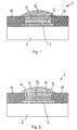
- a reference electrode designated as 1 for electrochemical A substrate 2 made of a semiconductor material has measurements or a dielectric material.
- a palladium electrode part 3 is arranged, which by a thin layer of metallic palladium is formed.
- the Palladium electrode part 3 is covered by a layer 4, those from a palladium compound which is sparingly soluble in aqueous media according to claim 1.
- a reference electrolyte adjacent to the sparingly soluble layer 4 a reference electrolyte adjacent to the sparingly soluble layer 4 5, the anions of the palladium compound of layer 4 in contains dissolved form.
- the poorly soluble layer 4 facing away side of the reference electrolyte 5 to investigating analyte 6 on the reference electrolyte 5.
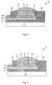
- the substrate 1 is a silicon semiconductor chip, on the surface of which a passivation layer 7 is arranged, which for example can have a silicon dioxide layer or a silicon nitride layer applied by means of CVD (chemical vapor deposition).
- the semiconductor chip also has interconnects 9, which can be prepared, for example, from poly-silicon using thin-film technology.
- the palladium electrode part 3 is also applied to a poly-silicon interconnect 9 at the intended location by means of thin-film technology. The shape and size of the palladium electrode part 3 can be selected within wide limits.
- a passivation layer 7 which for example can have a silicon dioxide layer or a silicon nitride layer applied by means of CVD (chemical vapor deposition).
- the semiconductor chip also has interconnects 9, which can be prepared, for example, from poly-silicon using thin-film technology.
- the palladium electrode part 3 is also applied to a poly-silicon interconnect 9 at the intended location by means of thin-film technology. The shape and size of the
- the palladium electrode part 3 has the shape of a circular ring segment with an area of 0.16 mm 2 .
- the poly-silicon interconnect 9 establishes the electrical connection of the palladium electrode part 3 to a palladium-coated bond point 10, which enables contact to be made with the outside.
- the palladium electrode part 3 is laterally from an insulation layer 11, which borders the palladium electrode part 3 covered at least in some areas.
- the insulation layer 11 has an interruption or cut-out on a defined area exposes the palladium electrode part 3.
- the insulation layer 11 can, for example, a structured CVD oxide layer his. This forms during the manufacture of the reference electrode 1 the carrier for the further construction of the reference electrode 1.
- a layer 4 of palladium iodide PdJ 2 which is largely insoluble in an aqueous medium, is located on the palladium electrode part 3, which layer is coated against a potential of 700 mV, for example by electrochemical iodination in 0.1 M KJ solution saturated Ag / AgCl electrode can be generated.
- an intermediate layer of finely divided palladium is arranged on the palladium layer 3.
- the palladium bath can contain, for example, 5 to 10 g / l palladium chloride, 15 to 20 g / l sodium nitrite, 40 to 50 g / l sodium chloride and 25 to 30 g / l boric acid.
- the PdJ 2 layer 4 thus produced is covered with the reference electrolyte 5 containing the anions of the palladium compound contained in the layer 4.
- the reference electrolyte 5 can be, for example, a solution which contains 0.1 M hydroiodic acid HJ.
- the reference electrolyte 5 can accordingly Figures 1 and 3 also a hydrogel formed from 2 g HEMA, 60 mg Tetraethylene glycol methacrylate, 80 mg dimethoxyphenylacetophenone, 12 mg of poly-N-vinylpyrrolidone, be that by UV radiation is networked.
- There is an electrolyte in the hydrogel for example from a mixture of water and ethylene glycol can exist in a ratio of 1: 9, the sodium bicarbonate, Sodium carbonate and potassium iodide each in the concentration Contains 0.1 mo / l.
- the contact of the PdJ 2 layer 4 with the electrolyte 5 formed by the solution or the gel forms a constant potential, the reference potential.
- This reference potential depends on the concentration of the anion (eg iodide) of the palladium compound in the reference electrolyte 5 or gel.
- the layer 4 which has the poorly soluble palladium compound according to claim 1 can, in the exemplary embodiments shown in the drawing, also electrolessly on the surface of the palladium electrode part 3 from an alcoholic iodine solution which contains 1 g of iodine in 10 ml of ethanol at 50 ° C. be deposited.
- layer 4 is also chemically deposited on palladium electrode part 3 from an aqueous solution of palladium chloride PdCl 2 and hydroiodic acid Hg.
- the Reference electrode 1 according to the invention in thick film technology executed.
- the non-conductive substrate 2 is a commercially available one Glass fiber reinforced epoxy resin hard fabric or a ceramic plate.
- the insulation layer 11 used for encapsulation consists of a polymeric insulation paste applied by screen printing.
- Layer 4 with the sparingly soluble Palladium compound according to claim 1 is according to the embodiment of Figure 3 and 4 electrolytically deposited or in the thick film process applied as a thick-film paste filled with palladium iodide.
- the reference electrolyte 5 corresponds to that of the exemplary embodiment according to FIGS. 3 and 4.
- FIG. 1 and 3 An advantageous application of the reference system according to the invention as reference electrode for amperometric measurements is shown in Fig. 1 and 3.
- the reference electrode consisting of substrate 2, the palladium electrode part 3, the Layer 4 of the insoluble palladium compound and the Reference electrolyte 5, which can be a gel, for example, in Contact with the analyte to be examined 6.
- the insulation layer 11 seals the palladium electrode part 3, the layer 4 and the reference electrolyte 5 towards the analyte 6, that only a limited area of the reference electrolyte 5 in the open Connection to analyte 6 is established.
- Reference electrode 1 at least one more Electrode, namely a measuring or working electrode 12, the the reference electrode 1 is connected to a measuring circuit.
- the Reference electrode 1 can be used as a reference electrode in this measuring circuit also act as a counter electrode.
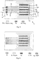
- Figure 5 shows an embodiment in which a plurality of working electrodes 12 together with two reference electrodes 1 on one common substrate are arranged.
- the working electrodes 12 and / or the bond pads 10 also consist of palladium, so that the whole in figure 5 shown measuring arrangement with methods of semiconductor technology in a simple way with only a few, in semiconductor technology preferably used substances can be produced.
- the Production of the measuring arrangement in planar technology therefore only has to comparatively few masks on or on the substrate structures or layers already present can be applied.
- FIG. 6 shows one of the prior art known measuring arrangement shown. It can be clearly seen that this measuring arrangement has significantly more substances than that of Figure 5. The manufacture of the known Measuring arrangement is therefore comparatively complicated and expensive.
- FIGS. 1 and 3 schematically show a reference electrode 1 for potentiometric measurements.
- a membrane or cover layer 13 which between the analyte 6 and the reference electrolyte 5 is arranged and this electrically insulating and separated from the analyte 6 in a liquid-tight manner.
- the top layer 13 is perforated only at a relatively small point and even closed at this point by a diaphragm 14.
- the diaphragm 14 is permeable to liquids and thus ensures the electrolytic contact of the anion in the layer 4 existing palladium compounds contain reference electrolyte 5, which can be a gel or a solution, for example the analyte 5.
- the diaphragm can be, for example, a ceramic pen or be a porous polymer membrane.
Description
- Fig. 1
- einen Querschnitt durch eine Referenzelektrode für amperometrische Messungen,
- Fig. 2
- einen Querschnitt durch eine Referenzelektrode für potentiometrische Messungen,
- Fig. 3
- einen Querschnitt durch die in Figur 5 dargestellte Referenzelektrode für amperometrische Messungen entlang der in Figur 5 mit I bezeichneten Querschnittsebene,
- Fig. 4
- eine Darstellung ähnlich Figur 2, wobei jedoch die Referenzelektrode in einen Halbleiterchip integriert ist und
- Fig. 5
- eine Aufsicht auf eine Referenzelektrode für amperometrische Messungen, wobei die Referenzelektrode in einen Halbleiterchip integriert ist und wobei der Bezugselektrolyt und die Deckschicht transparent dargestellt sind.
Claims (12)
- Referenzelektrode (1) für elektrochemische Messungen, dadurch gekennzeichnet, daß sie ein metallisches Palladium aufweisendes Elektrodenteil (3) hat, daß dieses Elektrodenteil (3) von einer Schicht (4) überdeckt ist, die in wäßrigen Medien schwerlösliches Palladiumjodid, Palladiumbromid und/oder Palladiumacetat enthält, und daß sich darüber ein Bezugselektrolyt (5) befindet, der Anionen dieser Palladiumverbindung oder Palladiumverbindungen in gelöster Form enthält.
- Referenzelektrode nach Anspruch 1, dadurch gekennzeichnet, daß das Palladium-Elektrodenteil (3) als Schicht ausgebildet ist, die auf einem Substrat (2) aus einem Halbleitermaterial angeordnet ist, und daß das Elektrodenteil (3) insbesondere in einem halbleitertechnologischen Fertigungsprozeß auf das Substrat (2) aufgebracht ist.
- Referenzelektrode nach Anspruch 1, dadurch gekennzeichnet, daß das Palladium-Elektrodenteil (3) als Schicht ausgebildet ist, die auf einem Substrat (2) aus Keramik, Glas, Glaskeramik, Leiterplattenmaterial, Polymerwerkstoff oder dergleichen dielektrischem Material besteht und die insbesondere mittels Dickschichttechnik auf das Substrat (2) aufgebracht ist.
- Referenzelektrode nach den Anspruch 3, dadurch gekennzeichnet, daß das Elektrodenteil (3) metallisches Palladium enthält, das in feinvertellter Form in ein Bindemittel aus Polymermaterial oder Cermet eingebettet ist.
- Referenzelektrode nach einem der Ansprüche 1 bis 4, dadurch gekennzeichnet, daß die das Palladiumjodid, Palladiumbromid und/oder Palladiumacetat aufweisende Schicht (4) elektrolytisch und/oder durch einen chemischen Ausfällungsprozeß in situ auf dem Palladium-Elektrodenteil (3) erzeugt ist.
- Referenzelektrode nach einem der Ansprüche 1 bis 5, dadurch gekennzeichnet, daß Anionen des Palladiumjodids, Palladiumbromids und/oder Palladiumacetats der Schicht (4) in einer ionogenen Lösung und/oder einem verfestigten Gel enthalten sind.
- Referenzelektrode nach einem der Ansprüche 1 bis 6, dadurch gekennzeichnet, daß sie auf einem Halbleiterchip oder in einem hybrid aufgebauten Mikrosystem integriert ist.
- Referenzelektrode nach einem der Ansprüche 1 bis 7, dadurch gekennzeichnet, daß das Elektrodenteil (3) und/oder die Schicht (4) ring- oder scheibenförmig ausgebildet ist, oder eine rechteckige Gestalt aufweist.
- Referenzelektrode nach einem der Ansprüche 1 bis 8, dadurch gekennzeichnet, daß sie. Teil eines elektrochemischen Meßsystems mit wenigstengs einer auf dem Substrat (2) befindlichen, insbesondere aus palladium bestehenden Arbeitselektrode (12) und/oder einem ionensensitiven Feldeffekttransistors ist, und daß die Arbeitselektrode (12) und/oder der Feldeffekttransistor vorzugsweise an der dem Palladium-Elektrodenteil (3) abgewandten Vorderseite des Substrats (2) angeordnet ist.
- Referenzelektrode nach einem der Ansprüche 1 bis 9, dadurch gekennzeichnet, daß auf dem Substrat (2) wenigstens ein Temperatursensor angeordnet ist.
- Referenzelektrode nach einem der Ansprüche 1 bis 10, dadurch gekennzeichnet, daß der die Anionen der Palladiumverbindung in gelöster Form enthaltende Bezugselektrolyt (5) mit einer nur an einer Stelle perforierten Membran oder Deckschicht (13) überzogen und eben diese Stelle mit einem für elektrochemische Messungen üblichen Diaphragma (14), zum Beispiel mittels einer porösen Membran oder einer Kationenaustauschermembran, geschlossen, jedoch für eine elektrolytische Verbindung durchgängig ist.
- Verwendung einer Referenzelektrode nach einem der Ansprüche 1 bis 11 zur Festlegung eines Bezugspotentials in einem amperometrischen und/oder potentiometrischen Meßkreis.
Applications Claiming Priority (3)
| Application Number | Priority Date | Filing Date | Title |
|---|---|---|---|
| DE19810098 | 1998-03-10 | ||
| DE19810098 | 1998-03-10 | ||
| PCT/EP1999/001369 WO1999046586A1 (de) | 1998-03-10 | 1999-03-03 | Referenzelektrode |
Publications (2)
| Publication Number | Publication Date |
|---|---|
| EP1062501A1 EP1062501A1 (de) | 2000-12-27 |
| EP1062501B1 true EP1062501B1 (de) | 2004-04-21 |
Family
ID=7860246
Family Applications (1)
| Application Number | Title | Priority Date | Filing Date |
|---|---|---|---|
| EP99911731A Expired - Lifetime EP1062501B1 (de) | 1998-03-10 | 1999-03-03 | Referenzelektrode |
Country Status (5)
| Country | Link |
|---|---|
| US (1) | US6572748B1 (de) |
| EP (1) | EP1062501B1 (de) |
| JP (1) | JP4312379B2 (de) |
| DE (1) | DE59909242D1 (de) |
| WO (1) | WO1999046586A1 (de) |
Cited By (1)
| Publication number | Priority date | Publication date | Assignee | Title |
|---|---|---|---|---|
| DE102012111811A1 (de) * | 2012-12-05 | 2014-06-05 | Endress + Hauser Conducta Gesellschaft für Mess- und Regeltechnik mbH + Co. KG | Elektrochemischer Sensor zur Erfassung einer Analytkonzentration in einem Messmedium |
Families Citing this family (32)
| Publication number | Priority date | Publication date | Assignee | Title |
|---|---|---|---|---|
| DE50015505D1 (de) * | 2000-02-10 | 2009-02-12 | Hamilton Bonaduz Ag | Polymerelektrolyt |
| EP1491519A1 (de) * | 2003-06-25 | 2004-12-29 | Mettler-Toledo GmbH | Verfahren zur Behandlung einer porösen Keramik |
| US7241500B2 (en) * | 2003-10-06 | 2007-07-10 | Certainteed Corporation | Colored roofing granules with increased solar heat reflectance, solar heat-reflective shingles, and process for producing same |
| JP4637914B2 (ja) * | 2004-11-26 | 2011-02-23 | ミクロナス ゲーエムベーハー | 電気的構成部材 |
| FR2884111B1 (fr) | 2005-04-07 | 2007-05-18 | Saint Gobain Mat Constr Sas | Granule biocide, notamment pour la fabrication de bardeau d'asphalte |
| US20070038275A1 (en) * | 2005-07-05 | 2007-02-15 | Hee-Je Kim | High-frequency electrotherapy apparatus |
| JP2007046914A (ja) * | 2005-08-05 | 2007-02-22 | Denso Corp | 油の酸性、塩基性度検出用基準電極 |
| JP4623374B2 (ja) * | 2005-08-26 | 2011-02-02 | 国立大学法人九州大学 | 化学感覚能センサチップ |
| JP4758752B2 (ja) * | 2005-12-16 | 2011-08-31 | 日本電信電話株式会社 | pH電極 |
| US7586173B2 (en) | 2006-02-27 | 2009-09-08 | Edwards Lifesciences Corporation | Method and apparatus for using flex circuit technology to create a reference electrode channel |
| US20100305420A1 (en) * | 2006-02-27 | 2010-12-02 | Edwards Lifesciences Corporation | Flexible circuit and method for forming the same |
| US7749593B2 (en) * | 2006-07-07 | 2010-07-06 | Certainteed Corporation | Solar heat responsive exterior surface covering |
| DE102006047928A1 (de) * | 2006-10-10 | 2008-04-17 | Robert Bosch Gmbh | Verfahren zur Herstellung mindestens einer porösen Schicht |
| US20100203336A1 (en) * | 2007-05-24 | 2010-08-12 | Ming Liang Shiao | Roofing granules with high solar reflectance, roofing products with high solar reflectance, and processes for preparing same |
| US8000918B2 (en) * | 2007-10-23 | 2011-08-16 | Edwards Lifesciences Corporation | Monitoring and compensating for temperature-related error in an electrochemical sensor |
| FR2923078B1 (fr) * | 2007-10-26 | 2017-09-01 | Centre Nat De La Rech Scient - Cnrs | Procede de fabrication d'un element d'interconnexion mecanique conducteur d'electricite. |
| CN101910832A (zh) * | 2007-11-02 | 2010-12-08 | 爱德华兹生命科学公司 | 具有用于系统转移或主要电源缺失的备用电源的分析物监测系统 |
| US20090188811A1 (en) * | 2007-11-28 | 2009-07-30 | Edwards Lifesciences Corporation | Preparation and maintenance of sensors |
| US8491985B2 (en) * | 2008-03-31 | 2013-07-23 | Certainteed Corporation | Coating compositions for roofing granules, dark colored roofing granules with increased solar heat reflectance, solar heat-reflective shingles, and process for producing the same |
| US20090294284A1 (en) * | 2008-05-28 | 2009-12-03 | Chung Yuan Christian University | Reference electrode |
| WO2010001277A1 (en) * | 2008-06-30 | 2010-01-07 | Nxp B.V. | Chip integrated ion sensor |
| US8900431B2 (en) | 2008-08-27 | 2014-12-02 | Edwards Lifesciences Corporation | Analyte sensor |
| EP2241882A1 (de) * | 2009-04-15 | 2010-10-20 | Neroxis SA | Elektrochemischer amperometrischer Sensor und sein Herstellungsverfahren |
| US8119869B2 (en) * | 2009-07-17 | 2012-02-21 | Monsanto Technology Llc | Soybean variety A1016276 |
| US8342007B2 (en) | 2010-02-10 | 2013-01-01 | Dionex Corporation | Electrochemical detection cell for liquid chromatography system |
| US8636885B2 (en) * | 2010-02-26 | 2014-01-28 | Dionex Corporation | Analytic device with photovoltaic power source |
| US8833146B2 (en) | 2010-04-26 | 2014-09-16 | Southwest Research Institute | Corrosion sensor |
| US20150198518A1 (en) * | 2014-01-16 | 2015-07-16 | Frank William Borin | Cathodic protection reference cell article and method |
| US10705002B2 (en) * | 2014-12-23 | 2020-07-07 | Heraeus Nexensos Gmbh | Sensor for detecting electrically conductive and/or polarizable particles and method for adjusting such a sensor |
| US10161897B2 (en) * | 2015-01-09 | 2018-12-25 | Xerox Corporation | Sensors incorporating palladium electrodes |
| US10730799B2 (en) | 2016-12-31 | 2020-08-04 | Certainteed Corporation | Solar reflective composite granules and method of making solar reflective composite granules |
| WO2022271741A1 (en) * | 2021-06-21 | 2022-12-29 | Arizona Board Of Regents On Behalf Of The University Of Arizona | Palladium-hydrogen ph electrode |
Family Cites Families (12)
| Publication number | Priority date | Publication date | Assignee | Title |
|---|---|---|---|---|
| IT1158856B (it) | 1978-06-16 | 1987-02-25 | Sclavo Inst Sieroterapeut | Sistema elettrodico con elettrodo di riferimento senza giunzione liquida per misure voltammetriche |
| US4404065A (en) * | 1980-01-14 | 1983-09-13 | Enviromental Sciences Associates, Inc. | Electrochemical detection system and method of analysis |
| GB2078962A (en) | 1980-06-11 | 1982-01-13 | Goffee Randal Antonio | Metal hydride reference electrode |
| US4536274A (en) | 1983-04-18 | 1985-08-20 | Diamond Shamrock Chemicals Company | pH and CO2 sensing device and method of making the same |
| CA1285614C (en) * | 1986-11-13 | 1991-07-02 | John E. Heider | Solid state reference electrode |
| US4933048A (en) * | 1988-02-16 | 1990-06-12 | I-Stat Corporation | Reference electrode, method of making and method of using same |
| US5368706A (en) * | 1990-03-02 | 1994-11-29 | Esa, Inc. | Amperometric detection cell |
| CA2034734A1 (en) * | 1990-03-02 | 1991-09-03 | Mark L. Bowers | Amperometric detection cell |
| EP0651248B1 (de) * | 1993-11-02 | 2001-01-24 | Siemens Plc | Vorrichtung zum Messen der Wasserqualität |
| US5702575A (en) | 1995-01-27 | 1997-12-30 | Chiron Diagnostics Corporation | Method of preparing an electrochemical planar metal/metal oxide electrode |
| DE19536901A1 (de) | 1995-10-04 | 1997-04-10 | Microparts Gmbh | Verfahren zum Herstellen integrierter Elektroden in Kunststoff-Formen, Kunststoff-Formen mit integrierten Elektroden und deren Verwendung |
| DE19641777C2 (de) | 1996-10-10 | 2001-09-27 | Micronas Gmbh | Verfahren zum Herstellen eines Sensors mit einer Metallelektrode in einer MOS-Anordnung |
-
1999
- 1999-03-03 DE DE59909242T patent/DE59909242D1/de not_active Expired - Lifetime
- 1999-03-03 EP EP99911731A patent/EP1062501B1/de not_active Expired - Lifetime
- 1999-03-03 US US09/623,839 patent/US6572748B1/en not_active Expired - Fee Related
- 1999-03-03 JP JP2000535918A patent/JP4312379B2/ja not_active Expired - Fee Related
- 1999-03-03 WO PCT/EP1999/001369 patent/WO1999046586A1/de active IP Right Grant
Cited By (1)
| Publication number | Priority date | Publication date | Assignee | Title |
|---|---|---|---|---|
| DE102012111811A1 (de) * | 2012-12-05 | 2014-06-05 | Endress + Hauser Conducta Gesellschaft für Mess- und Regeltechnik mbH + Co. KG | Elektrochemischer Sensor zur Erfassung einer Analytkonzentration in einem Messmedium |
Also Published As
| Publication number | Publication date |
|---|---|
| JP4312379B2 (ja) | 2009-08-12 |
| US6572748B1 (en) | 2003-06-03 |
| JP2003515097A (ja) | 2003-04-22 |
| DE59909242D1 (de) | 2004-05-27 |
| WO1999046586A1 (de) | 1999-09-16 |
| EP1062501A1 (de) | 2000-12-27 |
Similar Documents
| Publication | Publication Date | Title |
|---|---|---|
| EP1062501B1 (de) | Referenzelektrode | |
| DE102015121364A1 (de) | Potentiometrischer Sensor | |
| DE2820474C2 (de) | Elektrochemischer Meßfühler | |
| DE102011089671A1 (de) | Referenzhalbzelle und elektrochemischer Sensor mit der Referenzhalbzelle | |
| DE2548402A1 (de) | Multifunktioneller elektrochemischer miniatursensor fuer gleichzeitige co tief 2 -/ph-messungen | |
| DE2722617A1 (de) | Ionenselektive elektrode, verfahren zu deren herstellung und verwendung derselben | |
| DE69333218T2 (de) | Referenzelektrode | |
| EP0382831B1 (de) | Chemosensitiver wandler | |
| DE3247575C2 (de) | ||
| DE69737627T2 (de) | Analysezelle | |
| DE19714474C2 (de) | Elektrochemischer Sensor und Verfahren zu seiner Herstellung | |
| EP0597203A2 (de) | Referenzelektrode | |
| DE102017200952A1 (de) | Halbleitervorrichtung und Verfahren zur Herstellung einer Halbleitervorrichtung | |
| DE4337418C2 (de) | Verfahren zur Herstellung eines Biosensorelementes in Silizium-Technologie in einem Full-Wafer-Prozeß | |
| DE19631530C2 (de) | Ionenselektiver Sensor | |
| DE3020068C2 (de) | Chemisch empfindliche Meßzelle | |
| EP0780685A1 (de) | Amperometrischer Zweielektrodensensor, insbesondere für Wasserstoffperoxid | |
| DE4232729C2 (de) | Mikrobezugselektrode zur Erzeugung eines konstanten Bezugs- oder Referenzpotentials | |
| DE2706942A1 (de) | Kombinationselektrode | |
| DE102020121688A1 (de) | Verfahren zum Herstellen eines Sensorelements und ionenselektive Elektrode | |
| DE4302323C2 (de) | Langlebige miniaturisierbare Referenzelektrode | |
| DE3521741A1 (de) | Verfahren zur herstellung einer fluoridsensitiven membran | |
| DE4302322C2 (de) | Langlebige miniaturisierbare Referenzelektrode | |
| DE3240239A1 (de) | Ionenselektive elektrode | |
| DE3050094C2 (de) | Chemisch empfindliche Messzelle |
Legal Events
| Date | Code | Title | Description |
|---|---|---|---|
| PUAI | Public reference made under article 153(3) epc to a published international application that has entered the european phase |
Free format text: ORIGINAL CODE: 0009012 |
|
| 17P | Request for examination filed |
Effective date: 20000923 |
|
| AK | Designated contracting states |
Kind code of ref document: A1 Designated state(s): CH DE FR GB IT LI NL |
|
| GRAP | Despatch of communication of intention to grant a patent |
Free format text: ORIGINAL CODE: EPIDOSNIGR1 |
|
| GRAS | Grant fee paid |
Free format text: ORIGINAL CODE: EPIDOSNIGR3 |
|
| GRAA | (expected) grant |
Free format text: ORIGINAL CODE: 0009210 |
|
| AK | Designated contracting states |
Kind code of ref document: B1 Designated state(s): CH DE FR GB IT LI NL |
|
| REG | Reference to a national code |
Ref country code: GB Ref legal event code: FG4D Free format text: NOT ENGLISH |
|
| REG | Reference to a national code |
Ref country code: CH Ref legal event code: EP |
|
| GBT | Gb: translation of ep patent filed (gb section 77(6)(a)/1977) |
Effective date: 20040421 |
|
| REF | Corresponds to: |
Ref document number: 59909242 Country of ref document: DE Date of ref document: 20040527 Kind code of ref document: P |
|
| REG | Reference to a national code |
Ref country code: CH Ref legal event code: NV Representative=s name: R. A. EGLI & CO. PATENTANWAELTE |
|
| ET | Fr: translation filed | ||
| PLBE | No opposition filed within time limit |
Free format text: ORIGINAL CODE: 0009261 |
|
| STAA | Information on the status of an ep patent application or granted ep patent |
Free format text: STATUS: NO OPPOSITION FILED WITHIN TIME LIMIT |
|
| 26N | No opposition filed |
Effective date: 20050124 |
|
| PGFP | Annual fee paid to national office [announced via postgrant information from national office to epo] |
Ref country code: CH Payment date: 20100325 Year of fee payment: 12 |
|
| PGFP | Annual fee paid to national office [announced via postgrant information from national office to epo] |
Ref country code: FR Payment date: 20100402 Year of fee payment: 12 |
|
| PGFP | Annual fee paid to national office [announced via postgrant information from national office to epo] |
Ref country code: GB Payment date: 20100322 Year of fee payment: 12 |
|
| PGFP | Annual fee paid to national office [announced via postgrant information from national office to epo] |
Ref country code: NL Payment date: 20100315 Year of fee payment: 12 Ref country code: IT Payment date: 20100329 Year of fee payment: 12 Ref country code: DE Payment date: 20100324 Year of fee payment: 12 |
|
| REG | Reference to a national code |
Ref country code: NL Ref legal event code: V1 Effective date: 20111001 |
|
| REG | Reference to a national code |
Ref country code: CH Ref legal event code: PL |
|
| GBPC | Gb: european patent ceased through non-payment of renewal fee |
Effective date: 20110303 |
|
| REG | Reference to a national code |
Ref country code: FR Ref legal event code: ST Effective date: 20111130 |
|
| PG25 | Lapsed in a contracting state [announced via postgrant information from national office to epo] |
Ref country code: DE Free format text: LAPSE BECAUSE OF NON-PAYMENT OF DUE FEES Effective date: 20111001 Ref country code: FR Free format text: LAPSE BECAUSE OF NON-PAYMENT OF DUE FEES Effective date: 20110331 Ref country code: CH Free format text: LAPSE BECAUSE OF NON-PAYMENT OF DUE FEES Effective date: 20110331 Ref country code: NL Free format text: LAPSE BECAUSE OF NON-PAYMENT OF DUE FEES Effective date: 20111001 Ref country code: LI Free format text: LAPSE BECAUSE OF NON-PAYMENT OF DUE FEES Effective date: 20110331 |
|
| REG | Reference to a national code |
Ref country code: DE Ref legal event code: R119 Ref document number: 59909242 Country of ref document: DE Effective date: 20111001 |
|
| PG25 | Lapsed in a contracting state [announced via postgrant information from national office to epo] |
Ref country code: GB Free format text: LAPSE BECAUSE OF NON-PAYMENT OF DUE FEES Effective date: 20110303 Ref country code: IT Free format text: LAPSE BECAUSE OF NON-PAYMENT OF DUE FEES Effective date: 20110303 |