EP1062501B1 - Reference electrode - Google Patents
Reference electrode Download PDFInfo
- Publication number
- EP1062501B1 EP1062501B1 EP99911731A EP99911731A EP1062501B1 EP 1062501 B1 EP1062501 B1 EP 1062501B1 EP 99911731 A EP99911731 A EP 99911731A EP 99911731 A EP99911731 A EP 99911731A EP 1062501 B1 EP1062501 B1 EP 1062501B1
- Authority
- EP
- European Patent Office
- Prior art keywords
- palladium
- reference electrode
- layer
- electrode
- substrate
- Prior art date
- Legal status (The legal status is an assumption and is not a legal conclusion. Google has not performed a legal analysis and makes no representation as to the accuracy of the status listed.)
- Expired - Lifetime
Links
Images
Classifications
-
- G—PHYSICS
- G01—MEASURING; TESTING
- G01N—INVESTIGATING OR ANALYSING MATERIALS BY DETERMINING THEIR CHEMICAL OR PHYSICAL PROPERTIES
- G01N27/00—Investigating or analysing materials by the use of electric, electrochemical, or magnetic means
- G01N27/26—Investigating or analysing materials by the use of electric, electrochemical, or magnetic means by investigating electrochemical variables; by using electrolysis or electrophoresis
- G01N27/28—Electrolytic cell components
- G01N27/30—Electrodes, e.g. test electrodes; Half-cells
- G01N27/301—Reference electrodes
Definitions
- the invention relates to a reference electrode for electrochemical Measurements.
- Reference electrodes in electrochemical measuring circuits as an electrical reference point in a medium to be examined provided.
- Reference electrodes are reversible, non-polarizable Half cells that are as constant as possible from the components largely independent of the medium to be examined Develop potential.
- the primary reference electrode in electrochemical measurement technology is the standard hydrogen electrode, the potential of which by definition is set to zero at all temperatures.
- electrodes of the second type are used almost exclusively as reference electrodes, since these are easier to handle. They essentially consist of a metal which is coated with a layer of a poorly soluble compound of this metal and immersed in a solution which contains a soluble compound with the anion present in the layer [F. Oehme: Ion-selective electrodes, Dr. Alfred Wilsonhig Verlag, Heidelberg 1986, p. 67].
- the most widespread are reference electrodes of the Ag / AgCl, Cl, and Hg / Hg 2 Cl type.
- the electrode part can then in an electrochemical measuring circuit be assigned a working electrode made of palladium, so that Reference and working electrode made of the same metallic Starting material can be manufactured.
- the electrode part of the reference electrode is a palladium wire be with a compound that is sparingly soluble in aqueous media of palladium according to claim 1, is coated and in an aqueous or gel-like medium dips, the anions of the palladium compound contains.
- An uncoated electrode can then be used as the working electrode Palladium wire can be provided.
- the reference electrode according to the invention largely insensitive to light is. An opaque shielding of the This eliminates the need for a reference electrode.
- the sensor has a measuring electrode with an electrode part made of metallic palladium, which is covered by a layer of palladium oxide.
- the CO 2 content is determined indirectly by measuring the pH by means of the measuring electrode.
- the measuring electrode is assigned a silver / silver chloride electrode as a reference electrode.
- the electrical potential at the palladium / palladium oxide electrode changes as a function of the pH of the electrolyte in contact with the electrode, while the potential of the reference electrode remains constant regardless of the pH.
- the palladium electrode part is formed as a layer that is arranged on a substrate made of a semiconductor material, the electrode part in particular in a semiconductor technology Manufacturing process applied to the substrate is.
- the reference electrode can then have particularly small dimensions exhibit.
- additional structures in the substrate be applied or applied to this, for example Structures for an evaluation device for processing a Measuring signals, a working electrode, a sensor and / or like components. It can be used to manufacture the Palladium electrode part on the substrate or on it located layer (s) applied metallization at the same time to form a palladium structure for an additional component can be used. That too Poorly soluble layer containing palladium salt according to claim 1 can be very effective and inexpensive to apply, because on one Wafers a large number of electrode structures can be located that are prepared simultaneously in one production step can.
- the palladium electrode part can be particularly advantageous applied by means of the method known from DE 196 41 777 A1 become.
- a structure for the Palladium electrode part produced from a material with predetermined adhesive properties for metallic palladium exists, and then a palladium metallization of the Surface of the arrangement comprising the structure, where the palladium metallization is only on the structure for the palladium electrode part sticks. That way the palladium electrode part without the use of an additional one photolithographic paint mask on the substrate or the structure on it can be applied.
- This is in particular, it is possible for the manufacture of the reference electrode required process steps in a CMOS process integrate.
- the palladium electrode part formed as a layer on a substrate made of ceramic, glass, glass ceramic, circuit board material, polymer material or the like dielectric material and which in particular by means of thick film technology on the substrate is applied.
- the reference electrode is then special inexpensive to produce, for example by means of sieve or Screen printing.
- the electrode part is metallic palladium contains that in a finely divided form into a binder Polymer material or cermet is embedded.
- the palladium in a pasty or liquid medium, for example by means of screen printing or Stencil printing can be applied to the substrate. The medium can then be cured, dried or solidified become.
- the poorly soluble palladium compound contains palladium iodide, palladium bromide and / or palladium acetate.
- the palladium compound is then simple using electrochemical processes and inexpensive to manufacture. It is even possible that this poorly soluble layer electrolytically and / or by a chemical precipitation process deposited or generated in situ on the palladium electrode part is.
- the Anions of the poorly soluble palladium compound according to claim 1 in an ionogenic Contain solution and / or a solidified gel You can the ion-containing solution and / or the solidified gel, if appropriate between an ion permeable membrane and the metallic one Palladium layer may be included.
- Reference electrode on a semiconductor chip or in a hybrid built microsystem integrated can For example, have a carrier on which the reference electrode and other components such as an evaluation device and / or an ion-selective working electrode could be.
- the individual components can be selected using known micro-technological processes on the carrier be mounted. Overall, this results in a compact assembled measuring device.
- the electrode part and / or that which is sparingly soluble in aqueous media Palladium compound layer according to claim 1 can ring or be disc-shaped or a rectangular shape exhibit.
- the application of the invention is not to a planar Reference electrode limited.
- a cylindrical reference electrode can be created by a palladium wire which is difficult to dissolve in aqueous media
- Compound of the palladium according to claim 1 is coated in a aqueous or gel medium immerses the anions of the Contains palladium compound.
- the reference electrode is a part an electrochemical measuring system with at least one on the Substrate located, especially made of palladium Working electrode and / or an ion-sensitive field effect transistor is, and that the working electrode and / or or Field effect transistor preferably on the palladium electrode part facing away from the front of the substrate is arranged.
- the electrochemical reference system is then special inexpensive to manufacture.
- At least one temperature sensor is expediently on the substrate arranged. A possible influence of the Ambient temperature and or the temperature of the to be examined Medium to the reference potential of the reference electrode can then compensated or taken into account in some other way.
- the reference system according to the invention is preferably a reference electrode used in an amperometric sensor.
- a reference electrode used in an amperometric sensor.
- the membrane is preferred chemically inert, electrically insulating and / or liquid-tight educated.
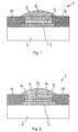
- a reference electrode designated as 1 for electrochemical A substrate 2 made of a semiconductor material has measurements or a dielectric material.
- a palladium electrode part 3 is arranged, which by a thin layer of metallic palladium is formed.
- the Palladium electrode part 3 is covered by a layer 4, those from a palladium compound which is sparingly soluble in aqueous media according to claim 1.
- a reference electrolyte adjacent to the sparingly soluble layer 4 a reference electrolyte adjacent to the sparingly soluble layer 4 5, the anions of the palladium compound of layer 4 in contains dissolved form.
- the poorly soluble layer 4 facing away side of the reference electrolyte 5 to investigating analyte 6 on the reference electrolyte 5.
- the substrate 1 is a silicon semiconductor chip, on the surface of which a passivation layer 7 is arranged, which for example can have a silicon dioxide layer or a silicon nitride layer applied by means of CVD (chemical vapor deposition).
- the semiconductor chip also has interconnects 9, which can be prepared, for example, from poly-silicon using thin-film technology.
- the palladium electrode part 3 is also applied to a poly-silicon interconnect 9 at the intended location by means of thin-film technology. The shape and size of the palladium electrode part 3 can be selected within wide limits.
- a passivation layer 7 which for example can have a silicon dioxide layer or a silicon nitride layer applied by means of CVD (chemical vapor deposition).
- the semiconductor chip also has interconnects 9, which can be prepared, for example, from poly-silicon using thin-film technology.
- the palladium electrode part 3 is also applied to a poly-silicon interconnect 9 at the intended location by means of thin-film technology. The shape and size of the
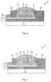
- the palladium electrode part 3 has the shape of a circular ring segment with an area of 0.16 mm 2 .
- the poly-silicon interconnect 9 establishes the electrical connection of the palladium electrode part 3 to a palladium-coated bond point 10, which enables contact to be made with the outside.
- the palladium electrode part 3 is laterally from an insulation layer 11, which borders the palladium electrode part 3 covered at least in some areas.
- the insulation layer 11 has an interruption or cut-out on a defined area exposes the palladium electrode part 3.
- the insulation layer 11 can, for example, a structured CVD oxide layer his. This forms during the manufacture of the reference electrode 1 the carrier for the further construction of the reference electrode 1.
- a layer 4 of palladium iodide PdJ 2 which is largely insoluble in an aqueous medium, is located on the palladium electrode part 3, which layer is coated against a potential of 700 mV, for example by electrochemical iodination in 0.1 M KJ solution saturated Ag / AgCl electrode can be generated.
- an intermediate layer of finely divided palladium is arranged on the palladium layer 3.
- the palladium bath can contain, for example, 5 to 10 g / l palladium chloride, 15 to 20 g / l sodium nitrite, 40 to 50 g / l sodium chloride and 25 to 30 g / l boric acid.
- the PdJ 2 layer 4 thus produced is covered with the reference electrolyte 5 containing the anions of the palladium compound contained in the layer 4.
- the reference electrolyte 5 can be, for example, a solution which contains 0.1 M hydroiodic acid HJ.
- the reference electrolyte 5 can accordingly Figures 1 and 3 also a hydrogel formed from 2 g HEMA, 60 mg Tetraethylene glycol methacrylate, 80 mg dimethoxyphenylacetophenone, 12 mg of poly-N-vinylpyrrolidone, be that by UV radiation is networked.
- There is an electrolyte in the hydrogel for example from a mixture of water and ethylene glycol can exist in a ratio of 1: 9, the sodium bicarbonate, Sodium carbonate and potassium iodide each in the concentration Contains 0.1 mo / l.
- the contact of the PdJ 2 layer 4 with the electrolyte 5 formed by the solution or the gel forms a constant potential, the reference potential.
- This reference potential depends on the concentration of the anion (eg iodide) of the palladium compound in the reference electrolyte 5 or gel.
- the layer 4 which has the poorly soluble palladium compound according to claim 1 can, in the exemplary embodiments shown in the drawing, also electrolessly on the surface of the palladium electrode part 3 from an alcoholic iodine solution which contains 1 g of iodine in 10 ml of ethanol at 50 ° C. be deposited.
- layer 4 is also chemically deposited on palladium electrode part 3 from an aqueous solution of palladium chloride PdCl 2 and hydroiodic acid Hg.
- the Reference electrode 1 according to the invention in thick film technology executed.
- the non-conductive substrate 2 is a commercially available one Glass fiber reinforced epoxy resin hard fabric or a ceramic plate.
- the insulation layer 11 used for encapsulation consists of a polymeric insulation paste applied by screen printing.
- Layer 4 with the sparingly soluble Palladium compound according to claim 1 is according to the embodiment of Figure 3 and 4 electrolytically deposited or in the thick film process applied as a thick-film paste filled with palladium iodide.
- the reference electrolyte 5 corresponds to that of the exemplary embodiment according to FIGS. 3 and 4.
- FIG. 1 and 3 An advantageous application of the reference system according to the invention as reference electrode for amperometric measurements is shown in Fig. 1 and 3.
- the reference electrode consisting of substrate 2, the palladium electrode part 3, the Layer 4 of the insoluble palladium compound and the Reference electrolyte 5, which can be a gel, for example, in Contact with the analyte to be examined 6.
- the insulation layer 11 seals the palladium electrode part 3, the layer 4 and the reference electrolyte 5 towards the analyte 6, that only a limited area of the reference electrolyte 5 in the open Connection to analyte 6 is established.
- Reference electrode 1 at least one more Electrode, namely a measuring or working electrode 12, the the reference electrode 1 is connected to a measuring circuit.
- the Reference electrode 1 can be used as a reference electrode in this measuring circuit also act as a counter electrode.
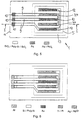
- Figure 5 shows an embodiment in which a plurality of working electrodes 12 together with two reference electrodes 1 on one common substrate are arranged.
- the working electrodes 12 and / or the bond pads 10 also consist of palladium, so that the whole in figure 5 shown measuring arrangement with methods of semiconductor technology in a simple way with only a few, in semiconductor technology preferably used substances can be produced.
- the Production of the measuring arrangement in planar technology therefore only has to comparatively few masks on or on the substrate structures or layers already present can be applied.
- FIG. 6 shows one of the prior art known measuring arrangement shown. It can be clearly seen that this measuring arrangement has significantly more substances than that of Figure 5. The manufacture of the known Measuring arrangement is therefore comparatively complicated and expensive.
- FIGS. 1 and 3 schematically show a reference electrode 1 for potentiometric measurements.
- a membrane or cover layer 13 which between the analyte 6 and the reference electrolyte 5 is arranged and this electrically insulating and separated from the analyte 6 in a liquid-tight manner.
- the top layer 13 is perforated only at a relatively small point and even closed at this point by a diaphragm 14.
- the diaphragm 14 is permeable to liquids and thus ensures the electrolytic contact of the anion in the layer 4 existing palladium compounds contain reference electrolyte 5, which can be a gel or a solution, for example the analyte 5.
- the diaphragm can be, for example, a ceramic pen or be a porous polymer membrane.
Description
Die Erfindung betrifft eine Referenzelektrode für elektrochemische Messungen.The invention relates to a reference electrode for electrochemical Measurements.
Es ist bekannt, Referenzelektroden in elektrochemischen Meßkreisen als elektrischen Bezugspunkt in einem zu untersuchenden Medium vorzusehen. Referenzelektroden sind reversible, nicht polarisierbare Halbzellen, die ein möglichst konstantes, von den Bestandteilen des zu untersuchenden Mediums weitestgehend unabhängiges Potential ausbilden.It is known to use reference electrodes in electrochemical measuring circuits as an electrical reference point in a medium to be examined provided. Reference electrodes are reversible, non-polarizable Half cells that are as constant as possible from the components largely independent of the medium to be examined Develop potential.
Die primäre Referenzelektrode in der elektrochemischen Meßtechnik ist die Standard-Wasserstoffelektrode, deren Potential definitionsgemäß bei allen Temperaturen gleich Null gesetzt wird. In der Praxis werden jedoch fast ausschließlich Elektroden 2. Art als Referenzelektroden verwendet, da diese einfacher handhabbar sind. Sie bestehen im wesentlichen aus einem Metall, das mit einer Schicht aus einer schwerlöslichen Verbindung dieses Metalls überzogen ist und in eine Lösung taucht, die eine lösliche Verbindung mit dem in der Schicht vorhandenen Anion enthält [F. Oehme: Ionenselektive Elektroden, Dr. Alfred Hüthig Verlag, Heidelberg 1986, S. 67]. Am weitesten verbreitet sind Referenzelektroden vom Typ Ag/AgCl, Cl, und Hg/Hg2Cl. Die Standardpotentiale dieser Referenzelektroden sind genau bekannt, so daß die damit gemessenen Potentiale leicht auf das Potential der Standard-Wasserstoffelektrode umgerechnet werden können [K. Schwabe Physikalische Chemie. Band 2: Elektrochemie. AkademieVerlag, Berlin 1975, 5. 177]. Da die genannten Referenzelektroden universell einsetzbar sind und hohe Potentialkonstanz aufweisen, haben andere metallische Elektrodenmaterialien in elektrochemischen Referenzelektroden neben den genannten Metallen Silber und Quecksilber nur geringe Bedeutung. The primary reference electrode in electrochemical measurement technology is the standard hydrogen electrode, the potential of which by definition is set to zero at all temperatures. In practice, however, electrodes of the second type are used almost exclusively as reference electrodes, since these are easier to handle. They essentially consist of a metal which is coated with a layer of a poorly soluble compound of this metal and immersed in a solution which contains a soluble compound with the anion present in the layer [F. Oehme: Ion-selective electrodes, Dr. Alfred Hüthig Verlag, Heidelberg 1986, p. 67]. The most widespread are reference electrodes of the Ag / AgCl, Cl, and Hg / Hg 2 Cl type. The standard potentials of these reference electrodes are precisely known, so that the potentials measured with them can easily be converted to the potential of the standard hydrogen electrode [K. Schwabe physical chemistry. Volume 2: electrochemistry. AkademieVerlag, Berlin 1975, 5. 177]. Since the reference electrodes mentioned can be used universally and have high potential constancy, other metallic electrode materials in electrochemical reference electrodes are of little importance in addition to the metals mentioned silver and mercury.
Aus Lambrechts, M. et al., Biosensors: Microelectrochemical Devices, Katholieke Universiteit Leuven, Institut of Physics Publishig, Bristol, Philadelphia and New York (1992), Seite 165 kennt man bereits eine Referenzelektrode der eingangs genannten Art, die auf einem Substrat aus Halbleitermaterial eine Schicht aus metallischem Silber und auf dieser eine Schicht aus Silberchlorid aufweist. Diese Referenzelektrode hat jedoch den Nachteil, daß das Silberchlorid lichtempfindlich ist und unter Lichteinwirkung zu metallischem Silber reduziert werden kann. Um eine Zerstörung der Referenzelektrode durch Lichteinwirkung zu vermeiden, sind deshalb geeignete Schutzmaßnahmen erforderlich. Der vorbekannten Referenzelektrode ist eine Arbeitselektrode aus Gold zugeordnet, die mit der Referenzelektrode zu einem elektrochemischen Meßkreis verbunden wird. Arbeits- und Referenzelektrode sind auf einem gemeinsamen Subs trat angeordnet. Ein Nachteil dieser Elektrodenanordnung besteht jedoch noch darin, daß die Referenz- und die Arbeitselektrode aus unterschiedlichen metallischen Materialien defertigt sind, nämlich aus Silber und Gold, was bei einer Herstellung der Referenzelektrode in Planartechnik die Aufbringung zusätzlicher lithographischen Masken erfordert.From Lambrechts, M. et al., Biosensors: Microelectrochemical Devices, Katholieke Universiteit Leuven, Institute of Physics Publishig, Bristol, Philadelphia and New York (1992), page 165 one already knows a reference electrode of the aforementioned Kind that a layer on a substrate of semiconductor material made of metallic silver and a layer on it Has silver chloride. However, this reference electrode has the Disadvantage that the silver chloride is sensitive to light and under Exposure to light can be reduced to metallic silver. To destroy the reference electrode by exposure to light To avoid this, suitable protective measures are necessary. The known reference electrode is a working electrode Gold assigned to the one with the reference electrode electrochemical measuring circuit is connected. Labor and Reference electrodes are arranged on a common subs. A disadvantage of this electrode arrangement is, however, that that the reference and the working electrode from different metallic materials are made, namely from silver and Gold, which is the result of a production of the reference electrode in Planar technology the application of additional lithographic Masks required.
Es besteht deshalb die Aufgabe, eine Referenzelektrode der eingangs genannten Art zu schaffen, bei der die vorstehend genannten Nachteile vermieden werden.There is therefore the task of a reference electrode to create the type mentioned, in which the above mentioned disadvantages can be avoided.
Die Lösung dieser Aufgabe besteht in einer Referenzelektrode
gemäß Anspruch 1. The solution to this problem is a reference electrode
according to
Dem Elektrodenteil kann dann in einem elektrochemischen Meßkreis
eine Arbeitselektrode aus Palladium zugeordnet sein, so daß
Referenz- und Arbeitselektrode aus dem gleichen metallischen
Ausgangsmaterial gefertigt werden können. So kann beispielsweise
das Elektrodenteil der Referenzelektrode ein Palladiumdraht
sein, der mit einer in wäßrigen Medien schwerlöslichen Verbindung
des Palladiums gemäß Anspruch 1, beschichtet ist und in ein wäßriges oder
gelförmiges Medium taucht, das Anionen der Palladiumverbindung
enthält. Als Arbeitselektrode kann dann ein unbeschichteter
Palladiumdraht vorgesehen sein. Vorteilhaft ist außerdem, daß
die erfindungsgemäße Referenzelektrode weitestgehend lichtunempfindlich
ist. Eine lichtundurchlässige Abschirmung der
Referenzelektrode kann dadurch entfallen.The electrode part can then in an electrochemical measuring circuit
be assigned a working electrode made of palladium, so that
Reference and working electrode made of the same metallic
Starting material can be manufactured. For example
the electrode part of the reference electrode is a palladium wire
be with a compound that is sparingly soluble in aqueous media
of palladium according to
Der Einsatz von Palladium als Sensormaterial ist zwar für einen gattungsfremden wasserstoffsensitiven Gassensor aus Lundström, I., et al., Hydrogensensitive MOS field effect transistor, Appl. Phys. Lett. 26 (1975), S. 55-67, bereits bekannt. Wenn bei einem MOS-Feldeffekttransistor das Metall auf dem Gateisolator SiO durch eine dünne Schicht (< 100 nm) Palladium ersetzt wird, so diffundieren Wasserstoffatome aus der Umgebung durch diese Schicht zur Phasengrenze Pd/SiO , wodurch sich die Austrittsarbeit in der Palladiumschicht verändert und eine meßbare Verschiebung in der Schwellspannung des Feldeffektransistors auftritt. Der vorbekannte wasserstoffsensitive Gassensor weist jedoch einen ganz anderen Aufbau als die erfindungsgemäße Referenzelektrode auf und dient nicht der Gewinnung eines Referenzpotentials.The use of palladium as a sensor material is indeed for one Non-generic hydrogen-sensitive gas sensor from Lundström, I., et al., Hydrogen sensitive MOS field effect transistor, Appl. Phys. Lett. 26 (1975), pp. 55-67, already known. If at one MOS field effect transistor the metal on the gate insulator SiO is replaced by a thin layer (<100 nm) of palladium, so hydrogen atoms diffuse from the environment through this layer to the phase boundary Pd / SiO, whereby the work function in the palladium layer changed and a measurable shift in the threshold voltage of the field effect transistor occurs. The However, known hydrogen-sensitive gas sensor has one completely different structure than the reference electrode according to the invention and does not serve to obtain a reference potential.
Es wurde auch bereits versucht, unter Verwendung von Palladium Betriebs-Wasserstoffelektroden als Elektroden erster Art für die pH-Messung in flußsäurehaltigen Beizbäderm herzustellen, die darauf beruhen, daß Palladium Wasserstoff in größerer Menge aufnehmen kann, Jasinski, R., A Palladium Hydride pH Electrode for Use in Buffered Fluoride Etoh Solutions, J. Electrochem. Soc. 121 (1974), S. 1579-1584. Die Standzeiten derartiger Elektroden sind jedoch gering. Daher haben sie bis heute keine technische Bedeutung erlangt, Galster, H., pH-Messung, VCH Verlagsgesellschaft, Weinheim (1990), S. 69; Shao, M. et al., pH measurements based on a palladium electrode, Electroanalysis 6 (1994), S. 245-249.It has also been tried using palladium Operating hydrogen electrodes as electrodes of the first kind for To produce pH measurement in hydrofluoric acid pickling baths are based on the fact that palladium is hydrogen in large quantities Jasinski, R., A Palladium Hydride pH Electrode for Use in Buffered Fluoride Etoh Solutions, J. Electrochem. Soc. 121 (1974), pp. 1579-1584. The service life of such electrodes are small, however. Therefore, to date, they have no technical Gaining importance, Galster, H., pH measurement, VCH publishing company, Weinheim (1990), p. 69; Shao, M. et al., PH measurements based on a palladium electrode, Electroanalysis 6 (1994), pp. 245-249.
Das System Palladium/Wasserstoff wird auch in US 4 404 065 als Referenzsystem in miniaturisierbarer Ausführung angegeben, z.B. für coulometrische Sensoren in Fließverfahren oder für amperometrische Sensoren in Dünnschichtausführung. Trotz des Vorteils, daß dieses Referenzsystem bis zu hohen Drücken (> 4 Mpa) verwendbar ist, wird seine Anwendbarkeit dadurch wesentlich eingeschränkt, daß eine ausgeprägte pH-Sensitivität auftritt.The palladium / hydrogen system is also described in US 4,440,065 Reference system specified in miniaturizable version, e.g. for coulometric sensors in flow processes or for amperometric Thin-film sensors. Despite the advantage that this reference system up to high pressures (> 4 Mpa) is usable, its applicability becomes essential limited that a pronounced pH sensitivity occurs.
Aus GB-A-2 023 846 ist auch bereits eine Referenzelektrode mit einem Elektrodenteil aus metallischem Palladium bekannt, das von einer Schicht aus Palladiumoxid überdeckt ist, die mit dem Bezugselektrolyt in Kontakt steht. Auch diese Referenzelektrode weist eine ausgeprägte Abhängigkeit ihres Elektrodenpotentials vom pH-Wert des Bezugselektrolyten auf.From GB-A-2 023 846 a reference electrode is already included an electrode part made of metallic palladium known from a layer of palladium oxide is covered with the Reference electrolyte is in contact. This reference electrode too shows a pronounced dependence on their electrode potential from the pH value of the reference electrolyte.
Aus US-A-4 536 274 ist auch bereits ein Sensor zur transkutanen Messung des CO2-Gehalts im Blut beschrieben. Der Sensor weist eine Meßelektrode mit einen Elektrodenteil aus metallischem Palladium auf, das von einer Schicht aus Palladiumoxid überdeckt ist. Mittels der Meßelektrcde wird der CO2-Gehalt indirekt durch Messung des pH-Wertes ermittelt. Dabei ist der Meßelektrode eine Silber/Silberchlorid-Elektrode als Referenzelektrode zugeordnet. Das elektrische Potential an der Palladium/Palladiumoxid-Elektrode ändert sich in Abhängigkeit vom pH-Wert des mit der Elektrode in Kontakt stehenden Elektrolyten, während das Potentail der Referenzelektrode unabhängig vom pH-Wert konstant bleibt. From US-A-4 536 274 a sensor for transcutaneous measurement of the CO 2 content in the blood has already been described. The sensor has a measuring electrode with an electrode part made of metallic palladium, which is covered by a layer of palladium oxide. The CO 2 content is determined indirectly by measuring the pH by means of the measuring electrode. The measuring electrode is assigned a silver / silver chloride electrode as a reference electrode. The electrical potential at the palladium / palladium oxide electrode changes as a function of the pH of the electrolyte in contact with the electrode, while the potential of the reference electrode remains constant regardless of the pH.
Bei einer besonders vorteilhaften Ausgestaltung der Erfindung
ist das Palladium-Elektrodenteil als Schicht ausgebildet, die
auf einem Substrat aus einem Halbleitermaterial angeordnet ist,
wobei das Elektrodenteil insbesondere in einem halbleitertechnologischen
Fertigungsprozeß auf das Substrat aufgebracht
ist. Die Referenzelektrode kann dann besonders kleine Abmessungen
aufweisen. Darüber hinaus können mittels des halbleitertechnologischen
Fertigungsprozesses bei der Herstellung der
Referenzelektrode auch noch zusätzliche Strukturen in das Substrat
ein- oder auf dieses aufgebracht werden, beispielsweise
Strukturen für eine Auswerteeinrichtung zur Verarbeitung eines
Meßsignales, eine Arbeitselektrode, ein Sensor und/oder
dergleichen Komponenten. Dabei kann eine zur Herstellung des
Palladium-Elektrodenteils auf das Substrat oder die darauf
befindliche(n) Schicht(en) aufgebrachte Metallisierung
gleichzeitig auch zur Ausbildung einer Palladium-Struktur für
eine zusätzliche Komponente genutzt werden. Auch die das
schwerlösliche Palladiumsalz enthaltende Schicht gemäß Anspruch 1 läßt sich
sehr effektiv und kostengünstig aufbringen, da sich auf einem
Wafer eine große Anzahl von Elektrodenstrukturen befinden können,
die in einem Fertigungsschritt gleichzeitig präpariert werden
können.In a particularly advantageous embodiment of the invention
the palladium electrode part is formed as a layer that
is arranged on a substrate made of a semiconductor material,
the electrode part in particular in a semiconductor technology
Manufacturing process applied to the substrate
is. The reference electrode can then have particularly small dimensions
exhibit. In addition, using the semiconductor technology
Manufacturing process in the manufacture of the
Reference electrode also additional structures in the substrate
be applied or applied to this, for example
Structures for an evaluation device for processing a
Measuring signals, a working electrode, a sensor and / or
like components. It can be used to manufacture the
Palladium electrode part on the substrate or on it
located layer (s) applied metallization
at the same time to form a palladium structure for
an additional component can be used. That too
Poorly soluble layer containing palladium salt according to
Das Palladium-Elektrodenteil kann besonders vorteilhaft mittels des aus DE 196 41 777 A1 bekannten Verfahrens aufgebracht werden. Dabei wird auf dem Substrat eine Struktur für das Palladium-Elektrodenteil erzeugt, die aus einem Material mit vorbestimmten Hafteigenschaften für metallisches Palladium besteht, und danach wird eine Palladium-Metallisierung der Oberfläche der die Struktur aufweisenden Anordnung vorgenommen, bei der die Palladium-Metallisierung nur auf der Struktur für das Palladium-Elektrodenteil haften bleibt. Auf diese Weise kann das Palladium-Elektrodenteil ohne die Verwendung einer zusätzl i-chen photolithografischen Lackmaske auf das Substrat bzw. die darauf befindliche Struktur aufgebracht werden. Dadurch ist es insbesondere möglich, die für die Herstellung der Referenzelektrode erforderlichen Verfahrensschritte in einen CMOS-Prozeß einzubinden.The palladium electrode part can be particularly advantageous applied by means of the method known from DE 196 41 777 A1 become. A structure for the Palladium electrode part produced from a material with predetermined adhesive properties for metallic palladium exists, and then a palladium metallization of the Surface of the arrangement comprising the structure, where the palladium metallization is only on the structure for the palladium electrode part sticks. That way the palladium electrode part without the use of an additional one photolithographic paint mask on the substrate or the structure on it can be applied. This is in particular, it is possible for the manufacture of the reference electrode required process steps in a CMOS process integrate.
Bei einer anderen Ausführungsform der Erfindung ist das Palladium-Elektrodenteil als Schicht ausgebildet, die auf einem Substrat aus Keramik, Glas, Glaskeramik, Leiterplattenmaterial, Polymerwerkstoff oder dergleichen dielektrischem Material besteht und die insbesondere mittels Dickschichttechnik auf das Substrat aufgebracht ist. Die Referenzelektrode ist dann besonders kostengünstig herstellbar, beispielsweise mittels Sieb- oder Schablonendrucks.In another embodiment of the invention, the palladium electrode part formed as a layer on a substrate made of ceramic, glass, glass ceramic, circuit board material, polymer material or the like dielectric material and which in particular by means of thick film technology on the substrate is applied. The reference electrode is then special inexpensive to produce, for example by means of sieve or Screen printing.
Vorteilhaft ist, wenn das Elektrodenteil metallisches Palladium enthält, das in feinvertellter Form in ein Bindemittel aus Polymermaterial oder Cermet eingebettet ist. Bei der Herstellung der Referenzelektrode kann das Palladium in einem pastösen oder flüssigen Medium beispielsweise mittels Siebdruck oder Schablonendruck auf das Substrat aufgebracht werden. Das Medium kann dann anschließend ausgehärtet, getrocknet oder verfestigt werden.It is advantageous if the electrode part is metallic palladium contains that in a finely divided form into a binder Polymer material or cermet is embedded. In the preparation of the reference electrode can be the palladium in a pasty or liquid medium, for example by means of screen printing or Stencil printing can be applied to the substrate. The medium can then be cured, dried or solidified become.
Die schwerlösliche Palladiumverbindung enthält Palladiumjodid, Palladiumbromid und/oder Palladiumacetat. Die Palladiumverbindung ist dann mittels elektrochemischer Verfahren einfach und kostengünstig herstellbar. Dabei ist es sogar möglich, daß diese schwerlösliche Schicht elektrolytisch und/oder durch einen chemischen Ausfällungsprozeß in situ auf dem Palladium-Elektrodenteil abgeschieden oder erzeugt ist.The poorly soluble palladium compound contains palladium iodide, palladium bromide and / or palladium acetate. The palladium compound is then simple using electrochemical processes and inexpensive to manufacture. It is even possible that this poorly soluble layer electrolytically and / or by a chemical precipitation process deposited or generated in situ on the palladium electrode part is.
Bei einer vorteilhaften Ausführungsform der Erfindung sind die
Anionender schwerlöslichen Palladiumverbindung gemäß Anspruch 1 in einer ionogenen
Lösung und/oder einem verfestigten Gel enthalten. Dabei können
die ionenhaltige Lösung und/oder das verfestigte Gel gegebenenfalls
zwischen einer ionendurchlässigen Membran und der metallischen
Palladium-Schicht eingeschlossen sein.In an advantageous embodiment of the invention, the
Anions of the poorly soluble palladium compound according to
Bei einer zweckmäßigen Ausgestaltung der Erfindung ist die Referenzelektrode auf einem Halbleiterchip oder in einem hybrid aufgebauten Mikrosystem integriert. Das Mikrosystem kann beispielsweise einen Träger aufweisen, auf dem die Referenzelektrode und weitere Komponenten, wie z.B. eine Auswerteeinrichtung und/oder eine ionenselektive Arbeitselektrode, angeordnet sein können. Dabei können die einzelnen Komponenten mittels an sich bekannter mikrotechnologischer Verfahren auf dem Träger montiert sein. Insgesamt ergibt sich dadurch eine kompakt aufgebaute Meßeinrichtung.In an expedient embodiment of the invention Reference electrode on a semiconductor chip or in a hybrid built microsystem integrated. The microsystem can For example, have a carrier on which the reference electrode and other components such as an evaluation device and / or an ion-selective working electrode could be. The individual components can be selected using known micro-technological processes on the carrier be mounted. Overall, this results in a compact assembled measuring device.
Das Elektrodenteil und/oder die die in wäßrigen Medien schwerlösliche
Palladiumverbindung aufweisende Schicht gemäß Anspruch 1 können ring- oder
scheibenförmig ausgebildet sein oder eine rechteckige Gestalt
aufweisen. Die Anwendung der Erfindung ist nicht auf eine planare
Referenzelektrode beschränkt. In vorteilhafter Weise kann auch
eine zylindrische Referenzelektrode geschaffen werden, indem
ein Palladiumdraht, der mit einer in wäßrigen Medien schwerlöslichen
Verbindung des Palladiums gemäß Anspruch 1 beschichtet ist in ein
wäßriges oder gelförmiges Medium taucht, das Anionen der
Palladiumverbindung enthält.The electrode part and / or that which is sparingly soluble in aqueous media
Palladium compound layer according to
Besonders vorteilhaft ist, wenn die Referenzelektrode ein Teil eines elektrochemischen Meßsystems mit wenigstens einer auf dem Substrat befindlichen, insbesondere aus Palladium bestehenden Arbeitselektrode und/oder einem ionensensitiven Feldeffekttransistor ist, und daß die Arbeitselektrode und/oder oder der Feldeffekttransistor vorzugsweise an der dem Palladium-Elektrodenteil abgewandten Vorderseite des Substrats angeordnet ist. Dadurch ergibt sich eine besonders kompakt aufgebaute elektrochemische Meßeinrichtung, bei der die Referenz- und die Arbeitselektrode und/oder der Feldeffekttransistor auf demselben Substrat angeordnet sind. Da die Arbeitselektrode ebenso wie das Elektrodenteil aus Palladium bestehen kann, können die Arbeitselektrode und das Elektrodenteil in einem Arbeitsgang auf das Substrat und/oder die darauf befindlichen Schichten aufgebracht werden. Das elektrochemische Bezugssystems ist dann besonders kostengünstig herstellbar.It is particularly advantageous if the reference electrode is a part an electrochemical measuring system with at least one on the Substrate located, especially made of palladium Working electrode and / or an ion-sensitive field effect transistor is, and that the working electrode and / or or Field effect transistor preferably on the palladium electrode part facing away from the front of the substrate is arranged. This results in a particularly compact electrochemical design Measuring device in which the reference and working electrodes and / or the field effect transistor on the same substrate are arranged. Because the working electrode just like that Electrode part can be made of palladium, the working electrode and the electrode part in one operation on the Substrate and / or the layers thereon applied become. The electrochemical reference system is then special inexpensive to manufacture.
Zweckmäßigerweise ist auf dem Substrat wenigstens ein Temperatursensor angeordnet. Ein eventuell vorhandener Einfluß der Umgebungstemperatur und oder der Temperatur des zu untersuchenden Mediums auf das Bezugspotential der Referenzelektrode kann dann kompensiert oder in anderer Weise berücksichtigt werden.At least one temperature sensor is expediently on the substrate arranged. A possible influence of the Ambient temperature and or the temperature of the to be examined Medium to the reference potential of the reference electrode can then compensated or taken into account in some other way.
Das erfindungsgemäße Bezugssystem ist bevorzugt als Referenzelektrode
in einem amperometr ischen Sensor eingesetzt. Für den
Einsatz als Referenzelektrode in einem potentiometrischen
Meßkreis kann der die Anionen der Palladiumverbindung gemäß Anspruch 1 in gelöster
Form enthaltende Bezugselektrolyt mit einer nur an einer Stelle
perforierten Membran oder Deckschicht überzogen sein, die nur
an einer Stelle perforiert ist und eben diese Stelle mit einem
für elektrochemische Messungen üblichen Diaphragma, zum
Beispiel mittels einer porösen Membran oder einer Kationenaustauschermembran,
geschlossen, jedoch für eine elektrolytische
Verbindung durchgängig ist. Dabei ist die Membran vorzugsweise
chemisch inert, elektrisch isolierend und/oder flüssigkeitsdicht
ausgebildet.The reference system according to the invention is preferably a reference electrode
used in an amperometric sensor. For the
Use as a reference electrode in a potentiometric
Measuring circuit can the the anions of the palladium compound according to
Weitere vorteilhafte Ausführungsformen der Erfindung sind in den Unteransprüchen beschrieben.Further advantageous embodiments of the invention are in the Subclaims described.
Nachfolgend sind Ausführungsbeispiele der Erfindung anhand der Zeichnung näher erläutert. Es zeigen:
- Fig. 1
- einen Querschnitt durch eine Referenzelektrode für amperometrische Messungen,
- Fig. 2
- einen Querschnitt durch eine Referenzelektrode für potentiometrische Messungen,
- Fig. 3
- einen Querschnitt durch die in
Figur 5 dargestellte Referenzelektrode für amperometrische Messungen entlang der inFigur 5 mit I bezeichneten Querschnittsebene, - Fig. 4
- eine Darstellung ähnlich Figur 2, wobei jedoch die Referenzelektrode in einen Halbleiterchip integriert ist und
- Fig. 5
- eine Aufsicht auf eine Referenzelektrode für amperometrische Messungen, wobei die Referenzelektrode in einen Halbleiterchip integriert ist und wobei der Bezugselektrolyt und die Deckschicht transparent dargestellt sind.
- Fig. 1
- a cross section through a reference electrode for amperometric measurements,
- Fig. 2
- a cross section through a reference electrode for potentiometric measurements,
- Fig. 3
- 5 shows a cross section through the reference electrode shown in FIG. 5 for amperometric measurements along the cross-sectional plane designated I in FIG. 5,
- Fig. 4
- a representation similar to Figure 2, however, the reference electrode is integrated in a semiconductor chip and
- Fig. 5
- a top view of a reference electrode for amperometric measurements, the reference electrode being integrated in a semiconductor chip and the reference electrolyte and the cover layer being shown transparently.
Eine im ganzen mit 1 bezeichnete Referenzelektrode für elektrochemische
Messungen weist ein Substrat 2 aus einem Halbleitermaterial
oder einem dielektrischen Material auf. Auf dem Substrat
2 ist ein Palladium-Elektrodenteil 3 angeordnet, das durch eine
dünne Schicht aus metallischem Palladium gebildet ist. Das
Palladium-Elektrodenteil 3 ist von einer Schicht 4 überdeckt,
die aus einer in wäßrigen Medien schwerlöslichen Palladiumverbindung
gemäß Anspruch 1 besteht. An der dem Palladium-Elektrodenteil 3
abgewandten Seite der gemäß Anspruch 1 schwerlöslichen Schicht 4 befindet sich
benachbart zu der schwerlöslichen Schicht 4 ein Bezugselektrolyt
5, der Anionen der Palladiumverbindung der Schicht 4 in
gelöster Form enthält. An der der schwerlöslichen Schicht 4
abgewandten Seite des Bezugselektrolyts 5 grenzt ein zu
untersuchender Analyt 6 an den Bezugselektrolyten 5 an.A reference electrode designated as 1 for
Bei dem Ausführungsbeispiel gemäß Figur 3 und 4 ist das Substrat
1 ein Silizium-Halbleiterchip, an dessen Oberfläche eine
Passivierungsschicht 7 angeordnet ist, die beispielsweise eine
Siliziumdioxid-Schicht oder eine mittels CVD (chemical vapour
deposition) aufgebrachte Siliziumnitrid-Schicht aufweisen kann.
Der Halbleiterchip weist außerdem Leitbahnen 9 auf, die
beispielsweise aus Poly-Silizium in Dünnfilmtechnik präpariert
sein können. Das Palladium-Elektrodenteil 3 ist ebenfalls mittels
Dünnfilmtechnik an der vorgesehenen Stelle auf eine Poly-Silizium-Leitbahn
9 aufgebracht. Die Form und Größe des Palladium-Elektrodenteils
3 ist in weiten Grenzen wählbar. Bei den
Ausführungsbeispielen nach Fig. 1 und 2 hat das Palladium-Elektrodenteil
3 die Gestalt eines Kreisringsegments mit einer
Fläche von 0,16 mm2. Die Poly-Silizium-Leitbahn 9 stellt die elektrische
Verbindung des Palladium-Elektrodenteils 3 zu eine
mit Palladium beschichteten Bondstelle 10 her, die eine
Kontaktierung nach außen ermöglicht.In the exemplary embodiment according to FIGS. 3 and 4, the
Das Palladium-Elektrodenteil 3 ist seitlich von einer Isolationsschicht
11 umgrenzt, welche das Palladium-Elektrodenteil 3
zumindest bereichsweise überdeckt. Die Isolationsschicht 11 weist
eine Unterbrechung oder Aussparung auf, die eine definierte Fläche
das Palladium-Elektrodenteils 3 freilegt. Die Isolationsschicht
11 kann beispielsweise eine strukturiert aufgetragene CVD-Oxidschicht
sein. Diese bildet bei der Herstellung der Referenzelektrode
1 den Träger für den weiteren Aufbau der Referenzelektrode
1.The
Zur Komplettierung der Referenzelektrode 1 zweiter Art befindet
sich auf dem Palladium-Elektrodenteil 3 eine in einem wäßrigen
Medium weitgehend unlösliche Schicht 4 aus Palladiumjodid PdJ2,
die beispielsweise durch elektrochemische Jodierung in 0,1 M KJ-Lösung
bei einem Potential von 700 mV gegen eine gesättigte
Ag/AgCl-Elektrode erzeugt werden kann. Um die Haftung dieser
elektrolytisch erzeugten Schicht 4 zu verbessern, ist auf der
Palladium-Schicht 3 eine Zwischenschicht von fein verteiltem
Palladium angeordnet. Bei der Herstellung der Referenzelektrode
1 kann die Zwischenschicht beispielsweise aus einem schwach
sauren (pH = 5,6 ... 6,5) Palladiumbad unter Verwendung einer
Palladium-Anode bei der Stromdichte 40 µA/mm- und Raumtemperatur
über eine Zeit von etwa 5 Minuten galvanisch
abgeschieden werden. Das Palladiumbad kann beispielsweise 5 bis
10 g/l Palladiumchlorid, 15 bis 20 g/l Natriumnitrit, 40 bis
50 g/l Natriumchlorid und 25 bis 30 g/l Borsäure enthalten.To complete the
Die so erzeugte PdJ2-Schicht 4 ist mit dem die Anionen der in
der Schicht 4 enthaltenen Palladiumverbindung aufweisenden
Bezugselektrolyt 5 bedeckt. Der Bezugselektrolyt 5 kann
beispielsweise eine Lösung sein, die 0,1 M Jodwasserstoffsäure
HJ enthält.The PdJ 2 layer 4 thus produced is covered with the
In einer Variation kann der Bezugselektrolyt 5 entsprechend
Figur 1 und 3 auch ein Hydrogel, gebildet aus 2 g HEMA, 60 mg
Tetraethylenglycolmethacrylat, 80 mg Dimethoxyphenylacetophenon,
12 mg Poly-N-vinylpyrrolidon, sein, das durch UV-Strahlung
vernetzt ist. In das Hydrogel ist ein Elektrolyt eingebracht,
der beispielsweise aus einem Gemisch von Wasser und Ethylenglycol
im Verhältnis 1:9 bestehen kann, das Natriumhydrogencarbonat,
Natriumcarbonat und Kaliumjodid jeweils in der Konzentration
0,1 mo/l enthält.In a variation, the
Durch den Kontakt der PdJ2-Schicht 4 mit dem durch die Lösung
bzw. das Gel gebildeten Elektrolyten 5 bildet sich ein konstantes
Potential, das Bezugspotential, aus. Dieses Bezugspotential ist
von der Konzentration des Anions (z.B. Jodid) der Palladiumverbindung
im Bezugselektrolyten 5 oder Gel abhängig.The contact of the PdJ 2 layer 4 with the
Die die schwerlösliche Palladiumverbindung gemäß Anspruch 1 aufweisende Schicht
4 kann bei den in der Zeichnung gezeigten Ausführungsbeispielen
auf der Oberfläche des Palladium-Elektrodenteils 3 auch stromlos
aus einer alkoholischen Jod-Lösung, die 1 g Jod in 10 ml Ethanol
enthält, bei 50 °C chemisch abgeschieden werden. In einer
Modifikation ist die Schicht 4 ebenfalls chemisch, hierbei jedoch
aus einer wäßrigen Lösung von Palladiumchlorid PdCl2 und
Jodwasserstoffsäure Hg auf dem Palladium-Elektrodenteil 3 abgeschieden.The
Bei den Ausführungsbeispielen nach Figur 1 und 2 ist die
erfindungsgemäße Referenzelektrode 1 in Dickfilmtechnik
ausgeführt. Das nichtleitende Substrat 2 ist ein handelsübliches
glasfäserverstärktes Epoxidharzhartgewebe oder eine Keramikplatte.
Auf dem Substral 2 befindet sich eine im Siebdruckverfahren
aufgebrachte und ausgehärtete Palladium-gefüllte Epoxidharzpaste;
diese bildet das Elektrodenteil 3 gemäß Figur 3 und 4.
Die zur Verkapselung dienende Isolationsschicht 11 besteht aus
einer im Siebdruckverfahren aufgetragenen polymeren Isolationspaste.
Durch sie wird auch die ringförmige Struktur des
Bezugssystems gebildet. Die Schicht 4 mit der schwerlöslichen
Palladium-Verbindung gemäß Anspruch 1 ist gemäß dem Ausführungsbeispiel nach Figur
3 und 4 elektrolytisch abgeschieden oder im Dickschichtprozeß
als mit Palladiumjodid gefüllte Dickschichtpaste aufgetragen.
Der Bezugselektrolyt 5 entspricht demjenigen des Ausührungsbeispiels
gemäß Figur 3 und 4.In the exemplary embodiments according to FIGS. 1 and 2, the
Eine vorteilhafte Anwendung des erfindungsgemäßen Bezugssystems
als Referenzelektrode für amperometrische Messungen ist in Fig.
1 und 3 gezeigt. Dabei befindet sich die Referenzelektrode,
bestehend aus Substrat 2, dem Palladium-Elektrodenteil 3, der
Schicht 4 aus der unlöslichen Palladium-Verbindung und dem
Bezugselektrolyten 5, der beispielsweise ein Gel sein kann, in
Kontakt mit dem zu untersuchenden Analyten 6. Die Isolationsschicht
11 dichtet das Palladium-Elektrodenteil 3, die Schicht
4 und den Bezugselektrolyten 5 derart zu dem Analyten 6 hin ab,
daß nur eine begrenzte Flache des Bezugselektrolyten 5 in offener
Verbindung mit dem Analyten 6 steht. Bei amperometrischen
Messungen befindet sich in dem Analyten 6 außer der erfindungsgemäßen
Referenzelektrode 1 mindestens noch eine weitere
Elektrode, nämlich eine Meß- oder Arbeitselektrode 12, die mit
der Referenzelektrode 1 zu einem Meßkreis verschaltet ist. Die
Referenzelektrode 1 kann in diesem Meßkreis sowohl als Bezugselektrode
als auch als Gegenelektrode fungieren.An advantageous application of the reference system according to the invention
as reference electrode for amperometric measurements is shown in Fig.
1 and 3. There is the reference electrode
consisting of
Figur 5 zeigt ein Ausführungsbeispiel, bei dem mehrere Arbeitselektroden
12 zusammen mit zwei Referenzelektroden 1 auf einem
gemeinsamen Substrat angeordnet sind. In vorteilhafter Weise
können die Arbeitselektroden 12 und/oder die Bondstellen 10
ebenfalls aus Palladium bestehen, so daß die gesamte in Figur
5 gezeigte Meßanordnung mit Verfahren der Halbleitertechnik
auf einfache Weise mit nur wenigen, in der Halbleitertechnik
bevorzugt verwendeten Stoffen hergestellt werden kann. Bei der
Herstellung der Meßanordnung in Planartechnik müssen deshalb nur
vergleichsweise wenige Masken auf das Substrat bzw. die darauf
bereits befindlichen Strukturen oder Schichten aufgebracht werden.Figure 5 shows an embodiment in which a plurality of working
Zum Vergleich ist in Figur 6 eine aus dem Stand der Technik bekannte Meßanordnung gezeigt. Deutlich ist erkennbar, daß diese Meßanordnung wesentlich mehr Stoffe aufweist als diejenige nach Figur 5. Die Herstellung der vorbekannten Meßanordnung ist deshalb vergleichsweise kompliziert und teuer.For comparison, FIG. 6 shows one of the prior art known measuring arrangement shown. It can be clearly seen that this measuring arrangement has significantly more substances than that of Figure 5. The manufacture of the known Measuring arrangement is therefore comparatively complicated and expensive.
Die Figuren 2 und 4 zeigen schematisch eine Referenzelektrode
1 für potentiometrische Messungen. Zusätzlich zu den Schichten
der Referenzelektroden 1 nach Figur 1 und 3 weisen die Referenzelektroden
1 nach Figur 2 und 4 noch eine Membran oder Deckschicht
13 auf, welche zwischen dem Analyten 6 und dem Bezugselektrolyten
5 angeordnet ist und diesen elektrisch isolierend und
flüssigkeitsdicht von dem Analyten 6 abtrennt. Die Deckschicht
13 ist nur an einer relativ kleinen Stelle perforiert und an eben
dieser Stelle durch ein Diaphragma 14 verschlossen. Das Diaphragma
14 ist für Flüssigkeiten durchlässig und gewährleistet somit den
elektrolytischen Kontakt des das Anion der in der Schicht 4
vorhandenen Palladiumverbindung enthalten Bezugselektrolyts
5, der beispielsweise ein Gel oder eine Lösung sein kann, mit
dem Analyten 5. Das Diaphragma kann zum Beispiel ein Keramikstift
oder eine poröse Polymermembran sein.Figures 2 and 4 schematically show a
Zusammenfassend ergibt sich somit eine Referenzelektrode 1 für
elektrochemische Messungen, die ein metallisches Palladium
enthaltendes Elektrodenteil 3 aufweist, das von einer Schicht
4 überdeckt ist, die aus einen in wäßrigen Medien schwerlöslichen
Palladiumverbindung gemäß Anspruch 1 besteht oder diese enthält. Auf der
Schicht 4 befindet sich ein Bezugselektrolyt 5, der Anionen dieser
Palladiumverbindung in gelöster Form enthält.In summary, this results in a
Claims (12)
- A reference electrode (1) for electrochemical measurements,
characterised in that it has an electrode component (3) comprising metallic palladium,
in that this electrode component (3) is covered by a layer (4) which contains palladium iodide, palladium bromide and/or palladium acetate that is poorly soluble in aqueous media,
and in that over it is positioned a reference electrolyte (5) containing anions of this palladium compound or these palladium compounds in dissolved form. - A reference electrode according to Claim 1,
characterised in that the palladium electrode component (3) is constructed as a layer which is disposed on a substrate (2) made from a semiconductor material,
and in that the electrode component (3) is applied to the substrate (2) using a production process from semiconductor technology in particular. - A reference electrode according to Claim 1,
characterised in that the palladium electrode component (3) is constructed as a layer which on a substrate (2) is made from ceramic material, glass, glass ceramic material, printed circuit board material, polymeric material or similar dielectric material and which is applied to the substrate (2) by means of thick-film technology in particular. - A reference electrode according to Claim 3,
characterised in that the electrode component (3) contains metallic palladium which is embedded in a finely distributed form into a binder made from polymer material or cermet. - A reference electrode according to one of Claims 1 to 4,
characterised in that the layer (4) comprising the palladium iodide, palladium bromide and/or palladium acetate is produced electrolytically and/or by a chemical precipitation process in situ on the palladium electrode component (3). - A reference electrode according to one of Claims 1 to 5,
characterised in that anions of the palladium iodide, palladium bromide and/or palladium acetate of the layer (4) are contained in an ionogenic solution and/or a solidified gel. - A reference electrode according to one of Claims 1 to 6,
characterised in that it is integrated on a semiconductor chip or in a hybrid-structured microsystem. - A reference electrode according to one of Claims 1 to 7,
characterised in that the electrode component (3) and/or the layer (4) has a ring-shaped or disk-shaped design or has as rectangular shape. - A reference electrode according to one of Claims 1 to 8,
characterised in that it is a part of an electrochemical measuring system having at least one working electrode (12) situated on the substrate (2) and made from palladium in particular and/or an ion-sensitive field-effect transistor, and in that the working electrode (12) and/or the field-effect transistor.is preferably disposed on the front side of the substrate (2) further from the palladium electrode component (3). - A reference electrode according to one of Claims 1 to 9,
characterised in that at least one temperature sensor is disposed on the substrate (2). - A reference electrode according to one of Claims 1 to 10,
characterised in that the reference electrolyte (5). containing the anions of the palladium compound in dissolved form is covered by a membrane or surface layer (13) perforated at only one point and this point is closed with a diaphragm (14) conventionally used for electrochemical measurements, for example by means of a porous membrane or a cation-exchanger membrane, but is permeable to an electrolytic compound. - Use of a reference electrode according to one of Claims 1 to 11 for establishing a reference potential in an amperometric and/or potentiometric measurement circuit.
Applications Claiming Priority (3)
| Application Number | Priority Date | Filing Date | Title |
|---|---|---|---|
| DE19810098 | 1998-03-10 | ||
| DE19810098 | 1998-03-10 | ||
| PCT/EP1999/001369 WO1999046586A1 (en) | 1998-03-10 | 1999-03-03 | Reference electrode |
Publications (2)
| Publication Number | Publication Date |
|---|---|
| EP1062501A1 EP1062501A1 (en) | 2000-12-27 |
| EP1062501B1 true EP1062501B1 (en) | 2004-04-21 |
Family
ID=7860246
Family Applications (1)
| Application Number | Title | Priority Date | Filing Date |
|---|---|---|---|
| EP99911731A Expired - Lifetime EP1062501B1 (en) | 1998-03-10 | 1999-03-03 | Reference electrode |
Country Status (5)
| Country | Link |
|---|---|
| US (1) | US6572748B1 (en) |
| EP (1) | EP1062501B1 (en) |
| JP (1) | JP4312379B2 (en) |
| DE (1) | DE59909242D1 (en) |
| WO (1) | WO1999046586A1 (en) |
Cited By (1)
| Publication number | Priority date | Publication date | Assignee | Title |
|---|---|---|---|---|
| DE102012111811A1 (en) * | 2012-12-05 | 2014-06-05 | Endress + Hauser Conducta Gesellschaft für Mess- und Regeltechnik mbH + Co. KG | Electrochemical sensor for detecting analyte concentration in measuring medium, has connecting line which is designed as circuit board, where reference electrode is designed as material layer system formed on circuit board |
Families Citing this family (32)
| Publication number | Priority date | Publication date | Assignee | Title |
|---|---|---|---|---|
| DE50015505D1 (en) * | 2000-02-10 | 2009-02-12 | Hamilton Bonaduz Ag | polymer electrolyte |
| EP1491519A1 (en) * | 2003-06-25 | 2004-12-29 | Mettler-Toledo GmbH | Process for treating a porous ceramic |
| US7241500B2 (en) * | 2003-10-06 | 2007-07-10 | Certainteed Corporation | Colored roofing granules with increased solar heat reflectance, solar heat-reflective shingles, and process for producing same |
| JP4637914B2 (en) * | 2004-11-26 | 2011-02-23 | ミクロナス ゲーエムベーハー | Electrical components |
| FR2884111B1 (en) | 2005-04-07 | 2007-05-18 | Saint Gobain Mat Constr Sas | BIOCIDAL GRANULE, IN PARTICULAR FOR THE MANUFACTURE OF ASPHALT SHINGLE |
| US20070038275A1 (en) * | 2005-07-05 | 2007-02-15 | Hee-Je Kim | High-frequency electrotherapy apparatus |
| JP2007046914A (en) * | 2005-08-05 | 2007-02-22 | Denso Corp | Reference electrode for detecting acidity and basicity of oil |
| JP4623374B2 (en) * | 2005-08-26 | 2011-02-02 | 国立大学法人九州大学 | Chemical sensory sensor chip |
| JP4758752B2 (en) * | 2005-12-16 | 2011-08-31 | 日本電信電話株式会社 | pH electrode |
| US7586173B2 (en) | 2006-02-27 | 2009-09-08 | Edwards Lifesciences Corporation | Method and apparatus for using flex circuit technology to create a reference electrode channel |
| US20100305420A1 (en) * | 2006-02-27 | 2010-12-02 | Edwards Lifesciences Corporation | Flexible circuit and method for forming the same |
| US7749593B2 (en) * | 2006-07-07 | 2010-07-06 | Certainteed Corporation | Solar heat responsive exterior surface covering |
| DE102006047928A1 (en) * | 2006-10-10 | 2008-04-17 | Robert Bosch Gmbh | Process for the preparation of at least one porous layer |
| US20100203336A1 (en) * | 2007-05-24 | 2010-08-12 | Ming Liang Shiao | Roofing granules with high solar reflectance, roofing products with high solar reflectance, and processes for preparing same |
| US8000918B2 (en) * | 2007-10-23 | 2011-08-16 | Edwards Lifesciences Corporation | Monitoring and compensating for temperature-related error in an electrochemical sensor |
| FR2923078B1 (en) * | 2007-10-26 | 2017-09-01 | Centre Nat De La Rech Scient - Cnrs | METHOD FOR MANUFACTURING ELECTRICALLY CONDUCTIVE MECHANICAL INTERCONNECTION MEMBER |
| CN101910832A (en) * | 2007-11-02 | 2010-12-08 | 爱德华兹生命科学公司 | Analyte monitoring system with the standby power supply that is used for system's transfer or main power supply disappearance |
| US20090188811A1 (en) * | 2007-11-28 | 2009-07-30 | Edwards Lifesciences Corporation | Preparation and maintenance of sensors |
| US8491985B2 (en) * | 2008-03-31 | 2013-07-23 | Certainteed Corporation | Coating compositions for roofing granules, dark colored roofing granules with increased solar heat reflectance, solar heat-reflective shingles, and process for producing the same |
| US20090294284A1 (en) * | 2008-05-28 | 2009-12-03 | Chung Yuan Christian University | Reference electrode |
| WO2010001277A1 (en) * | 2008-06-30 | 2010-01-07 | Nxp B.V. | Chip integrated ion sensor |
| US8900431B2 (en) | 2008-08-27 | 2014-12-02 | Edwards Lifesciences Corporation | Analyte sensor |
| EP2241882A1 (en) * | 2009-04-15 | 2010-10-20 | Neroxis SA | Amperometric electrochemical sensor and manufacturing method |
| US8119869B2 (en) * | 2009-07-17 | 2012-02-21 | Monsanto Technology Llc | Soybean variety A1016276 |
| US8342007B2 (en) | 2010-02-10 | 2013-01-01 | Dionex Corporation | Electrochemical detection cell for liquid chromatography system |
| US8636885B2 (en) * | 2010-02-26 | 2014-01-28 | Dionex Corporation | Analytic device with photovoltaic power source |
| US8833146B2 (en) | 2010-04-26 | 2014-09-16 | Southwest Research Institute | Corrosion sensor |
| US20150198518A1 (en) * | 2014-01-16 | 2015-07-16 | Frank William Borin | Cathodic protection reference cell article and method |
| US10705002B2 (en) * | 2014-12-23 | 2020-07-07 | Heraeus Nexensos Gmbh | Sensor for detecting electrically conductive and/or polarizable particles and method for adjusting such a sensor |
| US10161897B2 (en) * | 2015-01-09 | 2018-12-25 | Xerox Corporation | Sensors incorporating palladium electrodes |
| US10730799B2 (en) | 2016-12-31 | 2020-08-04 | Certainteed Corporation | Solar reflective composite granules and method of making solar reflective composite granules |
| WO2022271741A1 (en) * | 2021-06-21 | 2022-12-29 | Arizona Board Of Regents On Behalf Of The University Of Arizona | Palladium-hydrogen ph electrode |
Family Cites Families (12)
| Publication number | Priority date | Publication date | Assignee | Title |
|---|---|---|---|---|
| IT1158856B (en) | 1978-06-16 | 1987-02-25 | Sclavo Inst Sieroterapeut | ELECTRODIC SYSTEM WITH REFERENCE ELECTRODE WITHOUT LIQUID JUNCTION FOR VOLTAMMETRIC MEASUREMENTS |
| US4404065A (en) * | 1980-01-14 | 1983-09-13 | Enviromental Sciences Associates, Inc. | Electrochemical detection system and method of analysis |
| GB2078962A (en) | 1980-06-11 | 1982-01-13 | Goffee Randal Antonio | Metal hydride reference electrode |
| US4536274A (en) | 1983-04-18 | 1985-08-20 | Diamond Shamrock Chemicals Company | pH and CO2 sensing device and method of making the same |
| CA1285614C (en) * | 1986-11-13 | 1991-07-02 | John E. Heider | Solid state reference electrode |
| US4933048A (en) * | 1988-02-16 | 1990-06-12 | I-Stat Corporation | Reference electrode, method of making and method of using same |
| US5368706A (en) * | 1990-03-02 | 1994-11-29 | Esa, Inc. | Amperometric detection cell |
| CA2034734A1 (en) * | 1990-03-02 | 1991-09-03 | Mark L. Bowers | Amperometric detection cell |
| EP0651248B1 (en) * | 1993-11-02 | 2001-01-24 | Siemens Plc | Water quality sensor apparatus |
| US5702575A (en) | 1995-01-27 | 1997-12-30 | Chiron Diagnostics Corporation | Method of preparing an electrochemical planar metal/metal oxide electrode |
| DE19536901A1 (en) | 1995-10-04 | 1997-04-10 | Microparts Gmbh | Process for producing integrated electrodes in plastic molds, plastic molds with integrated electrodes and their use |
| DE19641777C2 (en) | 1996-10-10 | 2001-09-27 | Micronas Gmbh | Method for producing a sensor with a metal electrode in a MOS arrangement |
-
1999
- 1999-03-03 DE DE59909242T patent/DE59909242D1/en not_active Expired - Lifetime
- 1999-03-03 EP EP99911731A patent/EP1062501B1/en not_active Expired - Lifetime
- 1999-03-03 US US09/623,839 patent/US6572748B1/en not_active Expired - Fee Related
- 1999-03-03 JP JP2000535918A patent/JP4312379B2/en not_active Expired - Fee Related
- 1999-03-03 WO PCT/EP1999/001369 patent/WO1999046586A1/en active IP Right Grant
Cited By (1)
| Publication number | Priority date | Publication date | Assignee | Title |
|---|---|---|---|---|
| DE102012111811A1 (en) * | 2012-12-05 | 2014-06-05 | Endress + Hauser Conducta Gesellschaft für Mess- und Regeltechnik mbH + Co. KG | Electrochemical sensor for detecting analyte concentration in measuring medium, has connecting line which is designed as circuit board, where reference electrode is designed as material layer system formed on circuit board |
Also Published As
| Publication number | Publication date |
|---|---|
| JP4312379B2 (en) | 2009-08-12 |
| US6572748B1 (en) | 2003-06-03 |
| JP2003515097A (en) | 2003-04-22 |
| DE59909242D1 (en) | 2004-05-27 |
| WO1999046586A1 (en) | 1999-09-16 |
| EP1062501A1 (en) | 2000-12-27 |
Similar Documents
| Publication | Publication Date | Title |
|---|---|---|
| EP1062501B1 (en) | Reference electrode | |
| DE102015121364A1 (en) | Potentiometric sensor | |
| DE2820474C2 (en) | Electrochemical probe | |
| DE102011089671A1 (en) | Reference half cell and electrochemical sensor with the reference half cell | |
| DE2548402A1 (en) | MULTIFUNCTIONAL ELECTROCHEMICAL MINIATURE SENSOR FOR SIMULTANEOUS CO LOW 2 / PH MEASUREMENTS | |
| DE2722617A1 (en) | ION-ELECTIVE ELECTRODE, METHOD OF MANUFACTURING AND USING THE SAME | |
| DE69333218T2 (en) | REFERENCE ELECTRODE | |
| EP0382831B1 (en) | Chemically sensitive transducer | |
| DE3247575C2 (en) | ||
| DE69737627T2 (en) | ANALYSIS CELL | |
| DE19714474C2 (en) | Electrochemical sensor and method for its manufacture | |
| EP0597203A2 (en) | Reference electrode | |
| DE102017200952A1 (en) | Semiconductor device and method for manufacturing a semiconductor device | |
| DE4337418C2 (en) | Process for the production of a biosensor element using silicon technology in a full-wafer process | |
| DE19631530C2 (en) | Ion selective sensor | |
| DE3020068C2 (en) | Chemically sensitive measuring cell | |
| EP0780685A1 (en) | Amperometric sensor with two electrodes, in particular for hydrogen peroxide | |
| DE4232729C2 (en) | Micro reference electrode for generating a constant reference or reference potential | |
| DE2706942A1 (en) | COMBINATION ELECTRODE | |
| DE102020121688A1 (en) | Method for manufacturing a sensor element and ion-selective electrode | |
| DE4302323C2 (en) | Durable miniaturizable reference electrode | |
| DE3521741A1 (en) | METHOD FOR PRODUCING A FLUORIDE-SENSITIVE MEMBRANE | |
| DE4302322C2 (en) | Durable miniaturizable reference electrode | |
| DE3240239A1 (en) | Ion-selective electrode | |
| DE3050094C2 (en) | Chemically sensitive measuring cells - based on insulated-gate FET as pH sensor |
Legal Events
| Date | Code | Title | Description |
|---|---|---|---|
| PUAI | Public reference made under article 153(3) epc to a published international application that has entered the european phase |
Free format text: ORIGINAL CODE: 0009012 |
|
| 17P | Request for examination filed |
Effective date: 20000923 |
|
| AK | Designated contracting states |
Kind code of ref document: A1 Designated state(s): CH DE FR GB IT LI NL |
|
| GRAP | Despatch of communication of intention to grant a patent |
Free format text: ORIGINAL CODE: EPIDOSNIGR1 |
|
| GRAS | Grant fee paid |
Free format text: ORIGINAL CODE: EPIDOSNIGR3 |
|
| GRAA | (expected) grant |
Free format text: ORIGINAL CODE: 0009210 |
|
| AK | Designated contracting states |
Kind code of ref document: B1 Designated state(s): CH DE FR GB IT LI NL |
|
| REG | Reference to a national code |
Ref country code: GB Ref legal event code: FG4D Free format text: NOT ENGLISH |
|
| REG | Reference to a national code |
Ref country code: CH Ref legal event code: EP |
|
| GBT | Gb: translation of ep patent filed (gb section 77(6)(a)/1977) |
Effective date: 20040421 |
|
| REF | Corresponds to: |
Ref document number: 59909242 Country of ref document: DE Date of ref document: 20040527 Kind code of ref document: P |
|
| REG | Reference to a national code |
Ref country code: CH Ref legal event code: NV Representative=s name: R. A. EGLI & CO. PATENTANWAELTE |
|
| ET | Fr: translation filed | ||
| PLBE | No opposition filed within time limit |
Free format text: ORIGINAL CODE: 0009261 |
|
| STAA | Information on the status of an ep patent application or granted ep patent |
Free format text: STATUS: NO OPPOSITION FILED WITHIN TIME LIMIT |
|
| 26N | No opposition filed |
Effective date: 20050124 |
|
| PGFP | Annual fee paid to national office [announced via postgrant information from national office to epo] |
Ref country code: CH Payment date: 20100325 Year of fee payment: 12 |
|
| PGFP | Annual fee paid to national office [announced via postgrant information from national office to epo] |
Ref country code: FR Payment date: 20100402 Year of fee payment: 12 |
|
| PGFP | Annual fee paid to national office [announced via postgrant information from national office to epo] |
Ref country code: GB Payment date: 20100322 Year of fee payment: 12 |
|
| PGFP | Annual fee paid to national office [announced via postgrant information from national office to epo] |
Ref country code: NL Payment date: 20100315 Year of fee payment: 12 Ref country code: IT Payment date: 20100329 Year of fee payment: 12 Ref country code: DE Payment date: 20100324 Year of fee payment: 12 |
|
| REG | Reference to a national code |
Ref country code: NL Ref legal event code: V1 Effective date: 20111001 |
|
| REG | Reference to a national code |
Ref country code: CH Ref legal event code: PL |
|
| GBPC | Gb: european patent ceased through non-payment of renewal fee |
Effective date: 20110303 |
|
| REG | Reference to a national code |
Ref country code: FR Ref legal event code: ST Effective date: 20111130 |
|
| PG25 | Lapsed in a contracting state [announced via postgrant information from national office to epo] |
Ref country code: DE Free format text: LAPSE BECAUSE OF NON-PAYMENT OF DUE FEES Effective date: 20111001 Ref country code: FR Free format text: LAPSE BECAUSE OF NON-PAYMENT OF DUE FEES Effective date: 20110331 Ref country code: CH Free format text: LAPSE BECAUSE OF NON-PAYMENT OF DUE FEES Effective date: 20110331 Ref country code: NL Free format text: LAPSE BECAUSE OF NON-PAYMENT OF DUE FEES Effective date: 20111001 Ref country code: LI Free format text: LAPSE BECAUSE OF NON-PAYMENT OF DUE FEES Effective date: 20110331 |
|
| REG | Reference to a national code |
Ref country code: DE Ref legal event code: R119 Ref document number: 59909242 Country of ref document: DE Effective date: 20111001 |
|
| PG25 | Lapsed in a contracting state [announced via postgrant information from national office to epo] |
Ref country code: GB Free format text: LAPSE BECAUSE OF NON-PAYMENT OF DUE FEES Effective date: 20110303 Ref country code: IT Free format text: LAPSE BECAUSE OF NON-PAYMENT OF DUE FEES Effective date: 20110303 |