EP1053518B1 - Schutzschaltung für eine integrierte schaltung - Google Patents
Schutzschaltung für eine integrierte schaltung Download PDFInfo
- Publication number
- EP1053518B1 EP1053518B1 EP99957280A EP99957280A EP1053518B1 EP 1053518 B1 EP1053518 B1 EP 1053518B1 EP 99957280 A EP99957280 A EP 99957280A EP 99957280 A EP99957280 A EP 99957280A EP 1053518 B1 EP1053518 B1 EP 1053518B1
- Authority
- EP
- European Patent Office
- Prior art keywords
- circuit
- interconnects
- protective circuit
- integrated circuit
- circuit according
- Prior art date
- Legal status (The legal status is an assumption and is not a legal conclusion. Google has not performed a legal analysis and makes no representation as to the accuracy of the status listed.)
- Expired - Lifetime
Links
Images

Classifications
-
- G—PHYSICS
- G06—COMPUTING; CALCULATING OR COUNTING
- G06K—GRAPHICAL DATA READING; PRESENTATION OF DATA; RECORD CARRIERS; HANDLING RECORD CARRIERS
- G06K19/00—Record carriers for use with machines and with at least a part designed to carry digital markings
- G06K19/06—Record carriers for use with machines and with at least a part designed to carry digital markings characterised by the kind of the digital marking, e.g. shape, nature, code
- G06K19/067—Record carriers with conductive marks, printed circuits or semiconductor circuit elements, e.g. credit or identity cards also with resonating or responding marks without active components
- G06K19/07—Record carriers with conductive marks, printed circuits or semiconductor circuit elements, e.g. credit or identity cards also with resonating or responding marks without active components with integrated circuit chips
- G06K19/073—Special arrangements for circuits, e.g. for protecting identification code in memory
-
- G—PHYSICS
- G06—COMPUTING; CALCULATING OR COUNTING
- G06F—ELECTRIC DIGITAL DATA PROCESSING
- G06F21/00—Security arrangements for protecting computers, components thereof, programs or data against unauthorised activity
- G06F21/70—Protecting specific internal or peripheral components, in which the protection of a component leads to protection of the entire computer
- G06F21/71—Protecting specific internal or peripheral components, in which the protection of a component leads to protection of the entire computer to assure secure computing or processing of information
- G06F21/74—Protecting specific internal or peripheral components, in which the protection of a component leads to protection of the entire computer to assure secure computing or processing of information operating in dual or compartmented mode, i.e. at least one secure mode
-
- G—PHYSICS
- G06—COMPUTING; CALCULATING OR COUNTING
- G06F—ELECTRIC DIGITAL DATA PROCESSING
- G06F21/00—Security arrangements for protecting computers, components thereof, programs or data against unauthorised activity
- G06F21/70—Protecting specific internal or peripheral components, in which the protection of a component leads to protection of the entire computer
- G06F21/86—Secure or tamper-resistant housings
- G06F21/87—Secure or tamper-resistant housings by means of encapsulation, e.g. for integrated circuits
-
- G—PHYSICS
- G06—COMPUTING; CALCULATING OR COUNTING
- G06K—GRAPHICAL DATA READING; PRESENTATION OF DATA; RECORD CARRIERS; HANDLING RECORD CARRIERS
- G06K19/00—Record carriers for use with machines and with at least a part designed to carry digital markings
- G06K19/06—Record carriers for use with machines and with at least a part designed to carry digital markings characterised by the kind of the digital marking, e.g. shape, nature, code
- G06K19/067—Record carriers with conductive marks, printed circuits or semiconductor circuit elements, e.g. credit or identity cards also with resonating or responding marks without active components
- G06K19/07—Record carriers with conductive marks, printed circuits or semiconductor circuit elements, e.g. credit or identity cards also with resonating or responding marks without active components with integrated circuit chips
- G06K19/073—Special arrangements for circuits, e.g. for protecting identification code in memory
- G06K19/07309—Means for preventing undesired reading or writing from or onto record carriers
- G06K19/07372—Means for preventing undesired reading or writing from or onto record carriers by detecting tampering with the circuit
-
- H—ELECTRICITY
- H01—ELECTRIC ELEMENTS
- H01L—SEMICONDUCTOR DEVICES NOT COVERED BY CLASS H10
- H01L23/00—Details of semiconductor or other solid state devices
- H01L23/57—Protection from inspection, reverse engineering or tampering
- H01L23/576—Protection from inspection, reverse engineering or tampering using active circuits
-
- G—PHYSICS
- G01—MEASURING; TESTING
- G01R—MEASURING ELECTRIC VARIABLES; MEASURING MAGNETIC VARIABLES
- G01R31/00—Arrangements for testing electric properties; Arrangements for locating electric faults; Arrangements for electrical testing characterised by what is being tested not provided for elsewhere
- G01R31/28—Testing of electronic circuits, e.g. by signal tracer
- G01R31/317—Testing of digital circuits
- G01R31/31719—Security aspects, e.g. preventing unauthorised access during test
-
- G—PHYSICS
- G06—COMPUTING; CALCULATING OR COUNTING
- G06F—ELECTRIC DIGITAL DATA PROCESSING
- G06F2221/00—Indexing scheme relating to security arrangements for protecting computers, components thereof, programs or data against unauthorised activity
- G06F2221/21—Indexing scheme relating to G06F21/00 and subgroups addressing additional information or applications relating to security arrangements for protecting computers, components thereof, programs or data against unauthorised activity
- G06F2221/2105—Dual mode as a secondary aspect
-
- G—PHYSICS
- G06—COMPUTING; CALCULATING OR COUNTING
- G06F—ELECTRIC DIGITAL DATA PROCESSING
- G06F2221/00—Indexing scheme relating to security arrangements for protecting computers, components thereof, programs or data against unauthorised activity
- G06F2221/21—Indexing scheme relating to G06F21/00 and subgroups addressing additional information or applications relating to security arrangements for protecting computers, components thereof, programs or data against unauthorised activity
- G06F2221/2143—Clearing memory, e.g. to prevent the data from being stolen
-
- H—ELECTRICITY
- H01—ELECTRIC ELEMENTS
- H01L—SEMICONDUCTOR DEVICES NOT COVERED BY CLASS H10
- H01L2924/00—Indexing scheme for arrangements or methods for connecting or disconnecting semiconductor or solid-state bodies as covered by H01L24/00
- H01L2924/0001—Technical content checked by a classifier
- H01L2924/0002—Not covered by any one of groups H01L24/00, H01L24/00 and H01L2224/00
Definitions
- circuitry particularly integrated circuits for use in smart cards, require a high degree of secrecy of circuit information or on-chip data. This safety-relevant information must be protected against external analysis as well as against manipulation.
- the integrated circuits have been provided with a metallic shell of, for example, silver or titanium, whereby X-ray readout of the integrated circuit can be prevented.
- a conductor track as a shield line in the uppermost circuit level of an integrated circuit, and to monitor its physical properties, such as their resistance, their capacitance, etc.
- an alarm signal is then triggered.
- Such a protection circuit can be found in US Patent 5,389,738.
- these types of protection circuit prove to be insufficient, since the expected physical properties can be simulated by suitable external measures and thus the protection circuit can detect any external attack by observation or manipulation and thus can not take appropriate countermeasures.
- WO 96/00953 a cryptographic processor is described in which output terminals of a first latch are connected via lines arranged according to a specific pattern to input terminals of a further latch.
- the output terminals of the first latch are driven by a random number generator. If the received logic levels are different from the original logic levels, it is assumed that an attack on the processor unit has been made.
- the tracks cross each other in designated areas.
- a protected module in this system may include protection circuits in multiple circuit levels below and / or above an integrated circuit. The distance between tracks is formed sufficiently small that penetration in the event of an attack is not possible.
- the invention has for its object to provide a protection circuit for integrated circuits, which gives greater protection against unwanted observation or manipulation.
- the protection circuit according to the invention is arranged in at least one circuit level above or below the integrated circuit.
- this protection circuit shows one or more tracks, which are acted upon by time-varying or different signals. These signals are transmitted via the tracks and then examined by the detector or detectors by comparing the received signal to be examined with a reference signal, ie the expected signal. If one or more detectors detects a significant deviation, it triggers an alarm signal, which converts the integrated circuit into a safety mode. In this mode, for example, the contents of the memory cells can then be deleted so that the control programs and the stored data are no longer readable and interpretable.
- the integrated circuit is ablated mechanically from above, so that an insight into the underlying circuit levels of the integrated circuit is to be made possible, the overlying conductor tracks of the protective circuit are first affected, which leads to a change or to an interruption of the signal transmission, which is detected by one or by a plurality of detectors.
- individual miniature needles Tracks are tapped, resulting in changes, for example, in the waveform, the signal attenuation or the like. All these changes now regularly cause error detection by different detectors.
- the integrated circuit is sandwiched by a protection circuit above and a protection circuit below the integrated circuit, so that observation or manipulation by the protection circuits is excluded from both above and below.
- the different signals which are supplied to the different tracks can be realized by a common signal generator or by a plurality individual signal generators.
- the generator (s) is preferably connected to the detectors in such a way that the respective detector receives information about the type of signal to be expected from the generator assigned to it, the reference signal. This makes it possible for the generators to dynamically change their output signals and to communicate this change to the detectors, which further complicates the simulation of the signals in the event of an attack, since the timing of the signals is now taken into account.
- the conductor tracks of the protection circuit are formed so that they cover the protected integrated circuit largely ideally completely flat so that in a review by the protection circuit on the integrated circuit no longer exists, the protection circuit, for example, by drilling or similar directly to reach, that is, without violating the trace of the protection circuit.
- This extensive or complete coverage is made possible precisely by a design of the conductor over several circuit levels or in multiple circuit levels in a particularly simple and secure way, since the conductors can be arranged in a plane with sufficient distance from each other and thereby crosstalk is prevented and the Area between the interconnects can be covered by tracks in the other circuit level of the protection circuit just so that a complete coverage of the integrated circuit or the essential parts of this integrated circuit is made possible.
- the conductor track is formed with a very small conductor track width which corresponds to the size of such a bore or is smaller, then each such bore leads to an interruption of the conductor track and thus to a fault signal which can be reliably detected. It is also possible that such a bore leads to a short circuit between different tracks, which is recognized as a total signal collapse very sure as a false signal through the corresponding detectors.
- the conductor track width is preferably selected such that it corresponds to the minimum track width for a particular chip technology used.
- the detector or detectors of the protection circuit are arranged in a circuit level below the uppermost circuit level with interconnects of the protection circuit and protected by this interconnects from accidental access.
- This systematic design provides cascading protection through the traces of the protection circuits for the detectors of the protection circuit and through the trace with integrated circuit detectors.
- the conductor track is thus divided into a plurality of conductor track pieces, which are each monitored by their associated detectors.
- these conductor pieces take the function of a monitored trace.
- the multiple monitoring of the entire trace with the various conductor pieces that if an intervention in this trace could not be detected by appropriate intervention arrangements by a detector, then the other or a part of the other detectors on the entire trace will detect a change in the monitored signal and trigger an alarm. This is given by the redundant arrangement of the detectors on a conductor increased protection of the protection circuit.
- the above-described method of protective signal generation is therefore combined with a multiplexer and a demultiplexer.
- different tracks of the shield are connected at different times with the same generator outputs and Detektoreingägen by a temporal multiplexing process.
- the number of generators and detectors is smaller than the number of shield segments.
- Another advantage of this arrangement is the fact that the number of reference lines that supply the detectors with a reference signal from the associated generator is also reduced, resulting in a significant savings in chip area.
- the multiplexers and demultiplexers can either be centrally controlled synchronously or their state depends only on the number of past clock cycles of the common clock system. Particularly advantageous is a random or pseudorandom control of the multiplexer channels.
- a truly random drive requires a continuous synchronization of multiplexer and demultiplexer by special control signals.
- a pseudo-random control allows a local generation of identical control signals in each case in the vicinity of multiplexer and demultiplexer.
- these are networked together in the case of several detectors. This ensures that as soon as a detector detects a malfunction and thus an unauthorized attack on the integrated circuit, the integrated circuit is driven so that it is converted into a comprehensive security mode.
- the individual detectors it is also possible for the individual detectors to check the functionality of the other detectors or else only the presence of the other detectors within the scope of an acknowledgment function or within the scope of a watchdog function, thereby preventing unauthorized interference with the protective circuit or the Detect integrated chip and trigger the corresponding safety mode of the integrated circuit.
- the protection circuit according to the invention thus shows the fundamental idea that the components of the protection circuit are no longer locally concentrated, but that they are decentralized, distributed over a larger spatial area, duplicated and formed in a differentiated manner.
- the generation and the transport via the tracks and the monitoring of the signals are distributed to a plurality of redundant units, which leads to greater security against unnoticed observation or manipulation of the protective circuit or of the integrated circuit to be protected.
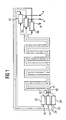
- Fig. 1 the structure of a protective circuit for an integrated circuit is shown schematically. It shows three separate, parallel tracks 10, 11, 12. These tracks 10, 11, 12 are meandering and cover a certain area in a circuit plane of the integrated circuit.
- the conductor tracks 10, 11, 12 are each connected to a separate signal generator 20, 21, 22. About the signal generators 20, 21, 22 are independent and thus in principle also different signals in the tracks 10, 11, 12 fed.
- the injected signals pass through the printed conductors 10, 11, 12 and are analyzed at the end of the printed conductors 10, 11, 12 by means of a detector 30, 31, 32 assigned to each printed conductor.
- the different signals received via the printed conductors 10, 11, 12 are compared with the reference signals fed via connecting lines 13, 14, 15 between the generators 20, 21, 22 and the detectors 30, 31, 32 associated therewith.
- the reference signals either directly represent the signals as they appear after passing through the tracks 10, 11, 12 or they provide the necessary information to determine from them the required information for the reference signals.
- the evaluation in the detectors 30, 31, 32 takes place by comparing the reference signals with the incoming signals obtained via the printed conductors 10, 11, 12. At the Detecting a difference, an alarm signal is generated as a control signal for the integrated circuit and passed via the each detector 30, 31, 32 associated alarm line 4 to the integrated circuit.
- the integrated circuit is transferred to a state which is referred to as a safety mode.
- a safety mode for example, the contents of the memory cells can no longer be read out, since, for example, they were completely deleted immediately after the transition to security mode and thus the information contained therein was irretrievably lost. Thus, it is no longer possible to read or manipulate the important information contained in program and data storage integrated circuit, such as code or PIN numbers or personal data of the user.
- the conductor tracks 10, 11, 12 are formed with such a narrow track width that any bore for overcoming the circuit levels 2, 3 of the protection circuit leads to an interruption of a conductor track. For this purpose, it is necessary to choose the distance of the individual conductor tracks 10, 11, 12 very small and to arrange the conductor closely meandered in the one or more circuit levels. Thus, an absolutely secure interruption is provided by an observation or manipulation to be prevented, in that the signal on this interrupted track 10, 11, 12 is completely interrupted and interpreted as an attack.
- the generated by the generators 20, 21, 22 signals are special, mostly digital, but also analog signals that can be a change on the transmission path via the conductor track 10, 11, 12 clearly emerge in a signal change.
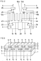
- FIG. 2 a design of another protection circuit is shown schematically.
- a single continuous strip conductor structure is given, which shows a feed point 9 for a signal formed by the one signal generator 20 in the strip conductor structure.
- the interconnect structure forms the interconnect 10a, which is the interconnect structure between the feed point 9 and the tap point of the amplifier 43 for the detector 33, the interconnect 10b between the feed point 9 and the tap point defined by the amplifier 44 for the detector 34, depending on the respective tap point. the trace 10c between the feed point 9 and the tap point for the amplifier 45 for the detector 35 and the trace 10d between the feed point 9 and the tap point for the amplifier 46 to the detector 36th
- Each of the detectors operates independently of the other detectors and can control the integrated circuit via its alarm line 4 in such a way that it is put into the safety mode.
- the generator 20 is connected via the connecting lines 16, 17, 18, 19 to the detectors 33, 34, 35, 36 and transmits these detectors the specific information for the reference signals for monitoring the conductor track 10a, 10b, 10c, 10d.
- the generator 20 randomly selects, by software control, the nature of the injected signal and signals the detectors via the corresponding connection lines 16, 17, 18, 19 to the form of the injected signal.
- the detectors 33, 34, 35 evaluate them from the generator 20 via the connecting line 16, 17, 18, 19 by comparing it with the signal supplied by the tapping points of the conductor track 10a, 10b, 10c, 10d. If there is a significant difference, that is to say a malfunction, then each detector 33, 34, 35, 36 will alarm independently of the others via its alarm line 4 and thereby convert the integrated circuit into the security mode.
- This signal must correspond in shape and type and its time course to the reference signal, which is supplied via the connecting line 16, 17, 18, 19 from the generator 20 to the detectors 33, 34, 35, 36 directly or indirectly. It is clear that the illustrated generator 20 is capable of being software controlled to dynamically change the signal fed to the feed point 9 and thereby largely preclude observation or manipulation of the protection circuit and thus of the integrated circuit 1 protected by the protection circuit.
- FIG. 3 the layered structure of the integrated circuit 1 is shown with the protective circuit arranged above.
- Fig. 3 has been dispensed with the representation of a corresponding protection circuit on the lower side of the integrated circuit.
- Such a second protection circuit on the other side of the integrated circuit 1 shows a corresponding structure as the protection circuit shown here.
- the protection circuit is arranged above the integrated circuit 1. It shows two superimposed circuit levels 2, 3, which are separated from one another and from the integrated circuit 1 to be protected by means of an insulating layer 5. By means of this insulation layer, an electrical short circuit between the conductor tracks 10, 11 and the integrated circuit 1 is excluded.
- the conductor tracks 10 are strip-shaped and separated by strip-shaped isolation regions 6 from each other.
- the conductor tracks 10 are arranged parallel to one another in the first circuit level 2.
- a second circuit level 3 is arranged, the corresponding strip-shaped, mutually parallel conductor tracks 11 shows. These interconnects 11 are separated from each other by isolation regions 6 and thus isolated from each other.
- the conductor tracks 10 are arranged such that they completely cover the integrated circuit to be protected in cooperation with the conductor tracks 11. This complete coverage is achieved when, as viewed through the first and second circuit levels 2, each point of the integrated circuit to be protected or of the integrated circuit 1 to be protected either from the tracks 10 or from the tracks 11 or both of the tracks 10 and are also covered by traces 11.
- FIG. 4 shows an embodiment of the invention is shown with eight tracks 40 ... 47. These eight tracks 40 ... 47 are divided into two groups of four tracks 40 ... 43 and 44 ... 47 respectively. Each of the two groups is assigned only one signal generator 60 or 62 and a signal detector 61 or 63.
- the signals of the signal generators 60, 62 are the conductor groups 40 ... 43 and 44 ... 47 via demultiplexer 50 and 52 and the signals transmitted via the interconnects via multiplexers 51 and 53, the signal detectors 61 and 63, respectively.
- the signal detectors 61, 63 In order to be able to supply the required reference signals to the signal detectors 61, 63, only one connecting line 48 or 49 is necessary in this embodiment of the invention per conductor group.
- the signal detectors 61, 63 also indicate here via alarm lines 4 when the signal received via the multiplexers 51, 53 does not match the expected one.
- the demultiplexer 50 and the multiplexer are jointly controlled by a true random number generator 70 for selecting one of the tracks 40 ... 43.
- the associated demultiplexer 52 and the associated multiplexer 53 are driven by two different but similarly designed pseudo-random number generators 71, 72 which, due to their similar structure, share the same random numbers at the same times deliver.
Landscapes
- Engineering & Computer Science (AREA)
- Computer Hardware Design (AREA)
- Theoretical Computer Science (AREA)
- Physics & Mathematics (AREA)
- General Physics & Mathematics (AREA)
- Computer Security & Cryptography (AREA)
- General Engineering & Computer Science (AREA)
- Microelectronics & Electronic Packaging (AREA)
- Software Systems (AREA)
- Mathematical Physics (AREA)
- Condensed Matter Physics & Semiconductors (AREA)
- Power Engineering (AREA)
- Semiconductor Integrated Circuits (AREA)
- Storage Device Security (AREA)
- Amplifiers (AREA)
- Emergency Protection Circuit Devices (AREA)
- Protection Of Static Devices (AREA)
Priority Applications (1)
| Application Number | Priority Date | Filing Date | Title |
|---|---|---|---|
| EP99957280A EP1053518B1 (de) | 1998-11-05 | 1999-11-04 | Schutzschaltung für eine integrierte schaltung |
Applications Claiming Priority (6)
| Application Number | Priority Date | Filing Date | Title |
|---|---|---|---|
| EP98120986 | 1998-11-05 | ||
| EP98120986 | 1998-11-05 | ||
| DE19917080 | 1999-04-15 | ||
| DE19917080 | 1999-04-15 | ||
| EP99957280A EP1053518B1 (de) | 1998-11-05 | 1999-11-04 | Schutzschaltung für eine integrierte schaltung |
| PCT/EP1999/008456 WO2000028399A1 (de) | 1998-11-05 | 1999-11-04 | Schutzschaltung für eine integrierte schaltung |
Publications (2)
| Publication Number | Publication Date |
|---|---|
| EP1053518A1 EP1053518A1 (de) | 2000-11-22 |
| EP1053518B1 true EP1053518B1 (de) | 2006-07-26 |
Family
ID=26052919
Family Applications (1)
| Application Number | Title | Priority Date | Filing Date |
|---|---|---|---|
| EP99957280A Expired - Lifetime EP1053518B1 (de) | 1998-11-05 | 1999-11-04 | Schutzschaltung für eine integrierte schaltung |
Country Status (10)
| Country | Link |
|---|---|
| US (1) | US6496119B1 (es) |
| EP (1) | EP1053518B1 (es) |
| JP (1) | JP2002529928A (es) |
| KR (1) | KR100710936B1 (es) |
| CN (1) | CN1214304C (es) |
| AT (1) | ATE334437T1 (es) |
| DE (1) | DE59913706D1 (es) |
| ES (1) | ES2270623T3 (es) |
| RU (1) | RU2232420C2 (es) |
| WO (1) | WO2000028399A1 (es) |
Families Citing this family (60)
| Publication number | Priority date | Publication date | Assignee | Title |
|---|---|---|---|---|
| AU2001253818A1 (en) * | 2000-02-14 | 2001-08-20 | Christina Alvarez | Security module system, apparatus and process |
| ATE350766T1 (de) | 2000-08-21 | 2007-01-15 | Infineon Technologies Ag | Vorrichtung zum schutz einer integrierten schaltung |
| DE10044837C1 (de) | 2000-09-11 | 2001-09-13 | Infineon Technologies Ag | Schaltungsanordnung und Verfahren zum Detektieren eines unerwünschten Angriffs auf eine integrierte Schaltung |
| DE10047436A1 (de) * | 2000-09-21 | 2002-08-29 | Giesecke & Devrient Gmbh | Sicherheitsmodul |
| DE10058078C1 (de) * | 2000-11-23 | 2002-04-11 | Infineon Technologies Ag | Integrierte Schaltungsanordnung mit Analysierschutz und Verfahren zur Herstellung der Anordnung |
| US20040212017A1 (en) | 2001-08-07 | 2004-10-28 | Hirotaka Mizuno | Semiconductor device and ic card |
| US7525330B2 (en) * | 2001-11-28 | 2009-04-28 | Nxp, B.V. | Semiconductor device, card, system, and methods of initializing and checking the authenticity and the identity of the semiconductor device |
| DE10218096A1 (de) * | 2002-04-23 | 2003-11-13 | Infineon Technologies Ag | Integrierte Schaltung |
| DE10247485A1 (de) * | 2002-10-11 | 2004-04-22 | Infineon Technologies Ag | Chip mit Angriffsschutz |
| KR100517554B1 (ko) * | 2002-12-05 | 2005-09-28 | 삼성전자주식회사 | 보안 기능을 갖는 반도체 집적 회로 |
| EP1968112A3 (en) | 2003-02-04 | 2008-09-17 | Matsushita Electric Industrial Co., Ltd. | Semiconductor integrated circuit device |
| JP4250038B2 (ja) * | 2003-08-20 | 2009-04-08 | シャープ株式会社 | 半導体集積回路 |
| JP4758621B2 (ja) * | 2003-08-28 | 2011-08-31 | パナソニック株式会社 | 基本セル、端部セル、配線形状、配線方法、シールド線の配線構造 |
| JP4748929B2 (ja) * | 2003-08-28 | 2011-08-17 | パナソニック株式会社 | 保護回路および半導体装置 |
| FR2863746B1 (fr) * | 2003-12-10 | 2006-08-11 | Innova Card | Circuit integre protege par bouclier actif |
| FR2865828A1 (fr) * | 2004-01-29 | 2005-08-05 | St Microelectronics Sa | Procede de securisation du mode de test d'un circuit integre par detection d'intrusion |
| FR2865827A1 (fr) * | 2004-01-29 | 2005-08-05 | St Microelectronics Sa | Securisation du mode de test d'un circuit integre |
| DE102004008178A1 (de) * | 2004-02-19 | 2005-09-01 | Giesecke & Devrient Gmbh | Verfahren zum Erzeugen von Zufallszahlen in einem tragbaren Datenträger |
| DE102004014435A1 (de) * | 2004-03-24 | 2005-11-17 | Siemens Ag | Anordnung mit einem integrierten Schaltkreis |
| GB2412996B (en) * | 2004-04-08 | 2008-11-12 | Gore & Ass | Tamper respondent covering |
| GB0410975D0 (en) | 2004-05-17 | 2004-06-16 | Nds Ltd | Chip shielding system and method |
| JP2006228910A (ja) | 2005-02-16 | 2006-08-31 | Matsushita Electric Ind Co Ltd | 半導体装置 |
| JP2006303480A (ja) * | 2005-03-25 | 2006-11-02 | Nec Electronics Corp | 半導体装置及びその保護方法 |
| US8099783B2 (en) * | 2005-05-06 | 2012-01-17 | Atmel Corporation | Security method for data protection |
| EP1947593B1 (en) * | 2005-11-07 | 2010-10-06 | Panasonic Corporation | Portable auxiliary storage device |
| US20090024890A1 (en) * | 2006-02-09 | 2009-01-22 | Nxp B.V. | Circuit arrangement, data processing device comprising such circuit arrangement as well as method for identifying an attack on such circuit arrangement |
| US7760086B2 (en) * | 2006-11-03 | 2010-07-20 | Gore Enterprise Holdings, Inc | Tamper respondent sensor and enclosure |
| KR101299602B1 (ko) * | 2007-03-27 | 2013-08-26 | 삼성전자주식회사 | 리버스 엔지니어링을 보호하는 집적회로 |
| US7923830B2 (en) * | 2007-04-13 | 2011-04-12 | Maxim Integrated Products, Inc. | Package-on-package secure module having anti-tamper mesh in the substrate of the upper package |
| US7723998B2 (en) * | 2007-06-12 | 2010-05-25 | Itt Manufacturing Enterprises, Inc. | Integrated circuit protection and detection grid |
| US7787256B2 (en) * | 2007-08-10 | 2010-08-31 | Gore Enterprise Holdings, Inc. | Tamper respondent system |
| US9747472B2 (en) * | 2007-09-13 | 2017-08-29 | Avago Technologies General Ip (Singapore) Pte. Ltd. | Mesh grid protection |
| JP2009087988A (ja) * | 2007-09-27 | 2009-04-23 | Oki Semiconductor Co Ltd | 解析防止回路を具える半導体装置及び解析防止方法 |
| US8188860B2 (en) * | 2007-10-22 | 2012-05-29 | Infineon Technologies Ag | Secure sensor/actuator systems |
| WO2009073231A1 (en) * | 2007-12-06 | 2009-06-11 | Broadcom Corporation | Embedded package security tamper mesh |
| EP2211289A1 (en) * | 2009-01-22 | 2010-07-28 | Robert Bosch GmbH | Method and control device for protecting a sensor against manipulation |
| JP2011258693A (ja) * | 2010-06-08 | 2011-12-22 | Panasonic Corp | 保護回路と半導体装置及び電子機器 |
| JP5761947B2 (ja) * | 2010-09-02 | 2015-08-12 | キヤノン株式会社 | 半導体集積回路装置 |
| CN102455394A (zh) * | 2010-10-27 | 2012-05-16 | 上海华虹集成电路有限责任公司 | 防御侵入式攻击的装置 |
| JP5062705B1 (ja) | 2011-07-07 | 2012-10-31 | Necインフロンティア株式会社 | フレキシブルプリントケーブルおよび情報処理装置 |
| US8884757B2 (en) | 2011-07-11 | 2014-11-11 | Verifone, Inc. | Anti-tampering protection assembly |
| DE102011083419A1 (de) * | 2011-09-26 | 2013-03-28 | Siemens Aktiengesellschaft | Elektronische Baugruppe, Leiterplatte und Verfahren |
| EP2780938B1 (en) * | 2011-11-18 | 2015-09-30 | Tubitak | Active shield with electrically configurable interconnections |
| JP5263999B2 (ja) | 2011-12-16 | 2013-08-14 | Necインフロンティア株式会社 | 情報処理装置 |
| US8776260B2 (en) | 2012-09-25 | 2014-07-08 | Broadcom Corporation | Mesh grid protection system |
| CN202855734U (zh) * | 2012-10-23 | 2013-04-03 | 北京同方微电子有限公司 | 用于智能卡的有源防护装置 |
| EP2766929A1 (en) | 2012-10-29 | 2014-08-20 | Qatar Foundation | A tamper detection arrangement |
| US9323957B2 (en) * | 2013-03-01 | 2016-04-26 | Marvell World Trade Ltd. | Anti-tamper system based on dual random bits generators for integrated circuits |
| RU2552181C2 (ru) * | 2013-04-05 | 2015-06-10 | Российская Федерация, От Имени Которой Выступает Министерство Промышленности И Торговли Российской Федерации | Устройство защиты от контрафакта и фальсификации интегральных схем |
| CN103530673A (zh) * | 2013-07-25 | 2014-01-22 | 上海杉德金卡信息系统科技有限公司 | 一种基于lds技术的金融pci安全设计方法 |
| CN105891651B (zh) * | 2015-01-16 | 2019-12-10 | 恩智浦美国有限公司 | 低功率开路检测系统 |
| WO2016180977A1 (en) * | 2015-05-13 | 2016-11-17 | Nagravision S.A. | Integrated circuit chip protection against physical and/or electrical alterations |
| CN104992506A (zh) * | 2015-07-06 | 2015-10-21 | 福建升腾资讯有限公司 | 一种基于lap技术的pos机安全设计方法 |
| RU2613763C1 (ru) * | 2015-11-05 | 2017-03-21 | Владимир Петрович Куклев | Многофункциональный защищенный микровычислитель |
| FR3053503B1 (fr) | 2016-06-30 | 2019-03-29 | Stmicroelectronics (Rousset) Sas | Procede de protection d'un circuit integre, et circuit integre correspondant |
| FR3054344B1 (fr) * | 2016-07-25 | 2018-09-07 | Tiempo | Circuit integre protege. |
| EP3306517A1 (en) * | 2016-10-04 | 2018-04-11 | Nagravision S.A. | An active shield for detecting an intrusion on an integrated circuit |
| KR102413790B1 (ko) * | 2020-11-27 | 2022-06-28 | 연세대학교 산학협력단 | 칩의 보안 회로 |
| KR102327811B1 (ko) * | 2021-07-23 | 2021-11-18 | 주식회사 스탠더드시험연구소 | 중성자 차등 소멸 시간 측정 장치의 멀티플렉서를 이용한 데이터 처리 장치 및 방법 |
| CN115148118A (zh) * | 2022-07-07 | 2022-10-04 | 黑芝麻智能科技有限公司 | 柔性电路板及显示装置 |
Family Cites Families (10)
| Publication number | Priority date | Publication date | Assignee | Title |
|---|---|---|---|---|
| US4593384A (en) | 1984-12-21 | 1986-06-03 | Ncr Corporation | Security device for the secure storage of sensitive data |
| GB2182176B (en) * | 1985-09-25 | 1989-09-20 | Ncr Co | Data security device for protecting stored data |
| US4882752A (en) * | 1986-06-25 | 1989-11-21 | Lindman Richard S | Computer security system |
| JP3048429B2 (ja) * | 1991-08-14 | 2000-06-05 | 株式会社東芝 | 半導体集積回路装置 |
| US5389738A (en) | 1992-05-04 | 1995-02-14 | Motorola, Inc. | Tamperproof arrangement for an integrated circuit device |
| JPH08953A (ja) * | 1994-06-15 | 1996-01-09 | Kawasaki Heavy Ind Ltd | 半乾式脱硫方法及び装置 |
| US5533123A (en) * | 1994-06-28 | 1996-07-02 | National Semiconductor Corporation | Programmable distributed personal security |
| CA2128757C (en) * | 1994-07-25 | 1998-11-03 | Jacques Caron | Control circuit for controlling voltage supply of electric devices |
| DE19618279A1 (de) * | 1996-05-07 | 1997-11-13 | Kopp Heinrich Ag | DI-Schutzschalteinrichtung |
| US5969921A (en) * | 1998-01-29 | 1999-10-19 | Eaton Corporation | Ground fault electrical switching apparatus for coordinating tripping with a downstream ground fault switch |
-
1999
- 1999-11-04 AT AT99957280T patent/ATE334437T1/de active
- 1999-11-04 JP JP2000581520A patent/JP2002529928A/ja active Pending
- 1999-11-04 US US09/582,841 patent/US6496119B1/en not_active Expired - Lifetime
- 1999-11-04 CN CNB998033499A patent/CN1214304C/zh not_active Expired - Fee Related
- 1999-11-04 ES ES99957280T patent/ES2270623T3/es not_active Expired - Lifetime
- 1999-11-04 WO PCT/EP1999/008456 patent/WO2000028399A1/de active IP Right Grant
- 1999-11-04 EP EP99957280A patent/EP1053518B1/de not_active Expired - Lifetime
- 1999-11-04 RU RU2000120620/09A patent/RU2232420C2/ru not_active IP Right Cessation
- 1999-11-04 KR KR1020007007460A patent/KR100710936B1/ko not_active IP Right Cessation
- 1999-11-04 DE DE59913706T patent/DE59913706D1/de not_active Expired - Lifetime
Also Published As
| Publication number | Publication date |
|---|---|
| KR20010040320A (ko) | 2001-05-15 |
| ATE334437T1 (de) | 2006-08-15 |
| JP2002529928A (ja) | 2002-09-10 |
| ES2270623T3 (es) | 2007-04-01 |
| WO2000028399A1 (de) | 2000-05-18 |
| RU2232420C2 (ru) | 2004-07-10 |
| DE59913706D1 (de) | 2006-09-07 |
| EP1053518A1 (de) | 2000-11-22 |
| KR100710936B1 (ko) | 2007-04-24 |
| CN1292110A (zh) | 2001-04-18 |
| CN1214304C (zh) | 2005-08-10 |
| US6496119B1 (en) | 2002-12-17 |
Similar Documents
| Publication | Publication Date | Title |
|---|---|---|
| EP1053518B1 (de) | Schutzschaltung für eine integrierte schaltung | |
| EP1182702B1 (de) | Vorrichtung zum Schutz einer integrierten Schaltung | |
| EP1149358B1 (de) | Kontaktlose chipkarte | |
| DE102012212471B3 (de) | Vorrichtung zum Realisieren einer physikalischen Degradations-/Tampererkennung eines digitalen ICs mittels einer (digitalen) PUF und Unterscheiden zwischen einer Degradation aufgrund von physikalischer Manipulation und aufgrund von Alterungsprozessen | |
| DE3818960C2 (es) | ||
| DE102007057477B4 (de) | Vorrichtung zum Überwachen eines Raumes durch seriell verschaltete Schließkontakte, insbesondere Deckelschalter in einem Sicherungsgehäuse | |
| EP1334416B1 (de) | Schaltungsanordnung und verfahren zum detektieren eines unerwünschten angriffs auf eine integrierte schaltung | |
| DE102012109665A1 (de) | Manipulationserkennungsmaßnahmen zum Abschecken physischer Angriffe auf ein Sicherheits-ASIC | |
| DE10223176B3 (de) | Integrierte Schaltung mit sicherheitskritischen Schaltungskomponenten | |
| DE102006001873A1 (de) | Vorrichtung und Verfahren zum Überprüfen einer Fehlererkennungsfunktionaltität einer Speicherschaltung | |
| DE102004062825A1 (de) | Kryptographische Einheit und Verfahren zum Betreiben einer kryptographischen Einheit | |
| EP0992809A1 (de) | Schaltungsanordnung mit deaktivierbarem Scanpfad | |
| EP2666117B1 (de) | Verfahren zum prüfen eines tamperschutzes eines feldgeräts sowie feldgerät mit tamperschutz | |
| EP1222621B1 (de) | Integrierter schaltkreis und schaltungsanordnung zur stromversorgung eines integrierten schaltkreises | |
| DE10326089B3 (de) | Manipulationsüberwachung für eine Schaltung | |
| DE10347301B4 (de) | Schaltung mit einem Bus mit mehreren Empfängern | |
| DE10045025A1 (de) | IC-Packung mit einer Sicherheitseinrichtung | |
| EP3839683A1 (de) | System mit selbstprüffunktion und verfahren zum verifizieren der selbstprüffunktion eines systems | |
| EP3401831B1 (de) | Vorrichtung und verfahren zum erkennen einer physikalischen manipulation an einem elektronischen sicherheitsmodul | |
| DE10258178B4 (de) | Schaltung mit Sicherheitsmaßnahmen gegen Ausspionieren der Schaltung | |
| EP1058178B1 (de) | Schutzschaltung | |
| AT507122B1 (de) | Verfahren zum betrieb einer transaktionsbasierten ablaufsteuerung | |
| EP0771094B1 (de) | Verfahren und Anordnung zur Herstellung und Erkennung der Authentizität von Befehlssignalen | |
| WO2021144145A1 (de) | Schaltungsanordnung eines elektronischen siegels | |
| EP2099265A2 (de) | Leiterbahnanordnung zum Kontaktieren elektronischer Bauteile |
Legal Events
| Date | Code | Title | Description |
|---|---|---|---|
| PUAI | Public reference made under article 153(3) epc to a published international application that has entered the european phase |
Free format text: ORIGINAL CODE: 0009012 |
|
| 17P | Request for examination filed |
Effective date: 20000807 |
|
| AK | Designated contracting states |
Kind code of ref document: A1 Designated state(s): AT BE CH CY DE DK ES FI FR GB GR IE IT LI LU MC NL PT SE |
|
| 17Q | First examination report despatched |
Effective date: 20020318 |
|
| GRAP | Despatch of communication of intention to grant a patent |
Free format text: ORIGINAL CODE: EPIDOSNIGR1 |
|
| GRAS | Grant fee paid |
Free format text: ORIGINAL CODE: EPIDOSNIGR3 |
|
| GRAA | (expected) grant |
Free format text: ORIGINAL CODE: 0009210 |
|
| AK | Designated contracting states |
Kind code of ref document: B1 Designated state(s): AT BE CH CY DE DK ES FI FR GB GR IE IT LI LU MC NL PT SE |
|
| PG25 | Lapsed in a contracting state [announced via postgrant information from national office to epo] |
Ref country code: NL Free format text: LAPSE BECAUSE OF FAILURE TO SUBMIT A TRANSLATION OF THE DESCRIPTION OR TO PAY THE FEE WITHIN THE PRESCRIBED TIME-LIMIT Effective date: 20060726 Ref country code: IT Free format text: LAPSE BECAUSE OF FAILURE TO SUBMIT A TRANSLATION OF THE DESCRIPTION OR TO PAY THE FEE WITHIN THE PRE;WARNING: LAPSES OF ITALIAN PATENTS WITH EFFECTIVE DATE BEFORE 2007 MAY HAVE OCCURRED AT ANY TIME BEFORE 2007. THE CORRECT EFFECTIVE DATE MAY BE DIFFERENT FROM THE ONE RECORDED.SCRIBED TIME-LIMIT Effective date: 20060726 Ref country code: IE Free format text: LAPSE BECAUSE OF FAILURE TO SUBMIT A TRANSLATION OF THE DESCRIPTION OR TO PAY THE FEE WITHIN THE PRESCRIBED TIME-LIMIT Effective date: 20060726 Ref country code: FI Free format text: LAPSE BECAUSE OF FAILURE TO SUBMIT A TRANSLATION OF THE DESCRIPTION OR TO PAY THE FEE WITHIN THE PRESCRIBED TIME-LIMIT Effective date: 20060726 |
|
| RBV | Designated contracting states (corrected) |
Designated state(s): AT BE CH CY DE DK ES FI FR GB GR IE IT LI LU MC NL PT SE |
|
| REG | Reference to a national code |
Ref country code: GB Ref legal event code: FG4D Free format text: NOT ENGLISH |
|
| REG | Reference to a national code |
Ref country code: CH Ref legal event code: EP |
|
| REG | Reference to a national code |
Ref country code: IE Ref legal event code: FG4D Free format text: LANGUAGE OF EP DOCUMENT: GERMAN |
|
| REF | Corresponds to: |
Ref document number: 59913706 Country of ref document: DE Date of ref document: 20060907 Kind code of ref document: P |
|
| PG25 | Lapsed in a contracting state [announced via postgrant information from national office to epo] |
Ref country code: SE Free format text: LAPSE BECAUSE OF FAILURE TO SUBMIT A TRANSLATION OF THE DESCRIPTION OR TO PAY THE FEE WITHIN THE PRESCRIBED TIME-LIMIT Effective date: 20061026 Ref country code: DK Free format text: LAPSE BECAUSE OF FAILURE TO SUBMIT A TRANSLATION OF THE DESCRIPTION OR TO PAY THE FEE WITHIN THE PRESCRIBED TIME-LIMIT Effective date: 20061026 |
|
| GBT | Gb: translation of ep patent filed (gb section 77(6)(a)/1977) |
Effective date: 20061018 |
|
| REG | Reference to a national code |
Ref country code: CH Ref legal event code: NV Representative=s name: INFINEON TECHNOLOGIES SCHWEIZ AG |
|
| PG25 | Lapsed in a contracting state [announced via postgrant information from national office to epo] |
Ref country code: MC Free format text: LAPSE BECAUSE OF NON-PAYMENT OF DUE FEES Effective date: 20061130 Ref country code: BE Free format text: LAPSE BECAUSE OF NON-PAYMENT OF DUE FEES Effective date: 20061130 |
|
| PG25 | Lapsed in a contracting state [announced via postgrant information from national office to epo] |
Ref country code: PT Free format text: LAPSE BECAUSE OF FAILURE TO SUBMIT A TRANSLATION OF THE DESCRIPTION OR TO PAY THE FEE WITHIN THE PRESCRIBED TIME-LIMIT Effective date: 20061226 |
|
| NLV1 | Nl: lapsed or annulled due to failure to fulfill the requirements of art. 29p and 29m of the patents act | ||
| ET | Fr: translation filed | ||
| REG | Reference to a national code |
Ref country code: ES Ref legal event code: FG2A Ref document number: 2270623 Country of ref document: ES Kind code of ref document: T3 |
|
| PLBE | No opposition filed within time limit |
Free format text: ORIGINAL CODE: 0009261 |
|
| STAA | Information on the status of an ep patent application or granted ep patent |
Free format text: STATUS: NO OPPOSITION FILED WITHIN TIME LIMIT |
|
| 26N | No opposition filed |
Effective date: 20070427 |
|
| BERE | Be: lapsed |
Owner name: SIEMENS A.G. Effective date: 20061130 Owner name: INFINEON TECHNOLOGIES A.G. Effective date: 20061130 |
|
| PG25 | Lapsed in a contracting state [announced via postgrant information from national office to epo] |
Ref country code: GR Free format text: LAPSE BECAUSE OF FAILURE TO SUBMIT A TRANSLATION OF THE DESCRIPTION OR TO PAY THE FEE WITHIN THE PRESCRIBED TIME-LIMIT Effective date: 20061027 |
|
| PG25 | Lapsed in a contracting state [announced via postgrant information from national office to epo] |
Ref country code: LU Free format text: LAPSE BECAUSE OF NON-PAYMENT OF DUE FEES Effective date: 20061104 |
|
| PG25 | Lapsed in a contracting state [announced via postgrant information from national office to epo] |
Ref country code: CY Free format text: LAPSE BECAUSE OF FAILURE TO SUBMIT A TRANSLATION OF THE DESCRIPTION OR TO PAY THE FEE WITHIN THE PRESCRIBED TIME-LIMIT Effective date: 20060726 |
|
| REG | Reference to a national code |
Ref country code: CH Ref legal event code: PFA Owner name: SIEMENS AKTIENGESELLSCHAFT Free format text: SIEMENS AKTIENGESELLSCHAFT#WITTELSBACHERPLATZ 2#80333 MUENCHEN (DE) $ INFINEON TECHNOLOGIES AG#ST.-MARTIN-STRASSE 53#81669 MUENCHEN (DE) -TRANSFER TO- SIEMENS AKTIENGESELLSCHAFT#WITTELSBACHERPLATZ 2#80333 MUENCHEN (DE) $ INFINEON TECHNOLOGIES AG#ST.-MARTIN-STRASSE 53#81669 MUENCHEN (DE) |
|
| REG | Reference to a national code |
Ref country code: DE Ref legal event code: R081 Ref document number: 59913706 Country of ref document: DE Owner name: INFINEON TECHNOLOGIES AG, DE Free format text: FORMER OWNERS: SIEMENS AKTIENGESELLSCHAFT, 80333 MUENCHEN, DE; INFINEON TECHNOLOGIES AG, 81669 MUENCHEN, DE Effective date: 20140708 Ref country code: DE Ref legal event code: R081 Ref document number: 59913706 Country of ref document: DE Owner name: INFINEON TECHNOLOGIES AG, DE Free format text: FORMER OWNER: SIEMENS AKTIENGESELLSCHAFT, INFINEON TECHNOLOGIES AG, , DE Effective date: 20140708 |
|
| REG | Reference to a national code |
Ref country code: FR Ref legal event code: PLFP Year of fee payment: 17 |
|
| REG | Reference to a national code |
Ref country code: FR Ref legal event code: PLFP Year of fee payment: 18 |
|
| REG | Reference to a national code |
Ref country code: CH Ref legal event code: NV Representative=s name: E. BLUM AND CO. AG PATENT- UND MARKENANWAELTE , CH |
|
| REG | Reference to a national code |
Ref country code: CH Ref legal event code: PCOW Free format text: NEW ADDRESS: ST.-MARTIN-STRASSE 53, 81669 MUENCHEN (DE) $ SIEMENS AKTIENGESELLSCHAFT, WERNER-VON-SIEMENS-STRASSE 1, 80333 MUENCHEN (DE) |
|
| REG | Reference to a national code |
Ref country code: FR Ref legal event code: PLFP Year of fee payment: 19 |
|
| PGFP | Annual fee paid to national office [announced via postgrant information from national office to epo] |
Ref country code: FR Payment date: 20171121 Year of fee payment: 19 |
|
| PGFP | Annual fee paid to national office [announced via postgrant information from national office to epo] |
Ref country code: AT Payment date: 20171121 Year of fee payment: 19 Ref country code: IT Payment date: 20171124 Year of fee payment: 19 Ref country code: CH Payment date: 20171120 Year of fee payment: 19 Ref country code: GB Payment date: 20171123 Year of fee payment: 19 Ref country code: ES Payment date: 20171220 Year of fee payment: 19 |
|
| PGFP | Annual fee paid to national office [announced via postgrant information from national office to epo] |
Ref country code: DE Payment date: 20180118 Year of fee payment: 19 |
|
| REG | Reference to a national code |
Ref country code: DE Ref legal event code: R119 Ref document number: 59913706 Country of ref document: DE |
|
| REG | Reference to a national code |
Ref country code: CH Ref legal event code: PL |
|
| REG | Reference to a national code |
Ref country code: AT Ref legal event code: MM01 Ref document number: 334437 Country of ref document: AT Kind code of ref document: T Effective date: 20181104 |
|
| GBPC | Gb: european patent ceased through non-payment of renewal fee |
Effective date: 20181104 |
|
| PG25 | Lapsed in a contracting state [announced via postgrant information from national office to epo] |
Ref country code: LI Free format text: LAPSE BECAUSE OF NON-PAYMENT OF DUE FEES Effective date: 20181130 Ref country code: CH Free format text: LAPSE BECAUSE OF NON-PAYMENT OF DUE FEES Effective date: 20181130 |
|
| PG25 | Lapsed in a contracting state [announced via postgrant information from national office to epo] |
Ref country code: IT Free format text: LAPSE BECAUSE OF NON-PAYMENT OF DUE FEES Effective date: 20181104 Ref country code: DE Free format text: LAPSE BECAUSE OF NON-PAYMENT OF DUE FEES Effective date: 20190601 Ref country code: AT Free format text: LAPSE BECAUSE OF NON-PAYMENT OF DUE FEES Effective date: 20181104 Ref country code: FR Free format text: LAPSE BECAUSE OF NON-PAYMENT OF DUE FEES Effective date: 20181130 |
|
| PG25 | Lapsed in a contracting state [announced via postgrant information from national office to epo] |
Ref country code: GB Free format text: LAPSE BECAUSE OF NON-PAYMENT OF DUE FEES Effective date: 20181104 |
|
| REG | Reference to a national code |
Ref country code: ES Ref legal event code: FD2A Effective date: 20200102 |
|
| PG25 | Lapsed in a contracting state [announced via postgrant information from national office to epo] |
Ref country code: ES Free format text: LAPSE BECAUSE OF NON-PAYMENT OF DUE FEES Effective date: 20181105 |