EP1045461A2 - Verfahren zur Herstellung von Hallelementen - Google Patents
Verfahren zur Herstellung von Hallelementen Download PDFInfo
- Publication number
- EP1045461A2 EP1045461A2 EP00810082A EP00810082A EP1045461A2 EP 1045461 A2 EP1045461 A2 EP 1045461A2 EP 00810082 A EP00810082 A EP 00810082A EP 00810082 A EP00810082 A EP 00810082A EP 1045461 A2 EP1045461 A2 EP 1045461A2
- Authority
- EP
- European Patent Office
- Prior art keywords
- conductivity type
- implantation
- subsequent
- hall element
- area
- Prior art date
- Legal status (The legal status is an assumption and is not a legal conclusion. Google has not performed a legal analysis and makes no representation as to the accuracy of the status listed.)
- Withdrawn
Links
- 238000004519 manufacturing process Methods 0.000 title claims abstract description 11
- 230000005355 Hall effect Effects 0.000 title 1
- 238000009792 diffusion process Methods 0.000 claims abstract description 29
- 238000002513 implantation Methods 0.000 claims abstract description 23
- 238000000034 method Methods 0.000 claims abstract description 8
- 230000001427 coherent effect Effects 0.000 claims description 2
- 239000004065 semiconductor Substances 0.000 abstract description 7
- 230000035945 sensitivity Effects 0.000 description 8
- 239000002800 charge carrier Substances 0.000 description 6
- 239000000243 solution Substances 0.000 description 6
- 238000005516 engineering process Methods 0.000 description 5
- 101100269850 Caenorhabditis elegans mask-1 gene Proteins 0.000 description 4
- 239000000758 substrate Substances 0.000 description 4
- XUIMIQQOPSSXEZ-UHFFFAOYSA-N Silicon Chemical compound [Si] XUIMIQQOPSSXEZ-UHFFFAOYSA-N 0.000 description 3
- 150000002500 ions Chemical class 0.000 description 3
- 229910052710 silicon Inorganic materials 0.000 description 3
- 239000010703 silicon Substances 0.000 description 3
- 230000001419 dependent effect Effects 0.000 description 2
- TZCXTZWJZNENPQ-UHFFFAOYSA-L barium sulfate Chemical compound [Ba+2].[O-]S([O-])(=O)=O TZCXTZWJZNENPQ-UHFFFAOYSA-L 0.000 description 1
- 230000000694 effects Effects 0.000 description 1
- 230000010354 integration Effects 0.000 description 1
- 238000005259 measurement Methods 0.000 description 1
- 238000010079 rubber tapping Methods 0.000 description 1
Images
Classifications
-
- G—PHYSICS
- G01—MEASURING; TESTING
- G01R—MEASURING ELECTRIC VARIABLES; MEASURING MAGNETIC VARIABLES
- G01R33/00—Arrangements or instruments for measuring magnetic variables
- G01R33/02—Measuring direction or magnitude of magnetic fields or magnetic flux
- G01R33/06—Measuring direction or magnitude of magnetic fields or magnetic flux using galvano-magnetic devices
- G01R33/07—Hall effect devices
Definitions
- the invention relates to a method for producing Hall elements in the preamble of Claim 1 mentioned type.
- the invention is based on the object of specifying a method for producing Hall elements, where the Hall element is on the same chip as the electronics, without additional Process steps are required.
- the Implantation for the area of the second conductivity type uses a mask in which a larger one Part of the area of the area of the second conductivity type that this area follows Diffusion or the subsequent diffusions is covered. So it is e.g. particularly advantageous during implantation, at least two areas of the second conductivity type which are separate from one another to form, whose distance is dimensioned so that the at least two areas in the diffusion to unite the contiguous area.
- the effective density of the implanted ions and thus the movable charge carriers - electrons or holes - can be calculated according to the ratio of Reduce the covered area to the total area of the area of the second conductivity type.
- Hall elements without the disadvantages mentioned above on one Integrate electronics chip.
- Another way to increase the sensitivity of a Hall element, without having to put up with a process change consists of the implantation in the area that will later serve as a magnetic field sensitive zone, a mask with two crossed arranged to use slots that are very narrow compared to the depth of the area after the Are diffusion. In the case of diffusion, the area of the second conductivity type widens as a result of the lateral diffusion very strong.
- the effective charge carrier density, the sensitivity of the Hall element decisively determined, is thus significantly reduced during diffusion.
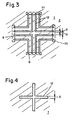
- the Hall element 3 is used to measure a magnetic field B flowing through its surface 4 in the vertical direction and is produced, for example, in a CMOS or bipolar technology.
- a silicon substrate 7 of a first conductivity type serves as the substrate.
- the Hall element 3 comprises an area 5 serving for the measurement of the magnetic field B, which is realized as a trough 6 of a second conductivity type in the silicon substrate 7, and four electrodes 8-11. Via the four electrodes 8-11, they are designed as highly doped areas of the second conductivity type are, the tub 6 is electrically contacted.
- the two electrodes 8 and 10 lying opposite one another serve as current contacts for feeding in a current I.
- the electrodes 9 and 11 serve as voltage electrodes for tapping off the Hall voltage U H which arises between them in the presence of the magnetic field B.
- the trough 6 is preferably an n-doped trough, since the mobility of the electrons is greater than the mobility of the holes.
- the n-well 6 is produced by an implantation and subsequent diffusion process.
- the size N S is therefore equal to the number of ions implanted per unit area, the implanted dose Q.
- the invention now consists in covering a comparatively large proportion of the surface of the n-well 6 to be formed for the Hall element 3 for the implantation.
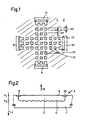
- the mask 1 (FIG. 1) used to create the n-well therefore does not have a single large window in the Hall element 3, the outline of which corresponds to the shape of the Hall element 3 (cross shape in FIG. 1), but a large number of small windows 12 on.
- the distances d 1 between the windows 12 are smaller than the depth x 2 that the n-well 6 reaches during the diffusion process following the implantation (and possibly further diffusion processes). Since the distance d 1 between the windows 12 is smaller than the distance x 2 , a coherent n-well is formed in the diffusion process due to the laterally occurring diffusion.
- the small windows 12 are arranged next to one another in a matrix-like manner such that the continuous n-well 6 is formed during the diffusion as a magnetic field-sensitive area.
- the depth x 2 of the n-well 6 is, for example, approximately 1 to 2 ⁇ m.
- the dose implanted in the silicon substrate 7 can be reduced by a factor of 4, since three quarters of the magnetic field-sensitive during implantation compared to conventional manufacturing methods Area 5 of the Hall element 3 are covered.
- the effective dose Q eff is therefore a factor 4 smaller than the dose Q delivered by the implanter. Consequently, the density of the free charge carriers N S in the tub 6 is also 4 times smaller and the current-related sensitivity S I of the Hall element produced in this way 3 larger by a factor of 4.
- the distance d 1 could also be chosen somewhat larger than the distance x 2 , since the lateral diffusion always starts from two neighboring windows 12, the diffusion fronts meeting in the middle between the windows 12 and thus the electrical connection to a single n - effect tub 6.
- Fig. 1 the layout of the mask 2 is shown with dashed lines, which during the implantation of the Electrodes 8-11 are used.
- the windows 12 of the mask 1, which are adjacent to the windows 13, are connected to each other to form a larger window 12 ', so that during manufacture within possible misalignment between the masks 1 and 2 of certain tolerance limits causes small offset errors.
- the invention can be used not only for increasing the sensitivity of an electronic chip use integrated Hall element.
- the invention can also be used to point to the same To produce chip n wells of different conductivity, which e.g. as resistors with different Resistance value can be used.
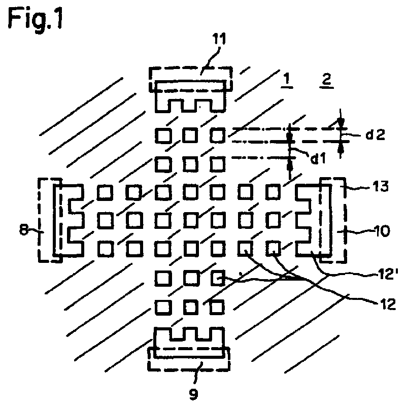
- the windows 12 are in the form of slots.
- the width S of the slots is smaller than the depth x 2 that the n-well 6 reaches in the subsequent diffusions.
- the windows in the implantation mask 2 which are provided for the doping of the electrodes 8-11 are shown with dashed lines.
- the distance D of the slots is approximately one to two times the depth x 2 . However, the distance D is chosen to be at most large enough that a single continuous n-well 6 is formed in the subsequent diffusions. The advantage here is that the effective dose Q eff is significantly smaller than the dose Q delivered by the implanter.
- FIG. 4 shows the layout of the mask 1 to be used in the implantation for a cross-shaped Hall element 3, which is formed by only two slots (window 12), the width S of which is substantially smaller than the depth x 2 .
Landscapes
- Physics & Mathematics (AREA)
- Condensed Matter Physics & Semiconductors (AREA)
- General Physics & Mathematics (AREA)
- Hall/Mr Elements (AREA)
Abstract
Description
- Fig. 1
- Implantationsmasken für ein Hallelement,
- Fig. 2
- das Hallelement im Querschnitt, und
- Fig. 3, 4
- weitere Implantationsmasken für weitere Hallelemente.
- Die strombezogene Empfindlichkeit des Hallelementes SI erhöht sich gegenüber einem
konventionellen Hallelement, dessen n-Wanne um ein Vielfaches breiter als seine Tiefe x2 ist, um etwa
den Faktor

- Das magnetfeldempfindliche Volumen des Hallelementes wird äusserst klein, so dass das Magnetfeld mit hoher örtlicher Auflösung gemessen werden kann.
Claims (4)
- Verfahren zur Herstellung eines Hallelementes (3), bei dem durch Implantation und eine oder mehrere nachfolgende Diffusionen innerhalb eines Gebietes eines ersten Leitfähigkeittyps (7) ein zusammenhängendes Gebiet (6) eines zweiten Leitfähigkeittyps gebildet wird, dadurch gekennzeichnet, dass bei der Implantation mindestens zwei voneinander getrennte Gebiete des zweiten Leitfähigkeittyps gebildet werden, deren Abstand so bemessen ist, dass sich die mindestens zwei Gebiete bei der nachfolgenden oder den nachfolgenden Diffusionen zu dem zusammenhängenden Gebiet (6) vereinigen.
- Verfahren nach Anspruch 1, dadurch gekennzeichnet, dass bei der Implantation zur Bildung des zusammenhängenden Gebietes (6) des zweiten Leitfähigkeittyps eine Maske (1) mit Fenstern (12) verwendet wird, deren Abmessungen kleiner als die Tiefe (x2) des zusammenhängenden Gebietes (6) nach der nachfolgenden oder den nachfolgenden Diffusionen ist.
- Verfahren nach Anspruch 1, dadurch gekennzeichnet, dass bei der Implantation zur Bildung des zusammenhängenden Gebietes (6) des zweiten Leitfähigkeittyps eine Maske (1) mit Fenstern (12) verwendet wird, die als Schlitze ausgebildet sind, deren Breite (S) kleiner als die Tiefe (x2) des zusammenhängenden Gebietes (6) nach der nachfolgenden oder den nachfolgenden Diffusionen ist.
- Verfahren zur Herstellung eines Hallelementes (3), bei dem durch Implantation und nachfolgende Diffusion innerhalb eines Gebietes eines ersten Leitfähigkeittyps (7) ein zusammenhängendes Gebiet (6) eines zweiten Leitfähigkeittyps gebildet wird, dadurch gekennzeichnet, dass bei der Implantation eine Maske mit zwei kreuzförmig angeordneten Schlitzen verwendet wird, wobei die Breite (S) der Schlitze kleiner als die Tiefe (x2) ist die das Gebiet (6) des zweiten Leitfähigkeittyps nach der nachfolgenden oder den nachfolgenden Diffusionen aufweist.
Applications Claiming Priority (4)
| Application Number | Priority Date | Filing Date | Title |
|---|---|---|---|
| CH17499 | 1999-02-01 | ||
| CH174992000 | 1999-02-01 | ||
| CH194099 | 1999-10-21 | ||
| CH194099 | 1999-10-21 |
Publications (2)
| Publication Number | Publication Date |
|---|---|
| EP1045461A2 true EP1045461A2 (de) | 2000-10-18 |
| EP1045461A3 EP1045461A3 (de) | 2005-02-09 |
Family
ID=25683758
Family Applications (1)
| Application Number | Title | Priority Date | Filing Date |
|---|---|---|---|
| EP00810082A Withdrawn EP1045461A3 (de) | 1999-02-01 | 2000-01-28 | Verfahren zur Herstellung von Hallelementen |
Country Status (1)
| Country | Link |
|---|---|
| EP (1) | EP1045461A3 (de) |
Family Cites Families (2)
| Publication number | Priority date | Publication date | Assignee | Title |
|---|---|---|---|---|
| SI9110476A (en) * | 1991-03-18 | 1996-02-29 | Iskra Stevci Ind Merilne In Up | Hall sensor in integrated CMOS circuit |
| US5300454A (en) * | 1992-11-24 | 1994-04-05 | Motorola, Inc. | Method for forming doped regions within a semiconductor substrate |
-
2000
- 2000-01-28 EP EP00810082A patent/EP1045461A3/de not_active Withdrawn
Also Published As
| Publication number | Publication date |
|---|---|
| EP1045461A3 (de) | 2005-02-09 |
Similar Documents
| Publication | Publication Date | Title |
|---|---|---|
| DE3889245T2 (de) | Integrierter und kontrollierter Leistungs-MOSFET. | |
| DE69128566T2 (de) | Zusammengesetzte integrierte Schaltungsanordnung | |
| DE2214935C2 (de) | Integrierte MOS-Schaltung | |
| DE69835183T2 (de) | Verwendung eines getarnten Schaltkreises | |
| DE4112072C2 (de) | MIS-Transistor mit hoher Stehspannung und Verfahren zu seiner Herstellung | |
| DE102014212651B4 (de) | Widerstandselement mit spezifischem Piezowiderstandskoeffizienten, stresskompensiertes Sensorsystem und Verfahren | |
| DE1614373C2 (de) | ||
| DE19501557C2 (de) | CMOS-Halbleitervorrichtung und Verfahren zu deren Herstellung | |
| DE69327556T2 (de) | Verfahren zur Herstellung eines dynamischen Halbleitersensors mit einer Struktur mit dünner Stärke | |
| DE2655400A1 (de) | Halbleitervorrichtung und verfahren zu ihrer herstellung | |
| DE2242026A1 (de) | Mis-feldeffekttransistor | |
| EP2503612A2 (de) | Vertikaler Hallsensor und Verfahren zur Herstellung eines vertikalen Hallsensors | |
| DE69518571T2 (de) | Schutzanordnung gegen elektrostatische Entladungen | |
| DE2342637A1 (de) | Zenerdiode mit drei elektrischen anschlussbereichen | |
| DE3714790A1 (de) | Zenerdiode unter der oberflaeche und herstellungsverfahren | |
| DE19733974A1 (de) | MOSFET-Einrichtung | |
| DE10224003B4 (de) | Halbleitervorrichtung und Verfahren für ihre Herstellung | |
| DE1808928A1 (de) | Halbleiterbauelement und Verfahren zu dessen Herstellung | |
| DE69117988T2 (de) | Halbleitervorrichtung mit Ladungstransfer-Bauelement, MOSFETs und Bipolartransistoren - alle in einem einzelnen Halbleitersubstrat gebildet | |
| DE19710233A1 (de) | Halbleitereinrichtung und Herstellungsverfahren derselben | |
| DE2953394C2 (de) | ||
| DE10109174A1 (de) | Verfahren zum Strukturentwurf von integrierten Halbleiterschaltungen und Vorrichtung zur Durchführung desselben | |
| DE3119288A1 (de) | Halbleiteranordnung | |
| DE3842749A1 (de) | Verfahren zum herstellen einer integrierten schaltung | |
| DE10247431A1 (de) | Halbleitervorrichtung |
Legal Events
| Date | Code | Title | Description |
|---|---|---|---|
| PUAI | Public reference made under article 153(3) epc to a published international application that has entered the european phase |
Free format text: ORIGINAL CODE: 0009012 |
|
| AK | Designated contracting states |
Kind code of ref document: A2 Designated state(s): AT BE CH CY DE DK ES FI FR GB GR IE IT LI LU MC NL PT SE |
|
| AX | Request for extension of the european patent |
Free format text: AL;LT;LV;MK;RO;SI |
|
| PUAL | Search report despatched |
Free format text: ORIGINAL CODE: 0009013 |
|
| AK | Designated contracting states |
Kind code of ref document: A3 Designated state(s): AT BE CH CY DE DK ES FI FR GB GR IE IT LI LU MC NL PT SE |
|
| AX | Request for extension of the european patent |
Extension state: AL LT LV MK RO SI |
|
| STAA | Information on the status of an ep patent application or granted ep patent |
Free format text: STATUS: THE APPLICATION HAS BEEN WITHDRAWN |
|
| 18W | Application withdrawn |
Effective date: 20050218 |