EP1045461A2 - Method of making Hall-effect devices - Google Patents
Method of making Hall-effect devices Download PDFInfo
- Publication number
- EP1045461A2 EP1045461A2 EP00810082A EP00810082A EP1045461A2 EP 1045461 A2 EP1045461 A2 EP 1045461A2 EP 00810082 A EP00810082 A EP 00810082A EP 00810082 A EP00810082 A EP 00810082A EP 1045461 A2 EP1045461 A2 EP 1045461A2
- Authority
- EP
- European Patent Office
- Prior art keywords
- conductivity type
- implantation
- subsequent
- hall element
- area
- Prior art date
- Legal status (The legal status is an assumption and is not a legal conclusion. Google has not performed a legal analysis and makes no representation as to the accuracy of the status listed.)
- Withdrawn
Links
- 238000004519 manufacturing process Methods 0.000 title claims abstract description 11
- 230000005355 Hall effect Effects 0.000 title 1
- 238000009792 diffusion process Methods 0.000 claims abstract description 29
- 238000002513 implantation Methods 0.000 claims abstract description 23
- 238000000034 method Methods 0.000 claims abstract description 8
- 230000001427 coherent effect Effects 0.000 claims description 2
- 239000004065 semiconductor Substances 0.000 abstract description 7
- 230000035945 sensitivity Effects 0.000 description 8
- 239000002800 charge carrier Substances 0.000 description 6
- 239000000243 solution Substances 0.000 description 6
- 238000005516 engineering process Methods 0.000 description 5
- 101100269850 Caenorhabditis elegans mask-1 gene Proteins 0.000 description 4
- 239000000758 substrate Substances 0.000 description 4
- XUIMIQQOPSSXEZ-UHFFFAOYSA-N Silicon Chemical compound [Si] XUIMIQQOPSSXEZ-UHFFFAOYSA-N 0.000 description 3
- 150000002500 ions Chemical class 0.000 description 3
- 229910052710 silicon Inorganic materials 0.000 description 3
- 239000010703 silicon Substances 0.000 description 3
- 230000001419 dependent effect Effects 0.000 description 2
- TZCXTZWJZNENPQ-UHFFFAOYSA-L barium sulfate Chemical compound [Ba+2].[O-]S([O-])(=O)=O TZCXTZWJZNENPQ-UHFFFAOYSA-L 0.000 description 1
- 230000000694 effects Effects 0.000 description 1
- 230000010354 integration Effects 0.000 description 1
- 238000005259 measurement Methods 0.000 description 1
- 238000010079 rubber tapping Methods 0.000 description 1
Images
Classifications
-
- G—PHYSICS
- G01—MEASURING; TESTING
- G01R—MEASURING ELECTRIC VARIABLES; MEASURING MAGNETIC VARIABLES
- G01R33/00—Arrangements or instruments for measuring magnetic variables
- G01R33/02—Measuring direction or magnitude of magnetic fields or magnetic flux
- G01R33/06—Measuring direction or magnitude of magnetic fields or magnetic flux using galvano-magnetic devices
- G01R33/07—Hall effect devices
Definitions
- the invention relates to a method for producing Hall elements in the preamble of Claim 1 mentioned type.
- the invention is based on the object of specifying a method for producing Hall elements, where the Hall element is on the same chip as the electronics, without additional Process steps are required.
- the Implantation for the area of the second conductivity type uses a mask in which a larger one Part of the area of the area of the second conductivity type that this area follows Diffusion or the subsequent diffusions is covered. So it is e.g. particularly advantageous during implantation, at least two areas of the second conductivity type which are separate from one another to form, whose distance is dimensioned so that the at least two areas in the diffusion to unite the contiguous area.
- the effective density of the implanted ions and thus the movable charge carriers - electrons or holes - can be calculated according to the ratio of Reduce the covered area to the total area of the area of the second conductivity type.
- Hall elements without the disadvantages mentioned above on one Integrate electronics chip.
- Another way to increase the sensitivity of a Hall element, without having to put up with a process change consists of the implantation in the area that will later serve as a magnetic field sensitive zone, a mask with two crossed arranged to use slots that are very narrow compared to the depth of the area after the Are diffusion. In the case of diffusion, the area of the second conductivity type widens as a result of the lateral diffusion very strong.
- the effective charge carrier density, the sensitivity of the Hall element decisively determined, is thus significantly reduced during diffusion.
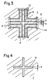
- the Hall element 3 is used to measure a magnetic field B flowing through its surface 4 in the vertical direction and is produced, for example, in a CMOS or bipolar technology.
- a silicon substrate 7 of a first conductivity type serves as the substrate.
- the Hall element 3 comprises an area 5 serving for the measurement of the magnetic field B, which is realized as a trough 6 of a second conductivity type in the silicon substrate 7, and four electrodes 8-11. Via the four electrodes 8-11, they are designed as highly doped areas of the second conductivity type are, the tub 6 is electrically contacted.
- the two electrodes 8 and 10 lying opposite one another serve as current contacts for feeding in a current I.
- the electrodes 9 and 11 serve as voltage electrodes for tapping off the Hall voltage U H which arises between them in the presence of the magnetic field B.
- the trough 6 is preferably an n-doped trough, since the mobility of the electrons is greater than the mobility of the holes.
- the n-well 6 is produced by an implantation and subsequent diffusion process.
- the size N S is therefore equal to the number of ions implanted per unit area, the implanted dose Q.
- the invention now consists in covering a comparatively large proportion of the surface of the n-well 6 to be formed for the Hall element 3 for the implantation.
- the mask 1 (FIG. 1) used to create the n-well therefore does not have a single large window in the Hall element 3, the outline of which corresponds to the shape of the Hall element 3 (cross shape in FIG. 1), but a large number of small windows 12 on.
- the distances d 1 between the windows 12 are smaller than the depth x 2 that the n-well 6 reaches during the diffusion process following the implantation (and possibly further diffusion processes). Since the distance d 1 between the windows 12 is smaller than the distance x 2 , a coherent n-well is formed in the diffusion process due to the laterally occurring diffusion.
- the small windows 12 are arranged next to one another in a matrix-like manner such that the continuous n-well 6 is formed during the diffusion as a magnetic field-sensitive area.
- the depth x 2 of the n-well 6 is, for example, approximately 1 to 2 ⁇ m.
- the dose implanted in the silicon substrate 7 can be reduced by a factor of 4, since three quarters of the magnetic field-sensitive during implantation compared to conventional manufacturing methods Area 5 of the Hall element 3 are covered.
- the effective dose Q eff is therefore a factor 4 smaller than the dose Q delivered by the implanter. Consequently, the density of the free charge carriers N S in the tub 6 is also 4 times smaller and the current-related sensitivity S I of the Hall element produced in this way 3 larger by a factor of 4.
- the distance d 1 could also be chosen somewhat larger than the distance x 2 , since the lateral diffusion always starts from two neighboring windows 12, the diffusion fronts meeting in the middle between the windows 12 and thus the electrical connection to a single n - effect tub 6.
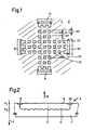
- Fig. 1 the layout of the mask 2 is shown with dashed lines, which during the implantation of the Electrodes 8-11 are used.
- the windows 12 of the mask 1, which are adjacent to the windows 13, are connected to each other to form a larger window 12 ', so that during manufacture within possible misalignment between the masks 1 and 2 of certain tolerance limits causes small offset errors.
- the invention can be used not only for increasing the sensitivity of an electronic chip use integrated Hall element.
- the invention can also be used to point to the same To produce chip n wells of different conductivity, which e.g. as resistors with different Resistance value can be used.
- the windows 12 are in the form of slots.
- the width S of the slots is smaller than the depth x 2 that the n-well 6 reaches in the subsequent diffusions.
- the windows in the implantation mask 2 which are provided for the doping of the electrodes 8-11 are shown with dashed lines.
- the distance D of the slots is approximately one to two times the depth x 2 . However, the distance D is chosen to be at most large enough that a single continuous n-well 6 is formed in the subsequent diffusions. The advantage here is that the effective dose Q eff is significantly smaller than the dose Q delivered by the implanter.
- FIG. 4 shows the layout of the mask 1 to be used in the implantation for a cross-shaped Hall element 3, which is formed by only two slots (window 12), the width S of which is substantially smaller than the depth x 2 .
Landscapes
- Physics & Mathematics (AREA)
- Condensed Matter Physics & Semiconductors (AREA)
- General Physics & Mathematics (AREA)
- Hall/Mr Elements (AREA)
Abstract
Bei der Herstellung von Halbleiterelementen wird üblicherweise durch Implantation und nachfolgende
Diffusion innerhalb eines Gebietes (7) eines ersten Leitfähigkeittyps ein zusammenhängendes Gebiet (6)
eines zweiten Leitfähigkeittyps gebildet wird. Erfindungsgemäss werden bei der Implantation
mindestens zwei voneinander getrennte Gebiete des zweiten Leitfähigkeittyps gebildet, deren Abstand
so bemessen ist, dass sich die mindestens zwei Gebiete bei der Diffusion zu dem zusammenhängenden
Gebiet vereinigen. Dank der Erfindung lassen sich Hallelemente (3) mit verbesserten Eigenschaften
ohne Prozessänderung auf einem Elektronikchip integrieren.
Description
Die Erfindung betrifft ein Verfahren zur Herstellung von Hallelementen der im Oberbegriff des
Anspruchs 1 genannten Art.The invention relates to a method for producing Hall elements in the preamble of
IC-Technologien sind optimiert für den einer Bausteinfamilie zugrundeliegenden Halbleiterschaltkreis.
Die CMOS Technologie beispielsweise ist optimiert zur Erzielung der besten Eigenschaften von MOS
Transistoren. Die Realisierung von Komponenten, z.B. von Sensoren, die nicht zur Standardreihe der
Bausteinfamilie gehören, ist daher nur möglich durch Eingehen von Kompromissen, die die Leistungsfähigkeit
dieser Komponente schmälern, oder durch Inkaufnahme erhöhter Kosten. Die Integration eines
als Magnetfeldsensor dienenden Hallelementes in einen CMOS Baustein z.B. ist auf drei Arten möglich:
Der Erfindung liegt die Aufgabe zugrunde, ein Verfahren zur Herstellung von Hallelementen anzugeben, bei dem sich das Hallelement auf demselben Chip befindet wie die Elektronik, ohne dass zusätzliche Prozessschritte erforderlich sind.The invention is based on the object of specifying a method for producing Hall elements, where the Hall element is on the same chip as the electronics, without additional Process steps are required.
Die Erfindung besteht in den im Anspruch 1 angegebenen Merkmalen. Vorteilhafte Ausgestaltungen
ergeben sich aus den abhängigen Ansprüchen.The invention consists in the features specified in
Bei der Herstellung von Halbleiterelementen wird üblicherweise durch Implantation und nachfolgende Diffusion innerhalb eines Gebietes eines ersten Leitfähigkeittyps ein zusammenhängendes Gebiet eines zweiten Leitfähigkeittyps gebildet. Form und Grösse des Gebietes des zweiten Leitfähigkeittyps ändern sich bei der nachfolgenden Diffusion nur in unbedeutendem Masse. Erfindungsgemäss wird nun bei der Implantation für das Gebiet des zweiten Leitfähigkeittyps eine Maske verwendet, bei der ein grösserer Teil der Fläche des Gebietes des zweiten Leitfähigkeittyps, die dieses Gebiet nach der nachfolgenden Diffusion bzw. den nachfolgenden Diffusionen einnimmt, abgedeckt ist. So ist es z.B. besonders vorteilhaft, bei der Implantation mindestens zwei voneinander getrennte Gebiete des zweiten Leitfähigkeittyps zu bilden, deren Abstand so bemessen ist, dass sich die mindestens zwei Gebiete bei der Diffusion zu dem zusammenhängenden Gebiet vereinigen. Die effektive Dichte der implantierten Ionen und damit der beweglichen Ladungsträger - Elektronen oder Löcher - lässt sich damit entsprechend dem Verhältnis von abgedeckter Fläche zur Gesamtfläche des Gebietes des zweiten Leitfähigkeittyps reduzieren. Dank der Erfindung lassen sich so beispielsweise Hallelemente ohne die oben genannten Nachteile auf einem Elektronikchip integrieren. Eine andere Möglichkeit zur Erhöhung der Empfindlichkeit eines Hallelementes, ohne eine Prozessänderung in Kauf nehmen zu müssen, besteht darin, bei der Implantation des später als magnetfeldempfindliche Zone dienenden Gebietes eine Maske mit zwei gekreuzt angeordneten Schlitzen zu verwenden, die sehr schmal im Vergleich zur Tiefe des Gebietes nach der Diffusion sind. Bei der Diffusion verbreitert sich das Gebiet des zweiten Leitfähigkeittyps infolge der seitlichen Diffusion sehr stark. Die effektive Ladungsträgerdichte, die die Empfindlichkeit des Hallelementes massgeblich bestimmt, wird somit bei der Diffusion wesentlich verkleinert.In the manufacture of semiconductor elements, usually by implantation and subsequent Diffusion within an area of a first conductivity type a contiguous area of a second conductivity type. Change the shape and size of the area of the second conductivity type diffuse only insignificantly in the subsequent diffusion. According to the invention, the Implantation for the area of the second conductivity type uses a mask in which a larger one Part of the area of the area of the second conductivity type that this area follows Diffusion or the subsequent diffusions is covered. So it is e.g. particularly advantageous during implantation, at least two areas of the second conductivity type which are separate from one another to form, whose distance is dimensioned so that the at least two areas in the diffusion to unite the contiguous area. The effective density of the implanted ions and thus the movable charge carriers - electrons or holes - can be calculated according to the ratio of Reduce the covered area to the total area of the area of the second conductivity type. thanks to the Invention, for example, Hall elements without the disadvantages mentioned above on one Integrate electronics chip. Another way to increase the sensitivity of a Hall element, without having to put up with a process change, consists of the implantation in the area that will later serve as a magnetic field sensitive zone, a mask with two crossed arranged to use slots that are very narrow compared to the depth of the area after the Are diffusion. In the case of diffusion, the area of the second conductivity type widens as a result of the lateral diffusion very strong. The effective charge carrier density, the sensitivity of the Hall element decisively determined, is thus significantly reduced during diffusion.
Nachfolgend werden Ausführungsbeispiele der Erfindung anhand der Zeichnung näher erläutert.Exemplary embodiments of the invention are explained in more detail below with reference to the drawing.
Es zeigen:
- Fig. 1
- Implantationsmasken für ein Hallelement,
- Fig. 2
- das Hallelement im Querschnitt, und
- Fig. 3, 4
- weitere Implantationsmasken für weitere Hallelemente.
- Fig. 1
- Implantation masks for a Hall element,
- Fig. 2
- the Hall element in cross section, and
- 3, 4
- further implantation masks for further Hall elements.
Der Beschreibung der Erfindung liegen die in der Herstellung von Halbleiterelementen geläufigen Begriffe zugrunde. Die Beschreibung beschränkt sich zudem auf die Darlegung der erfindungswesentlichen Merkmale.The description of the invention lies in those familiar in the production of semiconductor elements Terms. The description is also limited to the presentation of those essential to the invention Characteristics.
Die Fig. 1 zeigt in der Draufsicht das Layout von zwei Masken 1 und 2 für ein kreuzförmiges Hallelement,
die bei der Herstellung des Hallelementes als Implantationsmasken dienen. Die Fig. 2 zeigt das
fertige Hallelement 3 im Querschnitt. Das Hallelement 3 dient zur Messung eines seine Oberfläche 4 in
senkrechter Richtung durchflutenden Magnetfeldes B und ist beispielsweise in einer CMOS oder
Bipolar-Technologie hergestellt. Als Substrat dient ein Siliziumsubstrat 7 eines eines ersten Leitfähigkeittyps.
Das Hallelement 3 umfasst ein der Messung des Magnetfeldes B dienendes Gebiet 5, das als
Wanne 6 eines zweiten Leitfähigkeittyps im Siliziumsubstrat 7 realisiert ist, und vier Elektroden 8 - 11.
Über die vier Elektroden 8 - 11, die als hochdotierte Gebiete des zweiten Leitfähigkeittyps ausgebildet
sind, ist die Wanne 6 elektrisch kontaktiert. Die zwei einander gegenüberliegenden Elektroden 8 und 10
dienen als Stromkontakte zur Einspeisung eines Stromes I. Die Elektroden 9 und 11 dienen als
Spannungselektroden zum Abgreifen der sich zwischen ihnen bei Anwesenheit des Magnetfeldes B
einstellenden Hallspannung UH.1 shows a plan view of the layout of two
Die Hallspannung UH in Funktion des durch das Hallelement 3 fliessenden Stromes I und des
Magnetfeldes B und die strombezogene Empfindlichkeit SI des Hallelementes 3 sind gegeben durch
Die Wanne 6 ist bevorzugt eine n-dotierte Wanne, da die Beweglichkeit der Elektronen grösser als die
Beweglichkeit der Löcher ist. Für ein in einer Standard CMOS Technologie hergestelltes Hallelement
mit einer n-Wanne als magnetfeldempfindlichem Gebiet 5 erhält man mit G ≅ 0.7, rH ≅ 1.1,
q = 1.6*10-19 C und NS ≅ 8*1012 cm-2: SI ≅ 60 V/ATThe
Die n-Wanne 6 wird durch einen Implantations- und anschliessenden Diffusionsprozess hergestellt. Die
Grösse NS ist daher gleich der Anzahl der pro Flächeneinheit implantierten Ionen, der implantierten
Dosis Q.The n-
Die Erfindung besteht nun darin, für die Implantation einen vergleichsweise grossen Anteil der Oberfläche
der für das Hallelement 3 zu bildenden n-Wanne 6 abzudecken. Die für die Erstellung der n-Wanne
benützte Maske 1 (Fig. 1) weist deshalb beim Hallelement 3 nicht ein einziges grosses Fenster,
dessen Umriss der Form des Hallelementes 3 (Kreuzform in Fig. 1) entspricht, sondern eine Vielzahl
von kleinen Fenstern 12 auf. Die Abstände d1 zwischen den Fenstern 12 sind kleiner als die Tiefe x2, die
die n-Wanne 6 während des der Implantation folgenden Diffusionsprozesses (und allenfalls weiterer
Diffusionsprozesse) erreicht. Da der Abstand d1 zwischen den Fenstern 12 kleiner als die Distanz x2 ist,
bildet sich beim Diffusionsprozess infolge der auch seitlich erfolgenden Diffusion eine zusammenhängende
n-Wanne. Die kleinen Fenster 12 sind, wie in der Fig. 1 dargestellt, derart matrixartig
nebeneinander angeordnet, dass sich bei der Diffusion als magnetfeldempfindliches Gebiet die
zusammenhängende n-Wanne 6 bildet.The invention now consists in covering a comparatively large proportion of the surface of the n-
Bei einer n-Wannen CMOS Technologie beträgt die Tiefe x2 der n-Wannen 6 beispielsweise etwa 1 - 2
µm. Mit quadratischen Fenstern 12, deren lineare Abmessungen d2 0.8µm betragen und deren gegenseitiger
Abstand d1 ebenfalls 0.8µm beträgt, lässt sich die in das Siliziumsubstrat 7 implantierte Dosis
um den Faktor 4 verringern, da während der Implantation gegenüber herkömmlichen Herstellungsverfahren
drei Viertel des magnetfeldempfindlichen Gebietes 5 des Hallelementes 3 abgedeckt sind. Die
effektiv wirksame Dosis Qeff ist also um einen Faktor 4 kleiner als die vom Implanter gelieferte Dosis Q.
Folglich ist die Dichte der freien Ladungsträger NS in der Wanne 6 auch um den Faktor 4 kleiner und die
strombezogene Empfindlichkeit SI des derart hergestellten Hallelementes 3 um etwa einen Faktor 4
grösser.In the case of an n-well CMOS technology, the depth x 2 of the n-well 6 is, for example, approximately 1 to 2 μm. With
Der Abstand d1 könnte auch etwas grösser als die Distanz x2 gewählt werden, da die seitliche Diffusion
ja immer von zwei benachbarten Fenstern 12 ausgeht, wobei sich die Diffusionsfronten in der Mitte
zwischen den Fenstern 12 treffen und damit den elektrischen Zusammenschluss zu einer einzigen n-Wanne
6 bewirken. The distance d 1 could also be chosen somewhat larger than the distance x 2 , since the lateral diffusion always starts from two neighboring
Durch das gezielte Ausnutzen der seitlichen Diffusion kann somit ohne zusätzliche Prozessschritte ein Hallelement hoher Empfindlichkeit und die für den Betrieb des Hallelementes erforderliche Elektronik auf dem gleichen Chip realisiert werden.Through the targeted use of the lateral diffusion, one can therefore do without additional process steps Hall element with high sensitivity and the electronics required to operate the Hall element can be realized on the same chip.
In der Fig. 1 ist mit gestrichelten Linien das Layout der Maske 2 dargestellt, die bei der Implantation der
Elektroden 8 - 11 benutzt wird. Die Fenster 12 der Maske 1, die den Fenstern 13 benachbart sind, sind
miteinander zu einem grösseren Fenster 12' verbunden, damit ein bei der Herstellung innerhalb
bestimmter Toleranzgrenzen vorkommendes Misalignment zwischen den Masken 1 und 2 möglichst
geringe Offsetfehler verursacht.In Fig. 1, the layout of the
Die Erfindung lässt sich nicht nur für die Erhöhung der Empfindlichkeit eines im Elektronikchip integrierten Hallelementes benutzen. Die Erfindung kann auch benutzt werden, um auf dem gleichen Chip n-Wannen unterschiedlicher Leitfähigkeit herzustellen, die z.B. als Widerstände mit unterschiedlichem Widerstandswert verwendet werden können.The invention can be used not only for increasing the sensitivity of an electronic chip use integrated Hall element. The invention can also be used to point to the same To produce chip n wells of different conductivity, which e.g. as resistors with different Resistance value can be used.
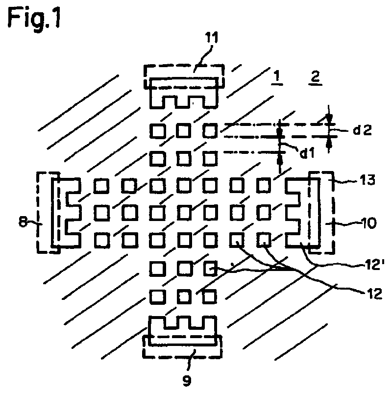
Die Fig. 3 zeigt das Layout der bei der Implantation zu verwendenden Masken 1 und 2 für ein weiteres
Hallelement 3. Bei der Maske 1, die für die Dotierung des magnetfeldempfindlichen Gebietes des Hallelementes
3, hier der n-Wanne 6 (Fig. 2), benutzt wird, weisen die Fenster 12 die Form von Schlitzen
auf. Die Breite S der Schlitze ist kleiner als die Tiefe x2, die die n-Wanne 6 bei den nachfolgenden
Diffusionen erreicht. Mit gestrichelten Linien sind die Fenster in der Implantationsmaske 2 dargestellt,
die für die Dotierung der Elektroden 8 - 11 vorgesehen sind. Der Abstand D der Schlitze beträgt etwa
das ein bis zweifache der Tiefe x2. Der Abstand D ist jedoch maximal so gross gewählt, dass sich bei
den nachfolgenden Diffusionen eine einzige zusammenhängende n-Wanne 6 bildet. Der Vorteil besteht
auch hier darin, dass die effektiv wirksame Dosis Qeff markant kleiner als die vom Implanter gelieferte
Dosis Q ist.3 shows the layout of the
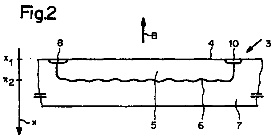
Die Fig. 4 zeigt das Layout der bei der Implantation zu verwendenden Maske 1 für ein kreuzförmiges
Hallelement 3, das durch nur zwei Schlitze (Fenster 12) gebildet ist, deren Breite S wesentlich kleiner
als die Tiefe x2 ist. Bei den nachfolgenden Diffusionsprozessen diffundieren die implantierten Ionen
sowohl in die Tiefe also auch in seitlicher Richtung, so dass die n-Wanne 6 schliesslich die Breite
Die Vorteile eines solchen Hallelementes sind:
- Die strombezogene Empfindlichkeit des Hallelementes SI erhöht sich gegenüber einem
konventionellen Hallelement, dessen n-Wanne um ein Vielfaches breiter als seine Tiefe x2 ist, um etwa
den Faktor

- Das magnetfeldempfindliche Volumen des Hallelementes wird äusserst klein, so dass das Magnetfeld mit hoher örtlicher Auflösung gemessen werden kann.
- The current-related sensitivity of the Hall element S I increases by about a factor compared to a conventional Hall element whose n-well is many times wider than its depth x 2
- The volume of the Hall element that is sensitive to magnetic fields becomes extremely small, so that the magnetic field can be measured with high local resolution.
Claims (4)
Applications Claiming Priority (4)
| Application Number | Priority Date | Filing Date | Title |
|---|---|---|---|
| CH17499 | 1999-02-01 | ||
| CH174992000 | 1999-02-01 | ||
| CH194099 | 1999-10-21 | ||
| CH194099 | 1999-10-21 |
Publications (2)
| Publication Number | Publication Date |
|---|---|
| EP1045461A2 true EP1045461A2 (en) | 2000-10-18 |
| EP1045461A3 EP1045461A3 (en) | 2005-02-09 |
Family
ID=25683758
Family Applications (1)
| Application Number | Title | Priority Date | Filing Date |
|---|---|---|---|
| EP00810082A Withdrawn EP1045461A3 (en) | 1999-02-01 | 2000-01-28 | Method of making Hall-effect devices |
Country Status (1)
| Country | Link |
|---|---|
| EP (1) | EP1045461A3 (en) |
Family Cites Families (2)
| Publication number | Priority date | Publication date | Assignee | Title |
|---|---|---|---|---|
| SI9110476A (en) * | 1991-03-18 | 1996-02-29 | Iskra Stevci Ind Merilne In Up | Hall sensor in integrated CMOS circuit |
| US5300454A (en) * | 1992-11-24 | 1994-04-05 | Motorola, Inc. | Method for forming doped regions within a semiconductor substrate |
-
2000
- 2000-01-28 EP EP00810082A patent/EP1045461A3/en not_active Withdrawn
Also Published As
| Publication number | Publication date |
|---|---|
| EP1045461A3 (en) | 2005-02-09 |
Similar Documents
| Publication | Publication Date | Title |
|---|---|---|
| DE3889245T2 (en) | Integrated and controlled power MOSFET. | |
| DE69128566T2 (en) | Composite integrated circuit arrangement | |
| DE2214935C2 (en) | Integrated MOS circuit | |
| DE69835183T2 (en) | Use of a camouflaged circuit | |
| DE4112072C2 (en) | MIS transistor with high withstand voltage and method for its production | |
| DE102014212651B4 (en) | Resistance element with specific piezoresistance coefficient, stress-compensated sensor system and method | |
| DE1614373C2 (en) | ||
| DE19501557C2 (en) | CMOS semiconductor device and method of manufacturing the same | |
| DE69327556T2 (en) | Method of manufacturing a dynamic semiconductor sensor with a thin thickness structure | |
| DE2655400A1 (en) | Semiconductor device and process for its production | |
| DE2242026A1 (en) | MIS FIELD EFFECT TRANSISTOR | |
| EP2503612A2 (en) | Vertical hall sensor and method of making a vertical hall sensor | |
| DE69518571T2 (en) | Protection arrangement against electrostatic discharge | |
| DE2342637A1 (en) | ZENER DIODE WITH THREE ELECTRICAL CONNECTION AREAS | |
| DE3714790A1 (en) | ZENER DIODE UNDER THE SURFACE AND MANUFACTURING METHOD | |
| DE19733974A1 (en) | MOSFET structure with first conductivity-type semiconductor substrate | |
| DE10224003B4 (en) | Semiconductor device and method for its manufacture | |
| DE1808928A1 (en) | Semiconductor component and method for its manufacture | |
| DE69117988T2 (en) | Semiconductor device with charge transfer device, MOSFETs and bipolar transistors - all formed in a single semiconductor substrate | |
| DE19710233A1 (en) | Semiconductor device, e.g. MOS transistor with CMOS structure | |
| DE2953394C2 (en) | ||
| DE10109174A1 (en) | Method for designing the structure of semiconductor integrated circuits and device for carrying out the same | |
| DE3119288A1 (en) | SEMICONDUCTOR ARRANGEMENT | |
| DE3842749A1 (en) | METHOD FOR PRODUCING AN INTEGRATED CIRCUIT | |
| DE10247431A1 (en) | Semiconductor device |
Legal Events
| Date | Code | Title | Description |
|---|---|---|---|
| PUAI | Public reference made under article 153(3) epc to a published international application that has entered the european phase |
Free format text: ORIGINAL CODE: 0009012 |
|
| AK | Designated contracting states |
Kind code of ref document: A2 Designated state(s): AT BE CH CY DE DK ES FI FR GB GR IE IT LI LU MC NL PT SE |
|
| AX | Request for extension of the european patent |
Free format text: AL;LT;LV;MK;RO;SI |
|
| PUAL | Search report despatched |
Free format text: ORIGINAL CODE: 0009013 |
|
| AK | Designated contracting states |
Kind code of ref document: A3 Designated state(s): AT BE CH CY DE DK ES FI FR GB GR IE IT LI LU MC NL PT SE |
|
| AX | Request for extension of the european patent |
Extension state: AL LT LV MK RO SI |
|
| STAA | Information on the status of an ep patent application or granted ep patent |
Free format text: STATUS: THE APPLICATION HAS BEEN WITHDRAWN |
|
| 18W | Application withdrawn |
Effective date: 20050218 |