EP1045461A3 - Method of making Hall-effect devices - Google Patents
Method of making Hall-effect devices Download PDFInfo
- Publication number
- EP1045461A3 EP1045461A3 EP00810082A EP00810082A EP1045461A3 EP 1045461 A3 EP1045461 A3 EP 1045461A3 EP 00810082 A EP00810082 A EP 00810082A EP 00810082 A EP00810082 A EP 00810082A EP 1045461 A3 EP1045461 A3 EP 1045461A3
- Authority
- EP
- European Patent Office
- Prior art keywords
- conductivity type
- effect devices
- implantation
- region
- making hall
- Prior art date
- Legal status (The legal status is an assumption and is not a legal conclusion. Google has not performed a legal analysis and makes no representation as to the accuracy of the status listed.)
- Withdrawn
Links
- 238000004519 manufacturing process Methods 0.000 title abstract 2
- 230000005355 Hall effect Effects 0.000 title 1
- 238000009792 diffusion process Methods 0.000 abstract 2
- 238000002513 implantation Methods 0.000 abstract 2
- 238000000034 method Methods 0.000 abstract 1
- 239000004065 semiconductor Substances 0.000 abstract 1
Classifications
-
- G—PHYSICS
- G01—MEASURING; TESTING
- G01R—MEASURING ELECTRIC VARIABLES; MEASURING MAGNETIC VARIABLES
- G01R33/00—Arrangements or instruments for measuring magnetic variables
- G01R33/02—Measuring direction or magnitude of magnetic fields or magnetic flux
- G01R33/06—Measuring direction or magnitude of magnetic fields or magnetic flux using galvano-magnetic devices
- G01R33/07—Hall effect devices
Landscapes
- Physics & Mathematics (AREA)
- Condensed Matter Physics & Semiconductors (AREA)
- General Physics & Mathematics (AREA)
- Hall/Mr Elements (AREA)
Abstract
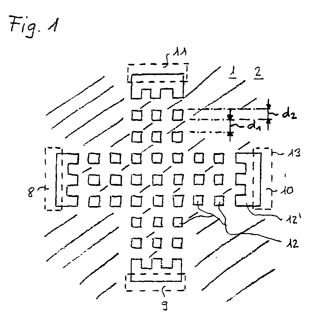
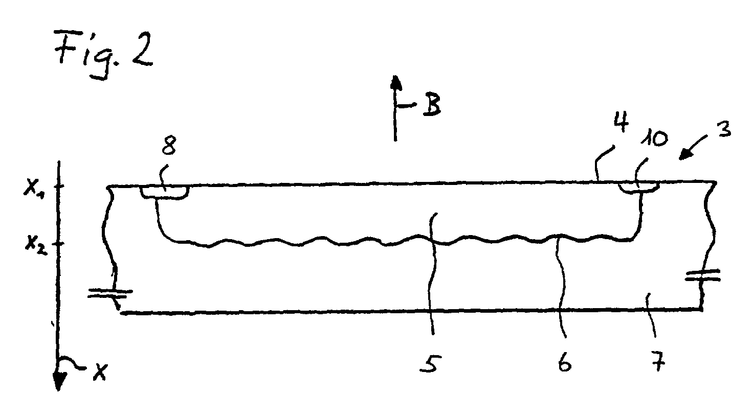
Bei der Herstellung von Halbleiterelementen wird üblicherweise durch Implantation und nachfolgende
Diffusion innerhalb eines Gebietes (7) eines ersten Leitfähigkeittyps ein zusammenhängendes Gebiet (6)
eines zweiten Leitfähigkeittyps gebildet wird. Erfindungsgemäss werden bei der Implantation
mindestens zwei voneinander getrennte Gebiete des zweiten Leitfähigkeittyps gebildet, deren Abstand
so bemessen ist, dass sich die mindestens zwei Gebiete bei der Diffusion zu dem zusammenhängenden
Gebiet vereinigen. Dank der Erfindung lassen sich Hallelemente (3) mit verbesserten Eigenschaften
ohne Prozessänderung auf einem Elektronikchip integrieren.
Applications Claiming Priority (4)
| Application Number | Priority Date | Filing Date | Title |
|---|---|---|---|
| CH174992000 | 1999-02-01 | ||
| CH17499 | 1999-02-01 | ||
| CH194099 | 1999-10-21 | ||
| CH194099 | 1999-10-21 |
Publications (2)
| Publication Number | Publication Date |
|---|---|
| EP1045461A2 EP1045461A2 (en) | 2000-10-18 |
| EP1045461A3 true EP1045461A3 (en) | 2005-02-09 |
Family
ID=25683758
Family Applications (1)
| Application Number | Title | Priority Date | Filing Date |
|---|---|---|---|
| EP00810082A Withdrawn EP1045461A3 (en) | 1999-02-01 | 2000-01-28 | Method of making Hall-effect devices |
Country Status (1)
| Country | Link |
|---|---|
| EP (1) | EP1045461A3 (en) |
Citations (2)
| Publication number | Priority date | Publication date | Assignee | Title |
|---|---|---|---|---|
| DE4208544A1 (en) * | 1991-03-18 | 1992-09-24 | Iskra Stevci Ind Merilne In Up | HALL SENSOR BUILT IN A CMOS INTEGRATED CIRCUIT |
| US5300454A (en) * | 1992-11-24 | 1994-04-05 | Motorola, Inc. | Method for forming doped regions within a semiconductor substrate |
-
2000
- 2000-01-28 EP EP00810082A patent/EP1045461A3/en not_active Withdrawn
Patent Citations (2)
| Publication number | Priority date | Publication date | Assignee | Title |
|---|---|---|---|---|
| DE4208544A1 (en) * | 1991-03-18 | 1992-09-24 | Iskra Stevci Ind Merilne In Up | HALL SENSOR BUILT IN A CMOS INTEGRATED CIRCUIT |
| US5300454A (en) * | 1992-11-24 | 1994-04-05 | Motorola, Inc. | Method for forming doped regions within a semiconductor substrate |
Non-Patent Citations (3)
| Title |
|---|
| JANOSSY B ET AL: "Hot carrier Hall devices in CMOS technology", SENSORS AND ACTUATORS A, ELSEVIER SCIENCE S.A., LAUSANNE, CH, vol. 71, no. 3, 1 December 1998 (1998-12-01), pages 172 - 178, XP004140091, ISSN: 0924-4247 * |
| STEINER R ET AL: "Fully packaged CMOS current monitor using lead-on-chip technology", 25 January 1998, IEEE PROCEEDINGS MEMS 98, THE ELEVENTH ANNUAL INTERNATIONAL WORKSHOP ON MICRO ELECTROMECHANICAL SYSTEMS, HEIDELBERG, GERMANY, 25-29 JAN. 1998, SEITEN 603-608, NEW YORK, USA, ISBN: 0-7803-4412-X, XP010270266 * |
| Z.RANDJELOVIC ET AL: "Low-Power High Sensitive CMOS Magnetic Field Hall Sensor", PROCEEDINGS OF THE EUROSENSORS XIII, 15B3, THE 13TH EUROPEAN CONFERENCE ON SOLID-STATE TRANSDUCERS, 12-15 SEPTEMBER 1999,THE HAGUE, NETHERLANDS, 1999, pages 601 - 604, XP002309855 * |
Also Published As
| Publication number | Publication date |
|---|---|
| EP1045461A2 (en) | 2000-10-18 |
Similar Documents
| Publication | Publication Date | Title |
|---|---|---|
| DE3110477C2 (en) | ||
| DE69226987T2 (en) | Local connections for integrated circuits | |
| AT502128A2 (en) | CONFIGURABLE INTEGRATED CIRCUIT WITH CAPACITOR GROUP USING VIA MASK LAYERS | |
| DE19542411C2 (en) | Semiconductor device and method of manufacturing the same | |
| DE1967363C2 (en) | ||
| EP0715344A3 (en) | Process for forming gate oxides possessing different thicknesses on a semiconductor substrate | |
| DE2153103A1 (en) | Integrated circuit arrangement and method of making the same | |
| DE10128577B4 (en) | Semiconductor pressure sensor with strain gauge and circuit section on a semiconductor substrate | |
| DE1918845A1 (en) | Process for the production of semiconductor components | |
| DE4320780B4 (en) | Semiconductor device and method of manufacture | |
| DE10297785T5 (en) | An electronics assembly having a denser contact assembly that allows lead routing to the contacts | |
| DE69029046T2 (en) | Contacts for semiconductor devices | |
| EP1187191A3 (en) | SOI substrate with semiconductor circuit therein and method of manufacturing same | |
| DE1589695A1 (en) | Method for manufacturing semiconductor components from a semiconductor board | |
| EP0390219A3 (en) | Semiconductor device and method of manufacturing the same | |
| DE19719272A1 (en) | Field insulation region in silicon substrate formation method for MOSFET formation | |
| DE1614575A1 (en) | Integrated circuit structure and method of making that structure | |
| DE4240565C2 (en) | Semiconductor device with a polysilicon resistance layer and method for producing the semiconductor device | |
| EP1045461A3 (en) | Method of making Hall-effect devices | |
| EP1336989A3 (en) | Transistor device | |
| DE19756409A1 (en) | Semiconductor component e.g. transistor production process | |
| US7592658B2 (en) | Method of forming a semiconductor device having a capacitor and a resistor | |
| DE3786693T2 (en) | Programmable contact pad. | |
| EP0973205A3 (en) | High voltage MOS transistor | |
| DE19512148C2 (en) | Method for producing a field oxide layer in a semiconductor device |
Legal Events
| Date | Code | Title | Description |
|---|---|---|---|
| PUAI | Public reference made under article 153(3) epc to a published international application that has entered the european phase |
Free format text: ORIGINAL CODE: 0009012 |
|
| AK | Designated contracting states |
Kind code of ref document: A2 Designated state(s): AT BE CH CY DE DK ES FI FR GB GR IE IT LI LU MC NL PT SE |
|
| AX | Request for extension of the european patent |
Free format text: AL;LT;LV;MK;RO;SI |
|
| PUAL | Search report despatched |
Free format text: ORIGINAL CODE: 0009013 |
|
| AK | Designated contracting states |
Kind code of ref document: A3 Designated state(s): AT BE CH CY DE DK ES FI FR GB GR IE IT LI LU MC NL PT SE |
|
| AX | Request for extension of the european patent |
Extension state: AL LT LV MK RO SI |
|
| STAA | Information on the status of an ep patent application or granted ep patent |
Free format text: STATUS: THE APPLICATION HAS BEEN WITHDRAWN |
|
| 18W | Application withdrawn |
Effective date: 20050218 |