EP1025565B1 - High speed memory self-timing circuitry and methods for implementing the same - Google Patents
High speed memory self-timing circuitry and methods for implementing the same Download PDFInfo
- Publication number
- EP1025565B1 EP1025565B1 EP98953641A EP98953641A EP1025565B1 EP 1025565 B1 EP1025565 B1 EP 1025565B1 EP 98953641 A EP98953641 A EP 98953641A EP 98953641 A EP98953641 A EP 98953641A EP 1025565 B1 EP1025565 B1 EP 1025565B1
- Authority
- EP
- European Patent Office
- Prior art keywords
- model
- wordline
- core
- circuit
- memory
- Prior art date
- Legal status (The legal status is an assumption and is not a legal conclusion. Google has not performed a legal analysis and makes no representation as to the accuracy of the status listed.)
- Expired - Lifetime
Links
- 238000000034 method Methods 0.000 title claims description 13
- 230000000630 rising effect Effects 0.000 claims description 13
- 230000001934 delay Effects 0.000 description 8
- 238000010586 diagram Methods 0.000 description 7
- 239000004065 semiconductor Substances 0.000 description 2
- XUIMIQQOPSSXEZ-UHFFFAOYSA-N Silicon Chemical compound [Si] XUIMIQQOPSSXEZ-UHFFFAOYSA-N 0.000 description 1
- 230000003321 amplification Effects 0.000 description 1
- 230000015572 biosynthetic process Effects 0.000 description 1
- 230000000295 complement effect Effects 0.000 description 1
- 230000008030 elimination Effects 0.000 description 1
- 238000003379 elimination reaction Methods 0.000 description 1
- 230000006870 function Effects 0.000 description 1
- 238000012986 modification Methods 0.000 description 1
- 230000004048 modification Effects 0.000 description 1
- 238000003199 nucleic acid amplification method Methods 0.000 description 1
- 238000011112 process operation Methods 0.000 description 1
- 229910052710 silicon Inorganic materials 0.000 description 1
- 239000010703 silicon Substances 0.000 description 1
- 239000000758 substrate Substances 0.000 description 1
- 238000003786 synthesis reaction Methods 0.000 description 1
- 230000001960 triggered effect Effects 0.000 description 1
Images


Classifications
-
- G—PHYSICS
- G11—INFORMATION STORAGE
- G11C—STATIC STORES
- G11C5/00—Details of stores covered by group G11C11/00
- G11C5/06—Arrangements for interconnecting storage elements electrically, e.g. by wiring
- G11C5/063—Voltage and signal distribution in integrated semi-conductor memory access lines, e.g. word-line, bit-line, cross-over resistance, propagation delay
-
- G—PHYSICS
- G11—INFORMATION STORAGE
- G11C—STATIC STORES
- G11C7/00—Arrangements for writing information into, or reading information out from, a digital store
- G11C7/10—Input/output [I/O] data interface arrangements, e.g. I/O data control circuits, I/O data buffers
- G11C7/1072—Input/output [I/O] data interface arrangements, e.g. I/O data control circuits, I/O data buffers for memories with random access ports synchronised on clock signal pulse trains, e.g. synchronous memories, self timed memories
-
- G—PHYSICS
- G11—INFORMATION STORAGE
- G11C—STATIC STORES
- G11C7/00—Arrangements for writing information into, or reading information out from, a digital store
- G11C7/14—Dummy cell management; Sense reference voltage generators
-
- G—PHYSICS
- G11—INFORMATION STORAGE
- G11C—STATIC STORES
- G11C8/00—Arrangements for selecting an address in a digital store
- G11C8/14—Word line organisation; Word line lay-out
Definitions
- the present invention relates generally to integrated circuits, and more particularly to methods and apparatus for improved memory self-timing circuitry.
- Semiconductor memory cores are usually laid-out in array format, such that each individual core cell is coupled by a wordline and a pair of differential bitlines.
- associated memory accessing circuitry is commonly designed around a memory core.
- some of the key memory accessing circuitry typically includes addressing circuitry for selecting a core cell, wordline drivers for driving a selected wordline, and sense amplifiers for amplifying the signal read from the selected core cell.
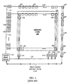
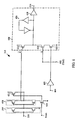
- Figure 1 shows a block diagram of a memory circuit having a memory core 100 and associated access circuitry.
- a plurality of core cells 102 are laid out in an array format throughout the memory core 100.
- a control block circuit 110 is used to control access to selected memory core cells 102 through the use of wordline drivers 106 and sense amplifiers (SA) 104.
- SA sense amplifiers
- control block circuit 110 is configured to produce a signal that triggers a selected wordline driver 106 upon a rising edge of the signal 116.
- the signal 116 experiences a falling edge (i.e. , at a time determined by a conventional self-timing architecture described below)
- the signal 116 will initiate the sensing of data through one of the selected sense amplifiers 104.
- the wordline drivers 106 are connected to each of the core cells 102 through the use of wordlines that interconnect each of the core cells 102 in a horizontal direction.
- the sense amplifiers 104 are connected to each of the core cells 102 in the vertical direction, through the use of differential bitlines.
- Self-timing architectures are generally used to approximate a standard delay time (i.e., which is generally the worst case timing delay for a given core) which will be used when an access to any one of the core cells 102 is attempted.
- the self-timing architecture is generally needed because the actual delay time of a particular core cell 102 will generally be different depending on the location of the particular core cell 102.
- a core cell 103 is located at the furthest location from a given wordline driver 106 and a given sense amplifier 104.
- an RC delay associated with the wordline that couples the wordline driver 106 to the core cell 103 and the RC delay associated with the bitlines that couple a sense amplifier 104 to the core cell 103, will have a combined RC delay that is larger than any other core cell 102 in the memory core 100.
- the combined RC delay of the wordline and the bitlines that couple to a core cell 101 will be smaller than any other core cell that is laid out in the memory core 100.
- the self-timing architecture which includes a model wordline driver 106', core cells 102', a model core cell 103', a model wordline 112a, model bitlines 112b, sense amplifier 104', and a self-timing return path 114 serves to establish the aforementioned standard delay time.
- the self-timing architecture is well suited to estimate when enough bitline differential has been achieved (i.e. , due to the worst case model core cell 103') to correctly perform a sense amplification to read the data of a given core cell 102 in the memory core 100.
- control block circuitry will initiate a select signal 116 to the model wordline driver 106' to access the model core cell 103'.
- a signal is passed through the model bitlines 112b, through sense amplifier 104' and along the self-timing return path 114, that communicates to the control block circuit 110.
- a particular problem with conventional self-timing architectures is that memory circuit will be ready to read data once the sense amplifier 104' has received the signal from the model core cell 103'.
- the additional self-timing return path 114 will necessarily add an additional RC delay to the RC delay of the model wordline 112a and the model bitline 112b.
- This additional RC delay introduced by the self-timing return path 114 will unfortunately slow down a memory accessing operation.
- the control block circuit 110 will not initiate a ready-to-read signal 116 to a given sense amplifier 104 until the control block circuit 110 receives the signal from the self-timing return path 114. Consequently, in applications where high-speed memory accessing is required, the performance of the entire memory circuit will suffer due to the additional RC delay introduced by the self-timing return path 114. below.
- EP 0 432 482 wherein the preamble of claim 1 is based discloses a RAM having a dummy word line with the same pattern and same gate as the word lines provided in RAM cells in order to detect that one of the word lines is selected until the end of the word lines, then operate a sense amplifier.
- the present invention fills these needs by providing methods and apparatuses for self-timing memory circuitry that eliminates unnecessary RC delays and substantially speeds up memory accessing operations. It should be appreciated that the present invention can be implemented in numerous ways, including as a process, an apparatus, a system, a device, or a method. Several embodiments of the present invention are described below.
- a memory circuit in one embodiment, includes a memory core having an array of core cells.
- the array of core cells are coupled to a plurality of wordlines and a plurality of bitline pairs.
- the memory circuit further includes a self-timing path that has a model core cell that is coupled to a model wordline, and the model wordline is driven by a model wordline driver.
- the self-timing path also includes a model sense amplifier that is coupled to the model core cell through a pair of model bitlines.
- the model wordline and the pair of model bitlines are each coupled to a plurality of dummy core cells to approximate an RC delay of a worst case core cell of the array of core cells.
- the model wordline is a folded wordline, such that the model wordline has a termination at a location that is proximate to the model wordline driver.
- a method for making a memory circuit with a self-timing path includes providing a memory core that has an array of core cells. The method further includes integrating a self-timing path of core cells along a model wordline and along a model pair of bitlines. The model wordline is folded such that a model core cell is placed substantially at a beginning point of the model wordline, and an ending point of the model wordline is coupled to the model core cell.
- Figure 1 shows a block diagram of a memory circuit having a memory core and associated access circuitry.
- Figure 2A shows a memory circuit having a memory core that includes an array of core cells in accordance with one embodiment of the present invention.
- FIGS. 2B and 2C show arrangements for a folded wordline in accordance with alternative embodiments of the present invention.
- Figure 3 shows an example of a model core cell in accordance with one embodiment of the present invention.
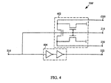
- Figure 4 is an example of a model wordline driver as shown in Figure 2A above in accordance with one embodiment of the present invention.
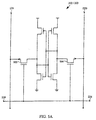
- Figure 5A shows an example of a core cell that lies in the memory core in accordance with one embodiment of the present invention.
- Figure 5B shows an example of a core cell that is laid out along the model bitlines in accordance with one embodiment of the present invention.
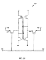
- Figure 5C shows an example of a core cell that is laid out along the model wordline in accordance with one embodiment of the present invention.
- Figure 6 is an example circuit diagram of a control circuit of Figure 2A in accordance with one embodiment of the present invention.
- Figure 7 shows a model path and read timing diagram 700 in accordance with one embodiment of the present invention.
- Figure 2A shows a memory circuit having a memory core 200 with an array of core cells 202 in accordance with one embodiment of the present invention.
- the core cells 202 are coupled to wordline drivers 206 through wordlines 226 in the horizontal direction, and sense amplifiers 204 through bitlines 229 in the vertical direction.
- Control circuitry 210 is also shown coupled to each of the wordline drivers 206 and the sense amplifiers 204.
- the sense amplifiers 204 are shown as discrete blocks, however, it should be understood that the sense amplifier is typically a circuit that is coupled to each of the bitlines 229 through well known Y-decoder circuitry (not shown).
- Y-decoders are used for addressing a selected column (i.e., differential bitlines) within the memory core 200.
- Y-decoders are generally implemented for reducing memory array aspect ratios by folding ( i.e. , dividing) long addressable memory columns into several shorter memory columns. Once folded into several columns, the Y-decoder is capable of accessing the addressed data by appropriately performing a suitable multiplexing function.
- an improved self-timing architecture is disclosed to eliminate delays associated with the self-timing return path 114 used in the conventional design of Figure 1. For example, once the RC delays of a wordline 222 and differential bitlines (i.e ., 230, /230) are rapidly transferred by a signal 214 to the control circuitry 210 (from a model sense amplifier 204'), a ready to read signal 216 will be immediately transmitted as shown in Figure 2A.
- the elimination of the RC delay associated with the self-timing return path of conventional designs is primarily facilitated by a folded wordline 220.
- the folded wordline 220 will include half of a set of core cells 202" stacked over the remaining half.
- This arrangement therefore provides an efficient path to connect the end of the wordline 222 to the model core cell 203', which is now arranged at the top-leftmost side of the memory core 200.
- the model bitlines 230 and /230 are interconnecting a set core cells 202' that lead to the model core cell 203'.
- the control circuitry 210 provides a wordline enable signal with a rising edge of the signal 216 to the model wordline driver 206'
- the RC delay is computed for only about the path traversed by the wordline 222 and the differential bitlines 230 and /230, that lead to the model sense amplifier 204'.
- the model sense signal 214 is provided to the control circuitry 210.
- the control circuitry 210 receives the signal 214, the control circuitry 210 will pass the falling edge of the ready to read signal 216 to the selected sense amplifiers 204.
- the self-timing architecture of the present invention provides a standard delay to be used by all of the core cells 202 and core cell 203 of the memory core 200. Further, the standard delay is preferably no worse than the RC delay for the worst case scenario of reading the core cell 203.
- Figure 2B shows another arrangement for the folded wordline 220' in accordance with an alternative embodiment of the present invention.
- the folded wordline 220' is arranged at a 90 degree angle compared to the folded wordline 220 of Figure 2A.
- This embodiment illustrates that the folded wordline 220' may be arranged in any manner that makes layout more suitable for a particular design, and need not be arranged in one horizontal orientation.
- Figure 2C shows yet another orientation for a folded wordline 220".
- the folded wordline 220" is laid out in an arrangement that would possibly make laying-out other miscellaneous logic more feasible in a particular integrated circuit design.
- the manner in which the folded wordline is arranged is not important, so long as the folded wordline provides a termination path of the wordline 222 substantially near the output of the model wordline driver 206'. When this is properly arranged, no excess RC delay is introduced in the self-timing path. Therefore, only the representative RC delay of the model wordline 222 and the model bitlines 230 and /230 are used by the control circuitry 210 to determine that a ready-to-read signal 216 should be provided to the given sense amplifiers 204.
- Figure 3 shows an example of a model core cell 203' in accordance with one embodiment of the present invention.
- a wordline 226 is shown as a line that does not interconnect with the model core cell 203', but leads directly into the core cells 202 that lie within the memory core 200.
- the model wordline 222 is shown coupled to a gate of transistors 302 and 304.
- the model bitline 230 which is connected to a terminal of transistor 304, and the complementary model bitline /230 that is connected to a terminal of transistor 302.
- signal 216 is provided by the control circuitry 210 to a gate of a transistor 306.
- the model core cell 203' is configured to perform a pull-down operation, which is configured to approximate the pull down strength of a core cell 202 that lies within the memory core 200.
- model core cell 203' may be finely tuned to increase its pull-down drive depending on the depth of a particular memory core 200.
- the model core cell 203' may be replaced by more than one model core cells to produce increased pull down strength, which may be useful to eliminate any delays that may be introduced by the control circuitry 210 or delays associated with driving larger memory cores.
- FIG 4 is an example of a model wordline driver 206' as shown in Figure 2A above in accordance with one embodiment of the present invention.
- the model wordline driver 206' is shown including a pre-charge circuit 402 that is coupled to the model bitlines 230 and /230, and the signal 216. Also shown is a buffer 404 that receives the signal 216 and outputs a buffered signal onto the model wordline 222.
- the model wordline driver 206' is triggered to commence an access operation.
- the buffer 404 is provided with sufficient delay to approximate the delay that will be experienced through a wordline drivers 206 that accesses the memory core 200, as shown in Figure 2A above.
- Figure 5A shows an example of a core cell 202 and 203 that lie in the memory core 200 in accordance with one embodiment of the present invention.
- the complimentary bitlines 229 and /229 are coupled to drain terminals of a pair of pass gate transistors 502 and 504, respectively.
- the wordline 226 is shown coupled to the gate of the pass gate transistors 502 and 504.
- one exemplary core cell 202/203 is shown, it should be understood that the embodiments of the present invention are applicable to other core cells and other memory circuits.
- the embodiment of the present invention may be applied to any number of memory circuits, such as ROM memory circuits, RAM memory circuits, SRAM memory circuits, DRAM memory circuits, EPROM memory circuits, EEPROM memory circuits, etc.
- memory circuits such as ROM memory circuits, RAM memory circuits, SRAM memory circuits, DRAM memory circuits, EPROM memory circuits, EEPROM memory circuits, etc.
- Figure 5B shows an example of a core cell 202' which is laid out along the model bitline in accordance with one embodiment of the present invention.
- bitline 230 is coupled to a drain terminal of a pass gate transistor 502'
- bitline /230 is coupled to a drain terminal of a pass gate transistor 504'.
- the gate of each of the pass gate transistors 502' and 504' are coupled to ground.
- Each of the core cells 202' are generally dummy core cells that are used to approximate the RC delay experienced on the bitlines 229' of the memory core 200.
- FIG. 5C shows an example of a core cell 202" which is laid out along the model wordline 222 in accordance with one embodiment of the present invention.
- a drain terminal of a pass gate transistor 502" is coupled to Vdd
- a drain terminal of a pass gate transistor 504" is coupled to Vdd.
- the gate of each of the pass gate transistors 502" and 504" are coupled to the model wordline 222.
- Each of the core cells 202" are also generally dummy core cells that are used to approximate the RC delay experienced on the wordline 226 of the memory core 200.
- FIG 6 is an example circuit diagram of the control circuitry 210 of Figure 2A in accordance with one embodiment of the present invention.
- the control circuitry 210 generally includes a model sense amplifier 204', and SET and RESET latch circuitry 606.
- the SET and RESET latch circuitry 606 generally includes a transistor 623 that is used for receiving a reset (/R) signal, a transistor 624 which is used for receiving a SET (S) signal from a clock (CLK) 602.
- the SET and RESET latch circuitry 606 also includes a transistor 622 that has its gate coupled to the output of a buffer 603, and the buffer 603 has an input 604 ( i.e., which is a delay of CLK 602).
- a latch 624 and an inverter 628 that produces the signal 216.
- a reset signal which is communicated to a gate of a transistor 620 and a gate of a transistor 621.
- bitline 230 is coupled to the model sense amplifier 204', which is shown to be an inverter circuit. The output of the model sense amplifier 204' is then coupled to an inverter 618.
- the reset signal is communicated after a falling edge of the signal 216 is received.
- signal 216 goes LOW (i.e., a falling edge)
- the sense amplifier is provided with a ready-to-read signal.
- signal 216 goes HI, a wordline driver is signaled to access a particular cell.
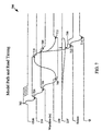
- Figure 7 shows a model path and read timing diagram 700 in accordance with one embodiment of the present invention.
- a memory clock (CLK) signal experiences a rising edge 702
- the signal 216 is caused to produce a rising edge 704.
- the rising edge 704 of signal 216 therefore causes all addressed wordlines (including the model wordline), to experience a rising edge 706.
- the rising edge 706 then causes the model bitline 230 to produce a falling edge 708.
- the falling edge 708 then causes a falling edge 710 in the signal 216.
- the falling edge 710 also acts to shut down the wordlines and model wordlines, open up the input latches, and pre-charges the bitline and data buses.
- the sense amplifier 204 when signal 216 experiences the falling edge 710, the sense amplifier 204 will be directed to begin a read, and therefore, cause the rising edge 712 on the sense line. More specifically, the falling edge 710 also produces a falling edge 709 for all of the address wordlines (including the model wordline), and a rising edge 711 in the bitline 230. In addition, the rising edge 712 of the sense signal will cause an edge 714 in an output "Q" reflecting the value of the sensed data, in this case a logical "1". It is important to note that the rising edge 712 will occur almost simultaneously when just enough bitline differential 730 has been achieved for the worst case core cell 203.
- the time in which the worst case core cell 203 reaches enough bitline differential is substantially the same as when the model core cell 203' has reached enough bitline differential.
- a memory circuit will be able to perform access operations at very high speeds because unnecessary delays have been eliminated.
- circuit diagrams may be embodied in any form which may include, for example, any suitable semiconductor substrate, printed circuit board, packaged integrated circuit, or software implementation.
- HDL design and synthesis programs such as, VHDL® hardware description language available from IEEE of New York, New York may be implemented to design the silicon-level layouts. Accordingly, the present embodiments are to be considered as illustrative and not restrictive, and the invention is not to be limited to the details given herein, but may be modified within the scope and equivalents of the appended claims.
Landscapes
- Engineering & Computer Science (AREA)
- Microelectronics & Electronic Packaging (AREA)
- Dram (AREA)
- Static Random-Access Memory (AREA)
- Read Only Memory (AREA)
Applications Claiming Priority (3)
| Application Number | Priority Date | Filing Date | Title |
|---|---|---|---|
| US959681 | 1992-10-13 | ||
| US08/956,981 US5999482A (en) | 1997-10-24 | 1997-10-24 | High speed memory self-timing circuitry and methods for implementing the same |
| PCT/US1998/021939 WO1999022376A1 (en) | 1997-10-24 | 1998-10-20 | High speed memory self-timing circuitry and methods for implementing the same |
Publications (3)
| Publication Number | Publication Date |
|---|---|
| EP1025565A1 EP1025565A1 (en) | 2000-08-09 |
| EP1025565A4 EP1025565A4 (en) | 2001-04-25 |
| EP1025565B1 true EP1025565B1 (en) | 2003-06-04 |
Family
ID=25498928
Family Applications (1)
| Application Number | Title | Priority Date | Filing Date |
|---|---|---|---|
| EP98953641A Expired - Lifetime EP1025565B1 (en) | 1997-10-24 | 1998-10-20 | High speed memory self-timing circuitry and methods for implementing the same |
Country Status (6)
| Country | Link |
|---|---|
| US (1) | US5999482A (enExample) |
| EP (1) | EP1025565B1 (enExample) |
| JP (1) | JP4209588B2 (enExample) |
| AU (1) | AU1096899A (enExample) |
| DE (1) | DE69815372T2 (enExample) |
| WO (1) | WO1999022376A1 (enExample) |
Families Citing this family (36)
| Publication number | Priority date | Publication date | Assignee | Title |
|---|---|---|---|---|
| US6016390A (en) * | 1998-01-29 | 2000-01-18 | Artisan Components, Inc. | Method and apparatus for eliminating bitline voltage offsets in memory devices |
| JP3548423B2 (ja) * | 1998-04-27 | 2004-07-28 | シャープ株式会社 | 半導体記憶装置 |
| US6629223B2 (en) * | 1998-10-06 | 2003-09-30 | Texas Instruments Incorporated | Method and apparatus for accessing a memory core multiple times in a single clock cycle |
| US6388931B1 (en) | 1999-02-25 | 2002-05-14 | Micron Technology, Inc. | Dummy wordline for controlling the timing of the firing of sense amplifiers in a memory device in relation to the firing of wordlines in the memory device |
| US6181626B1 (en) | 2000-04-03 | 2001-01-30 | Lsi Logic Corporation | Self-timing circuit for semiconductor memory devices |
| US6212117B1 (en) * | 2000-06-07 | 2001-04-03 | Hitachi Ltd. | Duplicate bitline self-time technique for reliable memory operation |
| US6222791B1 (en) * | 2000-06-15 | 2001-04-24 | Artisan Components, Inc. | Slew tolerant clock input buffer and a self-timed memory core thereof |
| JP4894095B2 (ja) * | 2001-06-15 | 2012-03-07 | 富士通セミコンダクター株式会社 | 半導体記憶装置 |
| JP4339532B2 (ja) * | 2001-07-25 | 2009-10-07 | 富士通マイクロエレクトロニクス株式会社 | セルフタイミング回路を有するスタティックメモリ |
| US6618309B2 (en) * | 2001-10-09 | 2003-09-09 | Analog Devices, Inc. | Adjustable memory self-timing circuit |
| US6730842B2 (en) * | 2001-12-19 | 2004-05-04 | Lsi Logic Corporation | Self-extraction panel hinge |
| US6980481B1 (en) * | 2001-12-20 | 2005-12-27 | Lsi Logic Corporatiion | Address transition detect control circuit for self timed asynchronous memories |
| JP2005025896A (ja) * | 2003-07-04 | 2005-01-27 | Sony Corp | 半導体記憶装置、および半導体記憶装置の読み出し方法 |
| US6891774B1 (en) | 2003-09-03 | 2005-05-10 | T-Ram, Inc. | Delay line and output clock generator using same |
| US7089439B1 (en) | 2003-09-03 | 2006-08-08 | T-Ram, Inc. | Architecture and method for output clock generation on a high speed memory device |
| US7464282B1 (en) | 2003-09-03 | 2008-12-09 | T-Ram Semiconductor, Inc. | Apparatus and method for producing dummy data and output clock generator using same |
| US6947349B1 (en) | 2003-09-03 | 2005-09-20 | T-Ram, Inc. | Apparatus and method for producing an output clock pulse and output clock generator using same |
| JP4050690B2 (ja) * | 2003-11-21 | 2008-02-20 | 株式会社東芝 | 半導体集積回路装置 |
| WO2005052944A1 (ja) * | 2003-11-28 | 2005-06-09 | Fujitsu Limited | セルフタイミング回路を有する半導体メモリ |
| US8116159B2 (en) * | 2005-03-30 | 2012-02-14 | Ovonyx, Inc. | Using a bit specific reference level to read a resistive memory |
| US7668029B2 (en) | 2006-08-11 | 2010-02-23 | Freescale Semiconductor, Inc | Memory having sense time of variable duration |
| US7518947B2 (en) * | 2006-09-28 | 2009-04-14 | Freescale Semiconductor, Inc. | Self-timed memory having common timing control circuit and method therefor |
| US7522461B2 (en) * | 2006-11-06 | 2009-04-21 | Infineon Technologies Flash Gmbh & Co. Kg | Memory device architecture and method for improved bitline pre-charge and wordline timing |
| DE102006054781A1 (de) * | 2006-11-21 | 2008-05-29 | Qimonda Flash Gmbh | Speichereinrichtung-Architektur und Verfahren zum verbesserten Bitleitung-Vorladen und Wortleitung-Timing |
| US7746716B2 (en) * | 2007-02-22 | 2010-06-29 | Freescale Semiconductor, Inc. | Memory having a dummy bitline for timing control |
| JP5000466B2 (ja) | 2007-11-28 | 2012-08-15 | イビデン株式会社 | 排気管 |
| US8233337B2 (en) * | 2009-10-19 | 2012-07-31 | International Business Machines Corporation | SRAM delay circuit that tracks bitcell characteristics |
| JP5539916B2 (ja) | 2011-03-04 | 2014-07-02 | ルネサスエレクトロニクス株式会社 | 半導体装置 |
| US9384790B2 (en) | 2012-07-30 | 2016-07-05 | Avago Technologies General Ip (Singapore) Pte. Ltd. | Memory device with separately controlled sense amplifiers |
| US8848414B2 (en) | 2012-10-22 | 2014-09-30 | International Business Machines Corporation | Memory system incorporating a circuit to generate a delay signal and an associated method of operating a memory system |
| US8730750B1 (en) | 2012-10-28 | 2014-05-20 | Lsi Corporation | Memory device with control circuitry for generating a reset signal in read and write modes of operation |
| JP5732575B2 (ja) * | 2014-05-01 | 2015-06-10 | ルネサスエレクトロニクス株式会社 | 半導体装置 |
| EP3204060A1 (en) * | 2014-10-07 | 2017-08-16 | Yissum Research Development Company of the Hebrew University of Jerusalem Ltd. | On-demand degradable medical devices |
| US9881687B2 (en) * | 2015-12-18 | 2018-01-30 | Texas Instruments Incorporated | Self-latch sense timing in a one-time-programmable memory architecture |
| US10156841B2 (en) | 2015-12-31 | 2018-12-18 | General Electric Company | Identity management and device enrollment in a cloud service |
| US9905315B1 (en) * | 2017-01-24 | 2018-02-27 | Nxp B.V. | Error-resilient memory device with row and/or column folding with redundant resources and repair method thereof |
Family Cites Families (25)
| Publication number | Priority date | Publication date | Assignee | Title |
|---|---|---|---|---|
| US4084240A (en) * | 1976-07-28 | 1978-04-11 | Chrysler Corporation | Mass production of electronic control units for engines |
| JPH07118196B2 (ja) * | 1988-12-28 | 1995-12-18 | 株式会社東芝 | スタティック型半導体メモリ |
| JPH0373495A (ja) * | 1989-02-15 | 1991-03-28 | Ricoh Co Ltd | 半導体メモリ装置 |
| US5146427A (en) * | 1989-08-30 | 1992-09-08 | Hitachi Ltd. | High speed semiconductor memory having a direct-bypass signal path |
| JPH03156795A (ja) * | 1989-11-15 | 1991-07-04 | Toshiba Micro Electron Kk | 半導体メモリ回路装置 |
| US5311471A (en) * | 1989-11-27 | 1994-05-10 | Kabushiki Kaisha Toshiba | Semiconductor memory device |
| JP2789779B2 (ja) * | 1990-04-14 | 1998-08-20 | 日本電気株式会社 | メモリ装置 |
| US5414663A (en) * | 1992-07-09 | 1995-05-09 | Creative Integrated Systems, Inc. | VLSI memory with an improved sense amplifier with dummy bit lines for modeling addressable bit lines |
| JP2530055B2 (ja) * | 1990-08-30 | 1996-09-04 | 株式会社東芝 | 半導体集積回路 |
| DE69026828T2 (de) * | 1990-12-13 | 1996-10-02 | Sgs Thomson Microelectronics | Verbesserte Abfühlschaltung für Speicheranordnungen, wie nichtflüchtige Speicher, mit verbesserter Abfühlunterscheidung |
| IT1253678B (it) * | 1991-07-31 | 1995-08-22 | St Microelectronics Srl | Architettura antirumore per memoria |
| US5677864A (en) * | 1993-03-23 | 1997-10-14 | Chung; David Siu Fu | Intelligent memory architecture |
| US5555521A (en) * | 1994-06-14 | 1996-09-10 | Sanyo Electric Co., Ltd | Method of operating the semiconductor memory storing analog data and analog data storing apparatus |
| KR0154193B1 (ko) * | 1994-12-30 | 1998-12-01 | 김주용 | 센스 앰프회로 |
| JP2643896B2 (ja) * | 1995-02-23 | 1997-08-20 | 日本電気株式会社 | 半導体メモリ |
| US5561629A (en) * | 1995-03-10 | 1996-10-01 | Xilinx, Inc. | Latching sense amplifier for a programmable logic device |
| JPH08273365A (ja) * | 1995-03-31 | 1996-10-18 | Nec Corp | 半導体記憶装置 |
| FR2734390B1 (fr) * | 1995-05-19 | 1997-06-13 | Sgs Thomson Microelectronics | Circuit de detection de courant pour la lecture d'une memoire en circuit integre |
| JPH0973776A (ja) * | 1995-09-07 | 1997-03-18 | Mitsubishi Electric Corp | 同期型半導体記憶装置 |
| US5636161A (en) * | 1995-10-30 | 1997-06-03 | Cypress Semiconductor Corporation | Eprom bit-line interface for implementing programming, verification and testing |
| TW307869B (en) * | 1995-12-20 | 1997-06-11 | Toshiba Co Ltd | Semiconductor memory |
| US5596539A (en) * | 1995-12-28 | 1997-01-21 | Lsi Logic Corporation | Method and apparatus for a low power self-timed memory control system |
| US5608681A (en) * | 1996-01-22 | 1997-03-04 | Lsi Logic Corporation | Fast memory sense system |
| DE69724327T2 (de) * | 1996-05-17 | 2004-06-17 | Hyundai Electronics America Inc., San Jose | Leistungsreduzierung während eines Blockschreibens |
| US5751649A (en) * | 1997-02-26 | 1998-05-12 | Artisan Components, Inc. | High speed memory output circuitry and methods for implementing same |
-
1997
- 1997-10-24 US US08/956,981 patent/US5999482A/en not_active Expired - Lifetime
-
1998
- 1998-10-20 AU AU10968/99A patent/AU1096899A/en not_active Abandoned
- 1998-10-20 DE DE69815372T patent/DE69815372T2/de not_active Expired - Lifetime
- 1998-10-20 WO PCT/US1998/021939 patent/WO1999022376A1/en not_active Ceased
- 1998-10-20 EP EP98953641A patent/EP1025565B1/en not_active Expired - Lifetime
- 1998-10-20 JP JP2000518387A patent/JP4209588B2/ja not_active Expired - Lifetime
Also Published As
| Publication number | Publication date |
|---|---|
| WO1999022376A1 (en) | 1999-05-06 |
| JP4209588B2 (ja) | 2009-01-14 |
| EP1025565A4 (en) | 2001-04-25 |
| US5999482A (en) | 1999-12-07 |
| EP1025565A1 (en) | 2000-08-09 |
| DE69815372T2 (de) | 2004-04-29 |
| DE69815372D1 (de) | 2003-07-10 |
| JP2001521262A (ja) | 2001-11-06 |
| AU1096899A (en) | 1999-05-17 |
Similar Documents
| Publication | Publication Date | Title |
|---|---|---|
| EP1025565B1 (en) | High speed memory self-timing circuitry and methods for implementing the same | |
| US6105106A (en) | Computer system, memory device and shift register including a balanced switching circuit with series connected transfer gates which are selectively clocked for fast switching times | |
| US6496420B2 (en) | Methods and apparatus for reading memory device register data | |
| KR100239958B1 (ko) | 반도체 기억장치 | |
| KR900005667B1 (ko) | 반도체 기억장치 | |
| KR0154586B1 (ko) | 반도체 기억장치 | |
| US5400274A (en) | Memory having looped global data lines for propagation delay matching | |
| US5341331A (en) | Data transmission circuit having common input/output lines | |
| US7161865B2 (en) | Semiconductor device | |
| US6038193A (en) | Single ended read scheme with segmented bitline of multi-port register file | |
| US6473357B1 (en) | Bitline/dataline short scheme to improve fall-through timing in a multi-port memory | |
| US20040136247A1 (en) | Sending signal through integrated circuit during setup time | |
| US6023428A (en) | Integrated circuit device having a memory array with segmented bit lines and method of operation | |
| EP0791932A2 (en) | Semiconductor memory device including main/sub-bit line arrangement | |
| WO2001043134A1 (en) | A sdram with a maskable input | |
| CN1637940B (zh) | 用于高速数据存取的半导体存储装置 | |
| US6072738A (en) | Cycle time reduction using an early precharge | |
| US5883854A (en) | Distributed balanced address detection and clock buffer circuitry and methods for making the same | |
| US6522564B2 (en) | Semiconductor memory device and signal line arrangement method thereof | |
| US6788615B2 (en) | System and method for low area self-timing in memory devices | |
| US5881008A (en) | Self adjusting pre-charge delay in memory circuits and methods for making the same | |
| JP2842816B2 (ja) | 半導体記憶装置 | |
| US6014338A (en) | Single ended read scheme with global bitline of multi-port register file | |
| US6072730A (en) | Low power differential signal transition techniques for use in memory devices | |
| US20040013025A1 (en) | Semiconductor memory device |
Legal Events
| Date | Code | Title | Description |
|---|---|---|---|
| PUAI | Public reference made under article 153(3) epc to a published international application that has entered the european phase |
Free format text: ORIGINAL CODE: 0009012 |
|
| 17P | Request for examination filed |
Effective date: 20000404 |
|
| AK | Designated contracting states |
Kind code of ref document: A1 Designated state(s): DE FR IT NL |
|
| RIN1 | Information on inventor provided before grant (corrected) |
Inventor name: BECKER, SCOTT, T. Inventor name: KORNACHUK, STEVE, P. |
|
| A4 | Supplementary search report drawn up and despatched |
Effective date: 20010308 |
|
| AK | Designated contracting states |
Kind code of ref document: A4 Designated state(s): DE FR IT NL |
|
| RIC1 | Information provided on ipc code assigned before grant |
Free format text: 7G 11C 7/14 A, 7G 11C 8/00 B |
|
| 17Q | First examination report despatched |
Effective date: 20020131 |
|
| GRAH | Despatch of communication of intention to grant a patent |
Free format text: ORIGINAL CODE: EPIDOS IGRA |
|
| GRAH | Despatch of communication of intention to grant a patent |
Free format text: ORIGINAL CODE: EPIDOS IGRA |
|
| GRAA | (expected) grant |
Free format text: ORIGINAL CODE: 0009210 |
|
| AK | Designated contracting states |
Designated state(s): DE FR IT NL |
|
| PG25 | Lapsed in a contracting state [announced via postgrant information from national office to epo] |
Ref country code: NL Free format text: LAPSE BECAUSE OF FAILURE TO SUBMIT A TRANSLATION OF THE DESCRIPTION OR TO PAY THE FEE WITHIN THE PRESCRIBED TIME-LIMIT Effective date: 20030604 Ref country code: IT Free format text: LAPSE BECAUSE OF FAILURE TO SUBMIT A TRANSLATION OF THE DESCRIPTION OR TO PAY THE FEE WITHIN THE PRESCRIBED TIME-LIMIT;WARNING: LAPSES OF ITALIAN PATENTS WITH EFFECTIVE DATE BEFORE 2007 MAY HAVE OCCURRED AT ANY TIME BEFORE 2007. THE CORRECT EFFECTIVE DATE MAY BE DIFFERENT FROM THE ONE RECORDED. Effective date: 20030604 |
|
| REF | Corresponds to: |
Ref document number: 69815372 Country of ref document: DE Date of ref document: 20030710 Kind code of ref document: P |
|
| NLV1 | Nl: lapsed or annulled due to failure to fulfill the requirements of art. 29p and 29m of the patents act | ||
| ET | Fr: translation filed | ||
| PLBE | No opposition filed within time limit |
Free format text: ORIGINAL CODE: 0009261 |
|
| STAA | Information on the status of an ep patent application or granted ep patent |
Free format text: STATUS: NO OPPOSITION FILED WITHIN TIME LIMIT |
|
| 26N | No opposition filed |
Effective date: 20040305 |
|
| REG | Reference to a national code |
Ref country code: FR Ref legal event code: TP Ref country code: FR Ref legal event code: CD |
|
| REG | Reference to a national code |
Ref country code: FR Ref legal event code: PLFP Year of fee payment: 18 |
|
| PGFP | Annual fee paid to national office [announced via postgrant information from national office to epo] |
Ref country code: FR Payment date: 20150908 Year of fee payment: 18 |
|
| PGFP | Annual fee paid to national office [announced via postgrant information from national office to epo] |
Ref country code: DE Payment date: 20151013 Year of fee payment: 18 |
|
| REG | Reference to a national code |
Ref country code: DE Ref legal event code: R119 Ref document number: 69815372 Country of ref document: DE |
|
| REG | Reference to a national code |
Ref country code: FR Ref legal event code: ST Effective date: 20170630 |
|
| PG25 | Lapsed in a contracting state [announced via postgrant information from national office to epo] |
Ref country code: DE Free format text: LAPSE BECAUSE OF NON-PAYMENT OF DUE FEES Effective date: 20170503 Ref country code: FR Free format text: LAPSE BECAUSE OF NON-PAYMENT OF DUE FEES Effective date: 20161102 |