EP1024366B1 - Testverfahren für Halbleiter und anisotroper Leiterfilm dazu - Google Patents
Testverfahren für Halbleiter und anisotroper Leiterfilm dazu Download PDFInfo
- Publication number
- EP1024366B1 EP1024366B1 EP00101568A EP00101568A EP1024366B1 EP 1024366 B1 EP1024366 B1 EP 1024366B1 EP 00101568 A EP00101568 A EP 00101568A EP 00101568 A EP00101568 A EP 00101568A EP 1024366 B1 EP1024366 B1 EP 1024366B1
- Authority
- EP
- European Patent Office
- Prior art keywords
- film
- film substrate
- semiconductor device
- conductive
- acf
- Prior art date
- Legal status (The legal status is an assumption and is not a legal conclusion. Google has not performed a legal analysis and makes no representation as to the accuracy of the status listed.)
- Expired - Lifetime
Links
- 239000004065 semiconductor Substances 0.000 title claims description 36
- 238000010998 test method Methods 0.000 title description 8
- 239000000758 substrate Substances 0.000 claims description 43
- 239000004020 conductor Substances 0.000 claims description 29
- 229910052751 metal Inorganic materials 0.000 claims description 27
- 239000002184 metal Substances 0.000 claims description 27
- 229920005989 resin Polymers 0.000 claims description 22
- 239000011347 resin Substances 0.000 claims description 22
- 238000011990 functional testing Methods 0.000 claims description 17
- 239000000463 material Substances 0.000 claims description 16
- 238000000034 method Methods 0.000 claims description 8
- 238000005311 autocorrelation function Methods 0.000 description 42
- 238000012360 testing method Methods 0.000 description 16
- RYGMFSIKBFXOCR-UHFFFAOYSA-N Copper Chemical compound [Cu] RYGMFSIKBFXOCR-UHFFFAOYSA-N 0.000 description 9
- 238000004519 manufacturing process Methods 0.000 description 9
- 239000010931 gold Substances 0.000 description 8
- PCHJSUWPFVWCPO-UHFFFAOYSA-N gold Chemical compound [Au] PCHJSUWPFVWCPO-UHFFFAOYSA-N 0.000 description 7
- 229910052737 gold Inorganic materials 0.000 description 7
- 239000010410 layer Substances 0.000 description 7
- PXHVJJICTQNCMI-UHFFFAOYSA-N Nickel Chemical compound [Ni] PXHVJJICTQNCMI-UHFFFAOYSA-N 0.000 description 4
- 238000011156 evaluation Methods 0.000 description 4
- 229910000679 solder Inorganic materials 0.000 description 3
- 229910052802 copper Inorganic materials 0.000 description 2
- 239000010949 copper Substances 0.000 description 2
- 230000002950 deficient Effects 0.000 description 2
- 239000007769 metal material Substances 0.000 description 2
- 229910052759 nickel Inorganic materials 0.000 description 2
- 230000000149 penetrating effect Effects 0.000 description 2
- 229920006122 polyamide resin Polymers 0.000 description 2
- 229920005992 thermoplastic resin Polymers 0.000 description 2
- 229920000178 Acrylic resin Polymers 0.000 description 1
- 239000004925 Acrylic resin Substances 0.000 description 1
- 239000004593 Epoxy Substances 0.000 description 1
- 239000004962 Polyamide-imide Substances 0.000 description 1
- 239000004697 Polyetherimide Substances 0.000 description 1
- 238000010521 absorption reaction Methods 0.000 description 1
- 239000000853 adhesive Substances 0.000 description 1
- 230000001070 adhesive effect Effects 0.000 description 1
- 229910052782 aluminium Inorganic materials 0.000 description 1
- XAGFODPZIPBFFR-UHFFFAOYSA-N aluminium Chemical compound [Al] XAGFODPZIPBFFR-UHFFFAOYSA-N 0.000 description 1
- 230000015572 biosynthetic process Effects 0.000 description 1
- 238000004364 calculation method Methods 0.000 description 1
- 239000011248 coating agent Substances 0.000 description 1
- 239000011247 coating layer Substances 0.000 description 1
- 238000000576 coating method Methods 0.000 description 1
- 238000005260 corrosion Methods 0.000 description 1
- 230000007797 corrosion Effects 0.000 description 1
- 230000000694 effects Effects 0.000 description 1
- 230000005611 electricity Effects 0.000 description 1
- 239000003822 epoxy resin Substances 0.000 description 1
- NBVXSUQYWXRMNV-UHFFFAOYSA-N fluoromethane Chemical compound FC NBVXSUQYWXRMNV-UHFFFAOYSA-N 0.000 description 1
- 239000011521 glass Substances 0.000 description 1
- 230000012447 hatching Effects 0.000 description 1
- 239000011810 insulating material Substances 0.000 description 1
- 238000009413 insulation Methods 0.000 description 1
- 230000010354 integration Effects 0.000 description 1
- 238000005259 measurement Methods 0.000 description 1
- 150000002739 metals Chemical class 0.000 description 1
- 229920006287 phenoxy resin Polymers 0.000 description 1
- 239000013034 phenoxy resin Substances 0.000 description 1
- 238000007747 plating Methods 0.000 description 1
- 229920002312 polyamide-imide Polymers 0.000 description 1
- 229920000647 polyepoxide Polymers 0.000 description 1
- 229920001225 polyester resin Polymers 0.000 description 1
- 239000004645 polyester resin Substances 0.000 description 1
- 229920001601 polyetherimide Polymers 0.000 description 1
- 239000009719 polyimide resin Substances 0.000 description 1
- 229920005749 polyurethane resin Polymers 0.000 description 1
- 230000002123 temporal effect Effects 0.000 description 1
- 229920006259 thermoplastic polyimide Polymers 0.000 description 1
- 229920001187 thermosetting polymer Polymers 0.000 description 1
- 238000004804 winding Methods 0.000 description 1
Images

Classifications
-
- G—PHYSICS
- G01—MEASURING; TESTING
- G01R—MEASURING ELECTRIC VARIABLES; MEASURING MAGNETIC VARIABLES
- G01R1/00—Details of instruments or arrangements of the types included in groups G01R5/00 - G01R13/00 and G01R31/00
- G01R1/02—General constructional details
- G01R1/04—Housings; Supporting members; Arrangements of terminals
- G01R1/0408—Test fixtures or contact fields; Connectors or connecting adaptors; Test clips; Test sockets
Definitions
- the present invention relates to an anisotropic conductive film. More particularly, the present invention relates to an anisotropic conductive film used to secure continuity of a bare chip semiconductor device during a functional test of the device, and to a test method for a bare chip semiconductor device using the film.
- One of the methods therefor includes bringing a semiconductor device into contact with a circuit board via an anisotropic conductive film at the same position as in actual mounting, and running a functional test of the device.
- the present inventors have closely examined the contact state during the test and found that bare chip semiconductor devices have warp, and the circuit boards have warp and waviness. As a result, many electrodes in one device fail to make an appropriate contact with the conductor part of the circuit board, which impairs the reliability of the test. To solve this problem, the contact load (pressure) may be increased. However, even if all the electrodes in the device and the conductor parts of the circuit board are connected, bump contacts formed on the electrodes of the device are deformed by the test itself. When the bare chip semiconductor device that passed the test is mounted on a circuit board, therefore, the deformed bump contacts now cause a . connection failure.
- the present invention provides the following.
- an anisotropic conductive film (hereinafter to be also referred to as "ACF") 1 is sandwiched between a bare chip semiconductor device 2 and a circuit board 3, and a contact load F is applied thereon to achieve functionally testable conduction between the device 2 and the board 3.
- ACF anisotropic conductive film
- the circuit board may be a product to mount a device or a model prepared for the test.
- the contact load should be within the range free from damaging the electrodes of a bare chip semiconductor device and achieve the lowest contact resistance.
- the electrodes to be subjected to the functional test may be a flat pad, a solder bump or other form and the contact load is preferably 29,4-490mN (3 - 50 gf), particularly 49-147mN (5 - 15 gf), per single electrode.
- the contact load is less than 29.4mN (3 gf)
- the connection becomes less certain (continuity does not reach 100%).
- it exceeds 490mN (50 gf) the electrode deforms during a test to cause connection failure upon mounting.
- a protrusion-like electrode such as a solder bump, a solder ball and the like having a protrusion height of approximately 20 ⁇ m - 200 ⁇ m, the effect of the above-mentioned range of contact load becomes most noticeable.
- the contact load per single electrode of a bare chip semiconductor device when, for example, a flip chip bonder is used can be obtained by dividing the total load by the number of electrodes brought into contact therewith.
- the contact load compresses ACF in the thickness direction.
- the device is tested for its function when the amount of deformation from the original thickness becomes 5 - 30 ⁇ m, thereby to allowing absorption of warp and waviness of the device or circuit board.
- the amount of deformation of ACF during a test can be directly measured.
- the elastic modulus of ACF is measured in advance and used for calculation using the contact load during the test.
- the elastic modulus of the entire structure of ACF should be set to 0.1 - 1.0 GPa (gigapascal) throughout the temperature range during the test of 25°C - 150°C. Particularly, 0.1 - 0.4 GPa is preferable.
- the elastic modulus is less than 0.1 GPa, even a small contact load produces strong adhesion, and in this case, the circuit board needs to be destroyed to save a good device.
- it exceeds 1.0 GPa waviness of circuit board and warp of chip cannot be absorbed and cause connection failure with a small contact load.
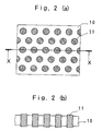
- ACF of the present invention comprises a number of conductive paths 11 made of a conductive material packed densely in a film substrate 10 made of an insulating resin.
- the conductive paths have a total length of 60 ⁇ m - 500 ⁇ m and the adjacent conductive paths are each insulated from the other.
- Each conductive path penetrates the film substrate in the thickness direction and both ends of the conductive path protrude from the film substrate.
- the ACF has an elastic modulus of 0.1 - 1.0 GPa at 25 - 150°C. The use of this film makes the test method of the present invention practical.
- the ACF of the present invention has a thickness equivalent to the length of a conductive path, which is 60 ⁇ m - 500 ⁇ m, practically preferably 60 ⁇ m - 200 ⁇ m.
- the thickness of a film substrate 10 is 30 ⁇ m -350 ⁇ m, particularly preferably 30 ⁇ m -150 ⁇ m.
- the height of protrusion of a conductive path from a film substrate is 10 ⁇ m - 80 ⁇ m, particularly 10 ⁇ m -50 ⁇ m.
- the insulating resin constituting the film substrate is exemplified by thermosetting resin, thermoplastic resin and the like.
- thermoplastic polyimide resin epoxy resin, polyetherimide resin, polyamide resin, phenoxy resin, acrylic resin, polycarbodiimide resin, fluorocarbon resin, polyester resin, polyurethane resin, polyamideimide resin and the like can be used according to the object.
- a thermoplastic resin is used. These resins may be used alone or in combination.
- a layer 12 made of a different material may be formed between the resin material of the film substrate 10 and the conductive path 11.
- This layer may have a multi-layer structure and may be made of any material appropriate to achieve a desired object of use and insulating property, conductivity and the like.
- a material highly adhesive to the resin material of the film substrate 10 may be used and a material having high heat resistance and high insulating property may be used for the layer 12 surrounding the conductive path 11.
- the conductive path may be made of a known conductive material. From the aspect of electrical property, preferred are metals such as copper, gold, aluminum, nickel and the like, and from the aspect of conductivity, preferred are copper and gold.
- the both ends protruding from the film surface may be further coated with a metal having high conductivity or high corrosion resistance, such as gold, nickel and the like.
- the shape and size of the section can be appropriately determined to meet the use of ACF of the present invention. It is preferably 5 ⁇ m - 30 ⁇ m in outer diameter to deal with a fine pitch (not more than 50 ⁇ m) electrode arrangement. As long as the above-mentioned range is satisfied, the shape of the section of the conductive path may be any, such as circle, polygon and the like.
- One electrode of a bare chip semiconductor device is preferably connected to one to three or so conductive paths.
- the conductive paths are preferably arranged densely in a film substrate.
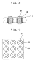
- the conductive paths when seen from the film plane preferably show a pattern as shown in Fig. 4 (a square), a densely-packed pattern as shown in Fig. 2(a), or other random patterns, with preference given to a highly dense pattern to deal with fine electrodes.
- the factors that determine the elastic modulus of the structure as a whole of ACF are the material of conductive path, section and total length of conductive path, density and arrangement pattern in film substrate, size of protrusion from film substrate, material of film substrate, thickness of film substrate and the like. These factors are appropriately determined to achieve an elastic modulus of the ACF structure as a whole of 0.1 - 1.0 GPa at 25 - 150°C.
- Such elastic modulus can be measured by a dynamic viscoelasticity measuring machine.
- the measurement conditions are: elongation in one direction of expansion of the film plane of ACF, constant wavelength, and 25°C and 150°C.
- the materials as exemplified above of the conductive path may show variation in the properties of conductivity, elastic modulus and the like for a single metal material, depending on how the conductive path is formed.
- the conductive path may be formed by plating a metal material in a through hole formed in a film substrate.
- the most preferable mode of formation in the present invention is penetrating a metal wire through a film substrate to give a conductive path.
- the above-mentioned metal conductor wires penetrating a film substrate can be obtained by fixing a number of insulating wires bundled densely in an inseparable manner and slicing the wires into a desired film thickness in the direction forming an angle with the insulating wires.
- the ACF of the present invention is most desirably prepared according to a production process including the following steps (1) to (4) or steps (1) to (3) and (5).
- the above-mentioned steps (1) to (3) enable the most efficient dense bundling of the insulating wires and easily produce the most dense collective pattern of the conductive paths, as shown in Fig. 2(a).
- the above-mentioned step (4) or (5) may be added depending on the process of protruding a conductive path.
- the production process it is also possible to form plural layers of a material on the surface of a metal conductor wire according to a desired use, such as for insulation, adhesion and the like.
- the ACF thus obtained shows variation in various electrical properties and mechanical properties, such as conductivity, dielectric property, insulating property, adhesiveness, strength and the like, in the direction of expansion of the film plane.
- the outer diameter of the metal conductor wire to be used in step (1) is preferably 5 - 30 ⁇ m for the functional test of a bare chip semiconductor device.
- sample 1 and sample 2 were prepared as ACF of the present invention by the production process including the steps (1) to (4) mentioned above and the following sample 3 and sample 4 for comparison.
- the method of the present invention was applied to examine the contact state and the like for judgement of the reliability of the test method.
- the ACF has a structure wherein a copper wire having a diameter of 18 ⁇ m penetrates a film substrate made of a polycarbodiimide resin to form a conductive path.
- the thickness of the film substrate was 50 ⁇ m, and the height of the copper wire protruding from each side of the film was 20 ⁇ m.
- the protrusion was gold plated in a thickness of 0.2 ⁇ m.
- the conductive paths were most densely packed as shown in Fig. 2(a) and the distance from one conductive path to the adjoining one as measured from the center line was 36 ⁇ m.
- the insulating wire used for winding in the above-mentioned step (1) was obtained by coating a polycarbodiimide resin on a 18 ⁇ m diameter copper wire.
- the elastic modulus of the structure as a whole of this ACF was 0.9 GPa.
- the basic structure, material, and production process were the same as in Sample 1.
- the conductive path had a diameter of 30 ⁇ m, the thickness of the film substrate was 50 ⁇ m, and the height of the copper wire protruding from each side of the film was 10 ⁇ m.
- the protrusion was gold plated in a thickness of 0.2 ⁇ m.
- the distance from one conductive path to the adjoining one as measured from the center line was 60 ⁇ m.
- the elastic modulus of the structure as a whole of this ACF was 0.5 GPa.
- the basic structure, material, and production process were the same as in Sample 1.
- the conductive path had a diameter of 18 ⁇ m, the thickness of the film substrate was 30 ⁇ m, and the height of the copper wire protruding from each side of the film was 10 ⁇ m.
- the protrusion was gold plated in a thickness of 0.2 ⁇ m.
- the distance from one conductive path to the adjoining one as measured from the center line was 36 ⁇ m.
- the elastic modulus of the structure as a whole of this ACF was 0.2 GPa at 25°C and 0.05 GPa at 150°C.
- the basic structure and production process were the same as in Sample 1.
- the elastic modulus of this ACF was 1.5 GPa, which was outside the range of ACF to be used in the present invention.
- the insulating material was a polyamide resin
- the conductive path had a diameter of 30 ⁇ m
- the thickness of the film substrate was 80 ⁇ m
- the amount of the copper wire protruding from each side of the film was 20 ⁇ m.
- the protrusion was gold plated in a thickness of 0.2 ⁇ m.
- the distance from one conductive path to the adjoining one as measured from the center line was 60 ⁇ m.
- the elastic modulus of the structure as a whole of this ACF was 1.5 GPa.
- the bare chip semiconductor device for evaluation was as follows. Chip size 10 mm ⁇ 10 mm, thickness 500 ⁇ m, electrode type: Au stud bump, electrode bump diameter 70 ⁇ m, bump height 70 ⁇ m, number of electrodes 156, center distance between electrodes 200 ⁇ m.
- the required numbers of the bare chip semiconductor devices and circuit boards for the above-mentioned evaluation were prepared.
- the ACFs of the above-mentioned Samples 1 to 4 were used to connect the bare chip semiconductor devices and circuit boards.
- a contact load was applied and the minimum load necessary for contact of all the electrodes of the bare chip semiconductor device was measured and taken as a contact load per one electrode.
- the contact load per one electrode was 196mN (20 gf) when all contact points were continued, which contact load was preferable.
- the deformation amount of ACF at that time was 15 ⁇ m, and ACF well absorbed warp and waviness of the bare chip semiconductor device and circuit board. Consequently, the functional test was confirmed to be highly reliable.
- the contact load per one electrode was 98mN (10 gf), which was preferable, and the deformation amount of ACF at that time was 7 ⁇ m.
- the contact load per one electrode was 98mN (10 gf), which was preferable, and the deformation amount of ACF at that time was 7 ⁇ m.
- warp and waviness of the bare chip semiconductor device and circuit board were absorbed well. Consequently, the functional test was confirmed to be highly reliable.
- the contact load per one electrode was 49mN (5 gf) when all contact points were continued, and the deformation amount of ACF at that time was 6 ⁇ m.
- the elastic modulus was set at 150°C to 0.05 GPa, the film substrate of ACF adhered to the semiconductor device and circuit board in the test at 150°C. As a result, the film was not easily released and inapplicable to a functional test.
- a bare chip semiconductor device and a circuit board can be connected at every contact point with the minimum load.
- the electrodes on the device and the conductor on the circuit board are not damaged, and a highly reliable functional test is available in a temporal connection state.
Landscapes
- Physics & Mathematics (AREA)
- General Physics & Mathematics (AREA)
- Measuring Leads Or Probes (AREA)
- Testing Or Measuring Of Semiconductors Or The Like (AREA)
- Wire Bonding (AREA)
- Non-Insulated Conductors (AREA)
- Testing Of Individual Semiconductor Devices (AREA)
Claims (5)
- Verfahren für einen Funktionstest eines Nacktchip-Halbleiterbauteils (2), umfassend die folgenden Schritte:wobei die anisotrop leitfähige Folie (1) ein Foliensubstrat (10) aus einem isolierenden Harz sowie mehrere leitfähige Bahnen (11), wobei jede Bahn eine Gesamtlänge von 60 bis 500 µm hat und aus einem leitfähigen Material besteht, umfasst und eine Struktur aufweist, bei der die mehreren leitfähigen Bahnen (11) das Foliensubstrat (10) in Richtung der Dicke durchdringen und aus der oberen und unteren Oberfläche des Foliensubstrats herausragen, wobei die Bahnen gegeneinander isoliert sind, wobei die Folie als Ganzes einen Elastizitätsmodul von 0,1 bis 1,0 GPa bei 25 bis 150 °C hat.(a) Einfügen einer anisotrop leitfähigen Folie (1) zwischen dem Nacktchip-Halbleiterbauteil (2) und einer Leiterplatte (3); und(b) Anlegen einer Kontaktlast von 29,4-490 mN (3-50 gf) pro Elektrode (2a) des Bauteils (2), so dass man eine Verformung der anisotrop leitfähigen Folie (1) von 5-30 µm und eine funktionstestfähige Leitung zwischen dem Bauteil (2) und der Platte (3) erreicht;
- Verfahren gemäß Anspruch 1, wobei wenigstens die leitfähigen Bahnen in dem Foliensubstrat metallisch leitende Drähte mit einem Durchmesser von 5 bis 30 µm sind und es sich bei dem, was herausragt, entweder um den metallisch leitenden Draht selbst oder ein auf einem Ende des metallisch leitenden Drahtes abgeschiedenes Metall handelt.
- Anisotrop leitfähige Folie (1) für einen Funktionstest eines Nacktchip-Halbleiterbauteils (2), die ein Foliensubstrat (10) aus einem isolierenden Harz sowie mehrere leitfähige Bahnen (11), wobei jede Bahn eine Gesamtlänge von 60 bis 500 µm hat und aus einem leitfähigen Material besteht, umfasst und eine Struktur aufweist, bei der die mehreren leitfähigen Bahnen (11) das Foliensubstrat (10) in Richtung der Dicke durchdringen und aus der oberen und unteren Oberfläche des Foliensubstrats herausragen, wobei die Bahnen gegeneinander isoliert sind, dadurch gekennzeichnet, dass die Folie als Ganzes einen Elastizitätsmodul von 0,1 bis 1,0 GPa bei 25 bis 150 °C hat.
- Folie gemäß Anspruch 3, wobei wenigstens die leitfähigen Bahnen (10) in dem Foliensubstrat metallisch leitende Drähte mit einem Durchmesser von 5 bis 30 µm sind und es sich bei dem, was herausragt, entweder um den metallisch leitenden Draht selbst oder ein auf einem Ende des metallisch leitenden Drahtes abgeschiedenes Metall handelt.
- Folie gemäß Anspruch 3, wobei wenigstens die leitfähigen Bahnen in dem Foliensubstrat mit einer Schicht bedeckt sind, die aus einem anderen Harzmaterial als dem Harzmaterial des Filmsubstrats besteht.
Applications Claiming Priority (2)
| Application Number | Priority Date | Filing Date | Title |
|---|---|---|---|
| JP02312899A JP3737899B2 (ja) | 1999-01-29 | 1999-01-29 | 半導体素子の検査方法およびそのための異方導電性フィルム |
| JP2312899 | 1999-01-29 |
Publications (2)
| Publication Number | Publication Date |
|---|---|
| EP1024366A1 EP1024366A1 (de) | 2000-08-02 |
| EP1024366B1 true EP1024366B1 (de) | 2003-06-11 |
Family
ID=12101895
Family Applications (1)
| Application Number | Title | Priority Date | Filing Date |
|---|---|---|---|
| EP00101568A Expired - Lifetime EP1024366B1 (de) | 1999-01-29 | 2000-01-27 | Testverfahren für Halbleiter und anisotroper Leiterfilm dazu |
Country Status (4)
| Country | Link |
|---|---|
| US (1) | US6597192B2 (de) |
| EP (1) | EP1024366B1 (de) |
| JP (1) | JP3737899B2 (de) |
| DE (1) | DE60003243T2 (de) |
Cited By (1)
| Publication number | Priority date | Publication date | Assignee | Title |
|---|---|---|---|---|
| CN100489548C (zh) * | 2003-10-14 | 2009-05-20 | Jsr株式会社 | 电路板检验装置 |
Families Citing this family (17)
| Publication number | Priority date | Publication date | Assignee | Title |
|---|---|---|---|---|
| US6471525B1 (en) * | 2000-08-24 | 2002-10-29 | High Connection Density, Inc. | Shielded carrier for land grid array connectors and a process for fabricating same |
| KR20030078870A (ko) * | 2000-12-08 | 2003-10-08 | 제이에스알 가부시끼가이샤 | 이방 도전성 시트 및 웨이퍼 검사 장치 |
| US6969622B1 (en) * | 2001-02-09 | 2005-11-29 | Jsr Corporation | Anisotropically conductive connector, its manufacture method and probe member |
| JP4522604B2 (ja) * | 2001-03-19 | 2010-08-11 | 日東電工株式会社 | 異方導電性フィルム |
| TW531868B (en) * | 2001-08-21 | 2003-05-11 | Au Optronics Corp | Soldering type anisotropic conductive film |
| US20040032271A1 (en) * | 2002-08-19 | 2004-02-19 | Blackwood Jeffrey E. | Anisotropic probing contactor |
| US20040079474A1 (en) * | 2002-10-24 | 2004-04-29 | Nitto Denko Corporation | Production method of anisotropic conductive connector |
| CN100359659C (zh) * | 2003-02-18 | 2008-01-02 | Jsr株式会社 | 各向异性导电连接器、探测部件和晶片检测设备以及晶片检测方法 |
| JP2004265728A (ja) | 2003-02-28 | 2004-09-24 | Jst Mfg Co Ltd | 誘電体シート |
| JP2005135772A (ja) * | 2003-10-30 | 2005-05-26 | Nitto Denko Corp | 異方導電性フィルムの製造方法 |
| KR100674938B1 (ko) * | 2005-01-12 | 2007-01-26 | 삼성전자주식회사 | 멀티칩 테스트용 프로브 카드 |
| TWI360182B (en) * | 2007-10-05 | 2012-03-11 | Ind Tech Res Inst | Method for making a conductive film |
| JP2009139298A (ja) * | 2007-12-10 | 2009-06-25 | Tokyo Electron Ltd | プローブカード |
| JP5664475B2 (ja) * | 2011-06-22 | 2015-02-04 | 株式会社デンソー | 半導体装置 |
| TWI462244B (zh) * | 2011-10-17 | 2014-11-21 | 財團法人工業技術研究院 | 異方向性導電膜片及其製作方法 |
| CN105305126A (zh) * | 2015-11-20 | 2016-02-03 | 华为技术有限公司 | 电连接器及通信设备 |
| US11637406B2 (en) * | 2017-05-18 | 2023-04-25 | Shin-Etsu Polymer Co., Ltd. | Electrical connector and method for producing same |
Family Cites Families (16)
| Publication number | Priority date | Publication date | Assignee | Title |
|---|---|---|---|---|
| JPS61292866A (ja) | 1985-06-21 | 1986-12-23 | 株式会社日立製作所 | 電子部品の接合方法 |
| US4924589A (en) * | 1988-05-16 | 1990-05-15 | Leedy Glenn J | Method of making and testing an integrated circuit |
| US5103557A (en) * | 1988-05-16 | 1992-04-14 | Leedy Glenn J | Making and testing an integrated circuit using high density probe points |
| US5716218A (en) * | 1991-06-04 | 1998-02-10 | Micron Technology, Inc. | Process for manufacturing an interconnect for testing a semiconductor die |
| US5323108A (en) * | 1992-01-23 | 1994-06-21 | Hewlett-Packard Company | Method for generating functional tests for printed circuit boards based on pattern matching of models |
| US5477160A (en) * | 1992-08-12 | 1995-12-19 | Fujitsu Limited | Module test card |
| EP0867942B1 (de) * | 1992-09-08 | 2002-04-24 | Seiko Epson Corporation | Flüssigkristallanzeigegerät |
| JPH07140209A (ja) * | 1993-09-20 | 1995-06-02 | Fujitsu Ltd | 回路配線基板の検査装置およびその検査方法 |
| JP3288840B2 (ja) * | 1994-02-28 | 2002-06-04 | 三菱電機株式会社 | 半導体装置およびその製造方法 |
| US6046598A (en) * | 1994-11-18 | 2000-04-04 | Fujitsu Limited | Test board and a test method using the same providing improved electrical connection |
| US5831441A (en) * | 1995-06-30 | 1998-11-03 | Fujitsu Limited | Test board for testing a semiconductor device, method of testing the semiconductor device, contact device, test method using the contact device, and test jig for testing the semiconductor device |
| US6245175B1 (en) * | 1996-08-08 | 2001-06-12 | Nitto Denko Corporation | Anisotropic conductive film and production method thereof |
| KR100467946B1 (ko) * | 1997-01-24 | 2005-01-24 | 로무 가부시키가이샤 | 반도체 칩의 제조방법 |
| US6049217A (en) * | 1997-12-30 | 2000-04-11 | Intel Corporation | Thermally enhanced test contactor |
| US5944093A (en) * | 1997-12-30 | 1999-08-31 | Intel Corporation | Pickup chuck with an integral heat pipe |
| JP2000286293A (ja) * | 1999-03-29 | 2000-10-13 | Nitto Denko Corp | 半導体装置および半導体素子実装用回路基板 |
-
1999
- 1999-01-29 JP JP02312899A patent/JP3737899B2/ja not_active Expired - Fee Related
-
2000
- 2000-01-27 EP EP00101568A patent/EP1024366B1/de not_active Expired - Lifetime
- 2000-01-27 DE DE60003243T patent/DE60003243T2/de not_active Expired - Lifetime
- 2000-01-31 US US09/494,379 patent/US6597192B2/en not_active Expired - Fee Related
Cited By (1)
| Publication number | Priority date | Publication date | Assignee | Title |
|---|---|---|---|---|
| CN100489548C (zh) * | 2003-10-14 | 2009-05-20 | Jsr株式会社 | 电路板检验装置 |
Also Published As
| Publication number | Publication date |
|---|---|
| DE60003243T2 (de) | 2004-04-08 |
| EP1024366A1 (de) | 2000-08-02 |
| HK1029832A1 (en) | 2001-04-12 |
| US6597192B2 (en) | 2003-07-22 |
| JP3737899B2 (ja) | 2006-01-25 |
| US20030080768A1 (en) | 2003-05-01 |
| DE60003243D1 (de) | 2003-07-17 |
| JP2000221209A (ja) | 2000-08-11 |
Similar Documents
| Publication | Publication Date | Title |
|---|---|---|
| EP1024366B1 (de) | Testverfahren für Halbleiter und anisotroper Leiterfilm dazu | |
| KR100248682B1 (ko) | 반도체 장치 및 반도체 칩 설치 방법 | |
| JP3578581B2 (ja) | ベアチップの実装構造および実装方法およびそれに用いるインターポーザ | |
| US20020063317A1 (en) | Tape carrier, semiconductor assembly, and semiconductor device, methods of manufacture thereof, and electronic instrument | |
| US5928458A (en) | Flip chip bonding with non conductive adhesive | |
| US20010040464A1 (en) | Electric contact device for testing semiconductor device | |
| JP2004534394A (ja) | 少なくとも1つの電子部品を備えた回路基板 | |
| US7231706B2 (en) | Method of manufacturing an anisotropic conductive film | |
| JP2002124319A (ja) | 異方導電性フィルムおよびそれを用いた半導体素子または電子部品の検査方法 | |
| JP4361161B2 (ja) | 異方導電性コネクター | |
| US6667542B2 (en) | Anisotropic conductive film-containing device | |
| HK1029832B (en) | Test method of semiconductor device and anisotropic conductive film therefor | |
| JP4256237B2 (ja) | 電子部品検査用の異方導電性フィルムおよびそれを用いた電子部品の検査方法 | |
| Palm et al. | Comparison of different flex materials in high density flip chip on flex applications | |
| US20230352387A1 (en) | Built-In Serial Via Chain for Integrity Monitoring of Laminate Substrate | |
| JPH06160433A (ja) | 回路基板検査用プローブおよびその製造方法 | |
| JP7287849B2 (ja) | 電気特性の検査冶具 | |
| JP2001004700A (ja) | インターポーザ基板 | |
| JPH05226430A (ja) | プローブカード構造体およびその製法 | |
| JP2001006770A (ja) | 異方導電性フィルム | |
| KR980013552A (ko) | 서로 마주보는 전극들을 상호접속하기 위한 접속시트 및 이 접속시트를 사용하는 전극 접속구조 및 접속방법 | |
| JP2733359B2 (ja) | テストヘッド構造 | |
| JPH07167912A (ja) | Lcd検査装置 | |
| JP2002228686A (ja) | 破損防止機能を有するコンタクトプローブ及びプローブ装置 | |
| JP2000294910A (ja) | 異方導電性フィルムの接合方法 |
Legal Events
| Date | Code | Title | Description |
|---|---|---|---|
| PUAI | Public reference made under article 153(3) epc to a published international application that has entered the european phase |
Free format text: ORIGINAL CODE: 0009012 |
|
| AK | Designated contracting states |
Kind code of ref document: A1 Designated state(s): DE GB |
|
| AX | Request for extension of the european patent |
Free format text: AL;LT;LV;MK;RO;SI |
|
| 17P | Request for examination filed |
Effective date: 20001124 |
|
| AKX | Designation fees paid |
Free format text: DE GB |
|
| 17Q | First examination report despatched |
Effective date: 20020522 |
|
| GRAH | Despatch of communication of intention to grant a patent |
Free format text: ORIGINAL CODE: EPIDOS IGRA |
|
| GRAH | Despatch of communication of intention to grant a patent |
Free format text: ORIGINAL CODE: EPIDOS IGRA |
|
| GRAA | (expected) grant |
Free format text: ORIGINAL CODE: 0009210 |
|
| AK | Designated contracting states |
Designated state(s): DE GB |
|
| REG | Reference to a national code |
Ref country code: GB Ref legal event code: FG4D |
|
| REF | Corresponds to: |
Ref document number: 60003243 Country of ref document: DE Date of ref document: 20030717 Kind code of ref document: P |
|
| PLBE | No opposition filed within time limit |
Free format text: ORIGINAL CODE: 0009261 |
|
| STAA | Information on the status of an ep patent application or granted ep patent |
Free format text: STATUS: NO OPPOSITION FILED WITHIN TIME LIMIT |
|
| 26N | No opposition filed |
Effective date: 20040312 |
|
| PGFP | Annual fee paid to national office [announced via postgrant information from national office to epo] |
Ref country code: GB Payment date: 20080123 Year of fee payment: 9 |
|
| GBPC | Gb: european patent ceased through non-payment of renewal fee |
Effective date: 20090127 |
|
| PG25 | Lapsed in a contracting state [announced via postgrant information from national office to epo] |
Ref country code: GB Free format text: LAPSE BECAUSE OF NON-PAYMENT OF DUE FEES Effective date: 20090127 |
|
| PGFP | Annual fee paid to national office [announced via postgrant information from national office to epo] |
Ref country code: DE Payment date: 20110119 Year of fee payment: 12 |
|
| PG25 | Lapsed in a contracting state [announced via postgrant information from national office to epo] |
Ref country code: DE Free format text: LAPSE BECAUSE OF NON-PAYMENT OF DUE FEES Effective date: 20120801 |
|
| REG | Reference to a national code |
Ref country code: DE Ref legal event code: R119 Ref document number: 60003243 Country of ref document: DE Effective date: 20120801 |