EP1015673B1 - Hitzeschildanordnung und verfahren zur züchtung silicium-einkristallen mit vielen leerstellen - Google Patents
Hitzeschildanordnung und verfahren zur züchtung silicium-einkristallen mit vielen leerstellen Download PDFInfo
- Publication number
- EP1015673B1 EP1015673B1 EP98937248A EP98937248A EP1015673B1 EP 1015673 B1 EP1015673 B1 EP 1015673B1 EP 98937248 A EP98937248 A EP 98937248A EP 98937248 A EP98937248 A EP 98937248A EP 1015673 B1 EP1015673 B1 EP 1015673B1
- Authority
- EP
- European Patent Office
- Prior art keywords
- heat shield
- crystal
- shield assembly
- assembly
- puller
- Prior art date
- Legal status (The legal status is an assumption and is not a legal conclusion. Google has not performed a legal analysis and makes no representation as to the accuracy of the status listed.)
- Expired - Lifetime
Links
- 238000000034 method Methods 0.000 title description 26
- 229910021421 monocrystalline silicon Inorganic materials 0.000 title description 11
- 239000013078 crystal Substances 0.000 claims description 141
- 230000033001 locomotion Effects 0.000 claims description 13
- 238000001816 cooling Methods 0.000 claims description 7
- 230000007547 defect Effects 0.000 description 31
- 239000000155 melt Substances 0.000 description 24
- 239000000463 material Substances 0.000 description 21
- XUIMIQQOPSSXEZ-UHFFFAOYSA-N Silicon Chemical compound [Si] XUIMIQQOPSSXEZ-UHFFFAOYSA-N 0.000 description 18
- 239000004065 semiconductor Substances 0.000 description 17
- 229910052710 silicon Inorganic materials 0.000 description 17
- 239000010703 silicon Substances 0.000 description 15
- 239000007787 solid Substances 0.000 description 13
- 230000002829 reductive effect Effects 0.000 description 11
- 235000012431 wafers Nutrition 0.000 description 10
- 238000010438 heat treatment Methods 0.000 description 9
- 229910021420 polycrystalline silicon Inorganic materials 0.000 description 5
- 230000015572 biosynthetic process Effects 0.000 description 4
- 230000008018 melting Effects 0.000 description 4
- 238000002844 melting Methods 0.000 description 4
- OKTJSMMVPCPJKN-UHFFFAOYSA-N Carbon Chemical compound [C] OKTJSMMVPCPJKN-UHFFFAOYSA-N 0.000 description 3
- 238000005054 agglomeration Methods 0.000 description 3
- 230000002776 aggregation Effects 0.000 description 3
- 230000008021 deposition Effects 0.000 description 3
- 229910002804 graphite Inorganic materials 0.000 description 3
- 239000010439 graphite Substances 0.000 description 3
- 230000002401 inhibitory effect Effects 0.000 description 3
- 238000002955 isolation Methods 0.000 description 3
- 238000004519 manufacturing process Methods 0.000 description 3
- 230000003647 oxidation Effects 0.000 description 3
- 238000007254 oxidation reaction Methods 0.000 description 3
- 238000007711 solidification Methods 0.000 description 3
- 230000008023 solidification Effects 0.000 description 3
- 238000010276 construction Methods 0.000 description 2
- 230000003247 decreasing effect Effects 0.000 description 2
- 230000006911 nucleation Effects 0.000 description 2
- 238000010899 nucleation Methods 0.000 description 2
- 230000036961 partial effect Effects 0.000 description 2
- 239000010453 quartz Substances 0.000 description 2
- 230000000979 retarding effect Effects 0.000 description 2
- HBMJWWWQQXIZIP-UHFFFAOYSA-N silicon carbide Chemical compound [Si+]#[C-] HBMJWWWQQXIZIP-UHFFFAOYSA-N 0.000 description 2
- 229910010271 silicon carbide Inorganic materials 0.000 description 2
- VYPSYNLAJGMNEJ-UHFFFAOYSA-N silicon dioxide Inorganic materials O=[Si]=O VYPSYNLAJGMNEJ-UHFFFAOYSA-N 0.000 description 2
- 238000010583 slow cooling Methods 0.000 description 2
- ZOKXTWBITQBERF-UHFFFAOYSA-N Molybdenum Chemical compound [Mo] ZOKXTWBITQBERF-UHFFFAOYSA-N 0.000 description 1
- 230000002411 adverse Effects 0.000 description 1
- 230000000295 complement effect Effects 0.000 description 1
- 239000000498 cooling water Substances 0.000 description 1
- 238000004033 diameter control Methods 0.000 description 1
- 238000004090 dissolution Methods 0.000 description 1
- 238000005516 engineering process Methods 0.000 description 1
- 238000000605 extraction Methods 0.000 description 1
- 239000012530 fluid Substances 0.000 description 1
- 239000012535 impurity Substances 0.000 description 1
- 238000009413 insulation Methods 0.000 description 1
- 229910052750 molybdenum Inorganic materials 0.000 description 1
- 239000011733 molybdenum Substances 0.000 description 1
- 229920005591 polysilicon Polymers 0.000 description 1
- 230000001737 promoting effect Effects 0.000 description 1
- 239000007858 starting material Substances 0.000 description 1
- 238000011282 treatment Methods 0.000 description 1
- XLYOFNOQVPJJNP-UHFFFAOYSA-N water Substances O XLYOFNOQVPJJNP-UHFFFAOYSA-N 0.000 description 1
Images

Classifications
-
- C—CHEMISTRY; METALLURGY
- C30—CRYSTAL GROWTH
- C30B—SINGLE-CRYSTAL GROWTH; UNIDIRECTIONAL SOLIDIFICATION OF EUTECTIC MATERIAL OR UNIDIRECTIONAL DEMIXING OF EUTECTOID MATERIAL; REFINING BY ZONE-MELTING OF MATERIAL; PRODUCTION OF A HOMOGENEOUS POLYCRYSTALLINE MATERIAL WITH DEFINED STRUCTURE; SINGLE CRYSTALS OR HOMOGENEOUS POLYCRYSTALLINE MATERIAL WITH DEFINED STRUCTURE; AFTER-TREATMENT OF SINGLE CRYSTALS OR A HOMOGENEOUS POLYCRYSTALLINE MATERIAL WITH DEFINED STRUCTURE; APPARATUS THEREFOR
- C30B29/00—Single crystals or homogeneous polycrystalline material with defined structure characterised by the material or by their shape
- C30B29/02—Elements
- C30B29/06—Silicon
-
- C—CHEMISTRY; METALLURGY
- C30—CRYSTAL GROWTH
- C30B—SINGLE-CRYSTAL GROWTH; UNIDIRECTIONAL SOLIDIFICATION OF EUTECTIC MATERIAL OR UNIDIRECTIONAL DEMIXING OF EUTECTOID MATERIAL; REFINING BY ZONE-MELTING OF MATERIAL; PRODUCTION OF A HOMOGENEOUS POLYCRYSTALLINE MATERIAL WITH DEFINED STRUCTURE; SINGLE CRYSTALS OR HOMOGENEOUS POLYCRYSTALLINE MATERIAL WITH DEFINED STRUCTURE; AFTER-TREATMENT OF SINGLE CRYSTALS OR A HOMOGENEOUS POLYCRYSTALLINE MATERIAL WITH DEFINED STRUCTURE; APPARATUS THEREFOR
- C30B15/00—Single-crystal growth by pulling from a melt, e.g. Czochralski method
- C30B15/14—Heating of the melt or the crystallised materials
-
- C—CHEMISTRY; METALLURGY
- C30—CRYSTAL GROWTH
- C30B—SINGLE-CRYSTAL GROWTH; UNIDIRECTIONAL SOLIDIFICATION OF EUTECTIC MATERIAL OR UNIDIRECTIONAL DEMIXING OF EUTECTOID MATERIAL; REFINING BY ZONE-MELTING OF MATERIAL; PRODUCTION OF A HOMOGENEOUS POLYCRYSTALLINE MATERIAL WITH DEFINED STRUCTURE; SINGLE CRYSTALS OR HOMOGENEOUS POLYCRYSTALLINE MATERIAL WITH DEFINED STRUCTURE; AFTER-TREATMENT OF SINGLE CRYSTALS OR A HOMOGENEOUS POLYCRYSTALLINE MATERIAL WITH DEFINED STRUCTURE; APPARATUS THEREFOR
- C30B15/00—Single-crystal growth by pulling from a melt, e.g. Czochralski method
- C30B15/20—Controlling or regulating
- C30B15/203—Controlling or regulating the relationship of pull rate (v) to axial thermal gradient (G)
-
- C—CHEMISTRY; METALLURGY
- C30—CRYSTAL GROWTH
- C30B—SINGLE-CRYSTAL GROWTH; UNIDIRECTIONAL SOLIDIFICATION OF EUTECTIC MATERIAL OR UNIDIRECTIONAL DEMIXING OF EUTECTOID MATERIAL; REFINING BY ZONE-MELTING OF MATERIAL; PRODUCTION OF A HOMOGENEOUS POLYCRYSTALLINE MATERIAL WITH DEFINED STRUCTURE; SINGLE CRYSTALS OR HOMOGENEOUS POLYCRYSTALLINE MATERIAL WITH DEFINED STRUCTURE; AFTER-TREATMENT OF SINGLE CRYSTALS OR A HOMOGENEOUS POLYCRYSTALLINE MATERIAL WITH DEFINED STRUCTURE; APPARATUS THEREFOR
- C30B15/00—Single-crystal growth by pulling from a melt, e.g. Czochralski method
- C30B15/20—Controlling or regulating
- C30B15/206—Controlling or regulating the thermal history of growing the ingot
-
- Y—GENERAL TAGGING OF NEW TECHNOLOGICAL DEVELOPMENTS; GENERAL TAGGING OF CROSS-SECTIONAL TECHNOLOGIES SPANNING OVER SEVERAL SECTIONS OF THE IPC; TECHNICAL SUBJECTS COVERED BY FORMER USPC CROSS-REFERENCE ART COLLECTIONS [XRACs] AND DIGESTS
- Y10—TECHNICAL SUBJECTS COVERED BY FORMER USPC
- Y10T—TECHNICAL SUBJECTS COVERED BY FORMER US CLASSIFICATION
- Y10T117/00—Single-crystal, oriented-crystal, and epitaxy growth processes; non-coating apparatus therefor
- Y10T117/10—Apparatus
- Y10T117/1024—Apparatus for crystallization from liquid or supercritical state
- Y10T117/1032—Seed pulling
-
- Y—GENERAL TAGGING OF NEW TECHNOLOGICAL DEVELOPMENTS; GENERAL TAGGING OF CROSS-SECTIONAL TECHNOLOGIES SPANNING OVER SEVERAL SECTIONS OF THE IPC; TECHNICAL SUBJECTS COVERED BY FORMER USPC CROSS-REFERENCE ART COLLECTIONS [XRACs] AND DIGESTS
- Y10—TECHNICAL SUBJECTS COVERED BY FORMER USPC
- Y10T—TECHNICAL SUBJECTS COVERED BY FORMER US CLASSIFICATION
- Y10T117/00—Single-crystal, oriented-crystal, and epitaxy growth processes; non-coating apparatus therefor
- Y10T117/10—Apparatus
- Y10T117/1024—Apparatus for crystallization from liquid or supercritical state
- Y10T117/1032—Seed pulling
- Y10T117/1068—Seed pulling including heating or cooling details [e.g., shield configuration]
Definitions
- the present invention relates generally to the production of semiconductor grade single crystal silicon used in the manufacture of electronic components, and more particularly to a heat shield assembly used in the growth of such semiconductor material.
- Single crystal silicon which is the starting material for most processes for the fabrication of semiconductor electronic components, is commonly prepared by the so-called Czochralski (“Cz”) method.
- the growth of the crystal is most commonly carried out in a crystal pulling furnace.
- polycrystalline silicon (“polysilicon”) is charged to a crucible and melted, a seed crystal is brought into contact with the molten silicon and a single crystal is grown by slow extraction. After formation of a neck is complete, the diameter of the crystal is enlarged by decreasing the pulling rate and/or the melt temperature until the desired or target diameter is reached.
- the cylindrical main body of the crystal which has an approximately constant diameter is then grown by controlling the pull rate and the melt temperature while compensating for the decreasing melt level.
- the crystal diameter must be reduced gradually to form an end-cone.
- the end-cone is formed by increasing the crystal pull rate and heat supplied to the crucible. When the diameter becomes small enough, the crystal is then separated from the melt.
- Silicon crystals grown from a melt are typically grown with an excess of one or the other type of intrinsic point defect, either crystal lattice vacancies or silicon self-interstitials. It is understood that the type and initial concentration of these point defects in the silicon, which become fixed at the time of solidification, are controlled by the ratio v/G 0 , where v is the growth velocity and G 0 is the instantaneous axial temperature gradient in the crystal at the time of solidification. As the value of v/G 0 exceeds a critical value, the concentration of vacancies increases. Likewise, as the value of v/G 0 falls below the critical value, the concentration of self-interstitials increases. Although neither form of defect is desirable, growth regimes which produce a predominance of vacancies are preferred, in general, by the semiconductor industry.
- Still another approach to dealing with the problem of agglomerated intrinsic point defects is the epitaxial deposition of a thin crystalline layer of silicon on the surface of a single crystal silicon wafer.
- the well known process of epitaxial deposition to acheive a more defect-free surface is described in Runyan, W.R. Semiconductor Integrated Surface Processing Technology , pp. 357-360 (Addison-Wesley Publishing Company, 1990). This process provides a single crystal silicon wafer having a surface which is substantially free of agglomerated intrinsic point defects. Epitaxial deposition, however, substantially increases the cost of the wafer.
- v/G 0 is controlled to be as high as possible.
- One way to increase the ratio is to increase the pull rate (growth velocity) of the crystal.
- the pull rate growth velocity
- the amount the pull rate may be increased.
- the other way to attack the problem is to reduce the thermal gradient G 0 in the crystal.
- a heat shield may be disposed within the crucible which conserves heat at the liquid-gas-solid interface, by forming a partial thermal cavity, the heat lost from the free melt surface.
- a collapsible heat shield disclosed in US-A-5,443,034 has an. upper shield fixed to the dome of the crystal puller.
- a lower heat shield is telescopingly received in the upper heat shield when the melt is being formed. The lower heat shield is extended during crystal growth.
- a heat shield assembly and method for a crystal puller which facilitates growth of high quality, low defect single crystals; the provision of such a heat shield assembly and method which inhibits agglomeration of defects in the crystal growth process; the provision of such a heat assembly and method which facilitates high throughput in the crystal puller; the provision of such a heat shield assembly and method which is capable of operating in confined space within a crystal puller; the provision of such a heat shield assembly and method which can be readily used in existing crystal pullers; the provision of such a heat shield assembly which can be raised and lowered using the existing pulling mechanism of the crystal puller; and the provision of such a heat shield assembly and method which is easy to use.
- the upper shield has connector means for connecting the heat shield assembly to a pulling mechanism of the crystal puller to raise and lower the heat shield assembly within the crystal puller.
- An intermediate heat shield has a central passage for receiving the crystal through the intermediate heat shield with the intermediate heat shield surrounding the crystal.
- the intermediate heat shield is constructed for engaging structure in the crystal puller to support the heat shield. assembly in the crystal puller.
- a lower heat shield has a central passage for receiving the crystal through the lower heat shield with the lower heat shield surrounding the crystal.
- the lower heat shield is connected to the upper heat shield for conjoint movement therewith and is slidingly and telescopingly received in the intermediate heat shield.
- the upper and lower heat shields are movable between a lower position in the crystal puller in which the lower shield is telescoped out of the intermediate heat shield and engages the intermediate heat shield for supporting the upper and lower heat shields, and a raised position in which the lower heat shield is telescoped upwardly into the intermediate heat shield and engages the intermediate heat shield for supporting the intermediate heat shield to move upwardly with the upper and lower heat shields.
- a method of growing vacancy rich single crystals comprises the steps of placing solid semiconductor source material in a crucible of a crystal puller and hanging a collapsible heat shield assembly on a pulling mechanism in the crystal puller above the crucible.
- the heat shield assembly as hung on the pulling mechanism is in a collapsed configuration.
- the solid semiconductor source material is heated to bring about melting of the source material.
- the heat shield assembly is lowered into engagement with support structure in the crystal puller generally above the crucible, the heat shield assembly assuming an extended position whereby a portion of the heat shield extends into the crucible in proximity to the surface of the molten semiconductor source material in the crucible.
- the heat shield assembly is disconnected from the pulling mechanism and a seed crystal is attached to the pulling mechanism.
- a seed crystal is lowered into contact with a melt of molten semiconductor source material in a crucible of a crystal puller and then raised from the melt so that semiconductor material from the melt freezes on the seed crystal to form a single crystal.
- Heat radiated from the side walls of the crucible is conserved with the heat shield assembly in a region adjacent the surface of the melt and located below the top of the crucible for inhibiting a high instantaneous axial thermal gradient in the single crystal in the region, whereby the single crystal has no vacancy/self-interstitial boundary ring or oxidation induced stacking fault ring.
- the single crystal is thermally shielded with the heat shield assembly at a location above the melt surface to slow cooling of the crystal in the range of approximately 1150°C to 1000°C whereby the single crystal has a predominance of vacancy defects and a low density of agglomerated vacancy defects.
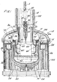
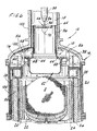
- a heat shield assembly constructed according to the principles of the present invention is generally indicated at 10.
- the heat shield assembly is preferably for use in a crystal puller, indicated generally at 12, of the type used to grow monocrystalline silicon ingots (e.g., ingot I of Fig. 1) according to the Czochralski method.
- the crystal puller 12 includes a shell (generally indicated at 14) for isolating an interior which includes a lower crystal growth chamber 16 and an upper pull chamber 18.
- the pull chamber has a smaller transverse dimension than the growth chamber.
- a quartz crucible 20 contains molten semiconductor source material M from which the monocrystalline silicon ingot I is grown.
- the crucible 20 includes a cylindrical side wall and is mounted on a turntable 22 for rotation about a vertical axis.
- the crucible 20 is also capable of being raised within the growth chamber 16 to maintain the surface of the molten source material M at the same level as the ingot I is grown and source material is removed from the melt.
- a heater includes generally vertically arranged heating panels 24 which are partially aligned with the side wall of the crucible 20.
- the heating panels 24 heat the crucible 20 and the interior of the crystal puller 12 to temperatures above the melting point of the source material (e.g., silicon).
- Insulation 26 is positioned to confine the heat to the interior of the shell 14.
- a pulling mechanism includes a pull shaft 29 extending down from a winch above the pull chamber 18.
- the crystal puller 12 may have a pull wire rather than a shaft, depending upon the type of puller.
- the pull shaft terminates in a seed crystal chuck 30 which holds a seed crystal 32 used to grow the monocrystalline ingot I.
- the pull shaft 29 has been partially broken away in Fig. 1 for clarity in illustration of a raised position of the seed chuck 30 and ingot I shown in phantom.
- the general construction and operation of the crystal puller 12, except to the extent explained more fully below, is well known to those of ordinary skill in the art and will not be further described.
- the heat shield assembly 10 of the present invention is employed during growth of the monocrystalline ingot I to control the heating and cooling of the ingot advantageously to produce a single crystal having fewer defects.
- the heat shield assembly 10 includes an upper heat shield 36 located above the crucible 20 which is free of engagement with the crystal puller shell 14.
- the upper heat shield 36 is generally tubular in shape, having a central passage for receiving the ingot I through the upper heat shield.
- the upper heat shield 36 preferably completely surrounds any portion of the ingot I received in the central passage and is interposed between the ingot I and the most closely adjacent interior walls of the shell 14. Heat transfer between the ingot I and the relatively cool interior walls of the shell is inhibited by the upper heat shield 36 for reducing the nucleation rate of agglomerated defects in the ingot within the upper heat shield above the crucible 20.
- a bottom heat shield of the heat shield assembly 10 is constructed to rest on an annular support structure 38 within the crystal puller shell 14 and to extend downwardly into the crucible 20.
- the bottom heat shield comprises an intermediate heat shield 40 and a lower heat shield 42 (both reference numbers designating their subjects generally).
- the intermediate heat shield 40 is generally tubular in shape and has a central passage for receiving the ingot I through the shield.
- the lower heat shield 42 is generally bowl shaped and has a central passage for receiving a portion of the ingot I into the lower heat shield.
- the lower edge margin of the lower heat shield 42 curves inwardly.
- the lower end of the lower heat shield 42 is spaced above the surface of the melt M in the lowest position of the heat shield assembly 10 for promoting heat transfer from the heating panels 24 through the side wall of the crucible 20 to the ingot I at the liquid-gas-solid interface at the surface of the melt.
- the lower heat shield 42 is made of a suitable material, such as silicon carbide coated graphite and includes a lower bowl portion and two arms 44 extending upwardly and inwardly from the top of the bowl portion to a collar 46. As best seen in Fig. 2, the arms 44 are located at circumferentially spaced positions at the top of the bowl portion so that the lower heat shield 42 is substantially open on its sides above the bowl portion. A lower edge margin of the upper heat shield 36 is received in the collar 46 and secured to the collar by suitable fasteners so that the upper and lower heat shields 36, 42 are rigidly connected together for conjoint movement.
- a suitable material such as silicon carbide coated graphite
- the intermediate heat shield 40 has a radially outwardly flaring annular lip 48 at its top edge margin.
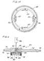
- the lip 48 has a shape complementary to the shape of four radially inwardly projecting tabs 50 (Fig. 1A) of the support structure 38, and rests on the tabs.
- the support structure 38 holds the intermediate heat shield 40 in a predetermined vertical location over the crucible 20 when the heat shield assembly 10 is in its operating position.
- the intermediate heat shield 40 extends downwardly into the crucible 20 a short distance.
- Guide/follower plates 52 are mounted on the intermediate heat shield 40 and received through respective openings in the lip 48 on opposite sides of the intermediate heat shield.
- the radially outer ends of the guide and follower plates 52 outside the intermediate heat shield 40 have notches 54 which receive portions of respective quartz guide posts 56 mounted on the support structure 38 in the crystal puller 12.
- the guide/follower plates 52 are capable of sliding along the height of the guide posts 56 so that the guide posts guide the heat shield assembly 10 as it is raised and lowered within the crystal puller 12.
- Guide pins 58 are received through holes in radially inner ends of respective guide/follower plates 52, through an arcuate cutout (not shown) in the lower heat shield and into a recess (not shown) in the intermediate heat shield 40.
- the guide pins 58 are free of fixed connection to the guide/follower plates 52, the intermediate heat shield 40 and the lower heat shield 42, but remain in fixed position relative to the intermediate shield in operation.
- the guide pins 58 guide motion of the upper and lower shields 36, 42 relative to the intermediate heat shield 40 between an extended position (Figs. 1) and a retracted position (Figs. 2 and 6).
- the lower heat shield 42 engages the guide/follower plates 52 so that any further upward movement by the upper and lower heat shields 36, 42 will result in conjoint upward movement by the intermediate heat shield 40.
- a lip 60 on the lower heat shield 42 rests on a lip 62 of the intermediate heat shield 40 so that no further downward movement of the upper and lower heat shields 36, 42 relative to the intermediate heat shield is permitted.
- the intermediate heat shield 40 supports the upper and lower heat shields 36, 42 in the extended position.
- the upper and lower heat shields 36, 42 are able to move relative to the intermediate heat shield 40 between the extended and retracted positions, with the lower heat shield sliding along and being guided by the guide pins 58.
- the upper heat shield 36 is made of silicon carbide coated graphite in a preferred embodiment, but may be made of other materials suitable for use in the environment of a crystal puller 12. For instance, it is contemplated that a multi-layered molybdenum construction (not shown) may be used in place of graphite.
- the upper heat shield 36 is operable to shield a portion of the ingot I having a temperature in the range of 1150°C to 1000°C from the relatively cool side walls of the crystal puller shell 14. Thus, heat transfer between the ingot I and the crystal puller 12 is reduced, and the number density of agglomerated defects in the ingot is reduced.
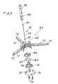
- the upper end of the upper heat shield 36 is formed with three, generally J-shaped slots 64 which permit a releasable, bayonet-type connection of a rotating hanger, generally indicated at 66, to the upper heat shield.
- the hanger 66 comprises a body 68 mounting three legs 70 projecting radially outwardly from the body at three equi-angularly spaced locations around the body.
- the legs 70 each have an end portion 72 of reduced diameter which is receivable in a corresponding one of the J-shaped slots 64 in the upper heat shield 36 to connect the hanger 66 to the upper heat shield.
- a mounting unit 74 is held in the body 68 by a retaining plate 76 attached by a pair of screws 78 to the body.
- the retaining plate 76 has a central axle 80 which is received in an opening (not shown) in the bottom of the mounting unit 74.
- a buffer plate 82 and ball bearings 84 are interposed within the body 68 between the mounting unit 74 and the body, permitting rotation of the body on the mounting unit.
- the pull shaft and seed crystal chuck 30 may rotate while the hanger 66 remains stationary.
- An adaptor 86 is constructed for mounting on the seed crystal chuck 30 in the same way as (and in place of) the seed crystal 32.
- the adaptor 86 has an internal, downwardly opening cavity accessible through a generally key-shaped opening 88 in one side of the adaptor.
- the larger portion of the opening 88 receives a ball end 90 of a connecting cable (generally indicated at 92) into the cavity.
- a narrower portion of the key-shaped opening 88 of the receives a thinner shank 94 of the cable 92 such that the ball end 90 is held in the cavity and the shank projects downwardly below the adaptor 86.
- the mounting unit 74 of the hanger 66 also has an internal cavity into which the cable 92 may pass through a key-shaped opening 96 accessible through an opening (not shown) in the body 68.
- An opposite ball end 98 of the cable 92 is received through the larger portion of the key-shaped opening 96 and into the mounting unit 74.
- the shank 94 of the cable 92 is received through a narrower portion of the opening 96 and projects upwardly out of the mounting unit 74 and the body 68. Once the ball end 98 enters the cavity, it is held in the mounting unit 74. In this way the hanger 66 is hung on the adaptor 86 and carried by the seed crystal chuck 30 and pull shaft.
- FIG. 1 An upper dome portion 100 and a pull chamber portion 102 of the crystal puller shell 14 are initially swung away from a growth chamber portion 104 of the shell, and solid polycrystalline silicon S is placed in the crucible 20.
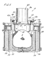
- the crystal puller 12 is illustrated with the dome and pull chamber portions 100, 102 swung away in Fig. 5.
- the crucible is in a lowered position.
- the solid silicon S is only schematically illustrated in the drawings, but may be conventional chunk or fluid bed polycrystalline silicon.
- the heating panels 24 in the crystal puller 12 are inactive and the interior of the crystal puller is open to the room.
- a number (three in the illustrated embodiment) of generally U-shaped supports 106 are placed on the support structure 38 in the crystal puller 12.
- the heat shield assembly 10 is then placed in the crystal growth chamber 16 so that the lip 48 of the intermediate heat shield 40 rests on the supports 106.
- the lower heat shield 42 is fully extended from the intermediate heat shield 40 so that the lip 60 of the lower heat shield rests on the lip 62 of the intermediate heat shield, and the upper and lower heat shields 36, 42 are supported by the intermediate heat shield.
- the dome and pull chamber portions 100, 102 of the shell 14 are then swung back over the crystal growth chamber portion 104 and heat shield assembly 10 is raised so that the upper heat shield 36 extends through the dome portion 100, out of the growth chamber 16 and into the pull chamber 18.
- the dome portion 100 is not seated on the growth chamber portion 104 of the shell 14, but rather is spaced slightly above the growth chamber.
- the pull chamber 18 is accessible through a door (not shown) in the side of the pull chamber portion 102 of the shell 14.
- the hanger 66 and adaptor 86 will have been pre-assembled by inserting the ball ends 90, 98 of the cable 92 through the key-shaped openings in the adaptor and mounting unit 74, respectively.
- the adaptor 86 is inserted into the chuck 30 and secured (such as by pinning in a conventional manner).
- the hanger 66 is lowered by lowering the pull shaft and guided so that each leg 70 is received in one of the J-shaped slots 64 in the upper heat shield 36.
- the hanger 66 is then turned so that the reduced diameter ends 72 of the legs align with smaller, toe ends 108 of the J-shaped slots 64.
- the winch is activated to raise the hanger 66 so that the reduced diameter ends 72 of the legs 70 are received in the toe ends 108 of the J-shaped slots 64 and the heat shield assembly 10 is raised off of the supports 106.
- the upper heat shield 36 and lower heat shield 42 initially move with the hanger, while the intermediate heat shield 40 remains stationary on the supports 106.
- the upper and lower heat shields 36, 42 are guided by guide pins 58 as the lower heat shield 42 telescopes partially into the intermediate heat shield 40.
- the lower heat shield 42 engages guide/follower plates 52 so that the intermediate heat shield 40 is now supported by the lower heat shield.
- the dome and pull chamber portions 100, 102 of the shell 14 are lowered down onto the growth chamber portion 104, as shown in Fig. 6.
- the winch is again activated to raise the heat shield assembly 10 up to the highest position.
- a limit switch (not shown) is provided in the growth chamber 16 to automatically shut off the winch when the heat shield assembly 10 is fully raised.
- the upper heat shield 36 is disposed within a necked down portion of the growth chamber 16, and also the pull chamber 18.
- the lower heat shield 42 is telescoped into the intermediate heat shield 40 so that the heat shield assembly 10 has a very small profile within the growth chamber 16.
- the crucible 20 is raised within the growth chamber 16 and a vacuum is drawn in the crystal puller 12.
- the heating panels 24 are activated to melt the solid polycrystalline silicon S in the crucible 20.
- the winch is activated to lower the heat shield assembly 10 down toward the crucible 20.
- the guide/follower plates 52 slide along the guide posts 56 to steady the motion of the heat shield assembly 10 as it moves downward.
- the lip 48 of the intermediate heat shield 40 engages the tabs 50 of the support structure 38, halting further downward movement of the intermediate heat shield.
- the upper and lower heat shields 36, 42 continue downwardly, with the lower heat shield sliding along guide pins 58. Once the lip 60 of the lower heat shield 62 engages the lip 62 of the intermediate heat shield 40, downward movement of the upper and lower heat shields 36, 42 is stopped.
- the upper and lower heat shields are supported by the intermediate heat shield 40, and the entire heat shield assembly 10 is located within the growth chamber 16.
- the hanger 66 is lowered further so that its legs 70 drop out of the narrow toe ends 108 of the J-shaped slots 64.
- the hanger 66 is then turned by operation of the winch so that the legs 70 are aligned with wider portions of the J-shaped slots 64, and the winch is activated to raise the hanger, disconnecting it from the upper heat shield 36.
- the hanger 66 may then be raised upward out of the growth chamber 16 and into the pull chamber 18.
- An isolation valve of the crystal puller 12 is closed, isolating the growth chamber 16 from the pull chamber 18 so that low pressure and high temperature conditions may be maintained in the growth chamber.
- the isolation valve between the growth chamber 16 and pull chamber 18 has not be shown in the drawings.
- the door of the pull chamber portion 102 is opened at the hanger 66 and adaptor 86 are removed from the seed crystal chuck 30.
- a seed crystal 32 is mounted in the chuck 30 and the door of the pull chamber portion 102 is closed.
- the isolation valve is opened and the winch activated to lower the seed crystal 32 down to the molten silicon M in the crucible 20.
- the winch is activated to withdraw the seed crystal upwardly.
- Silicon freezes on the seed crystal 32 in a monocrystalline structure, after the Czochralski method, forming the generally cylindrical ingot I (Fig. 1).
- the bottom edge of the lower heat shield 42 is preferably about 50-60 mm above the surface of the melt M in the crucible 20.
- the lower heat shield 42 prevents heat from radiating from the side walls of the crucible 20 to the ingot I except in the space between the bottom of the lower heat shield and the surface of the melt M.
- the heat shield assembly 10 is disposed between the ingot I at the cooler side walls of the shell 14, inhibiting heat transfer from the ingot. As a result, heat is conserved at the surface of the melt (i.e., the liquid-gas-solid interface), and increasing the temperature of the ingot I at the interface, thereby reducing the instantaneous axial temperature gradient G 0 in the ingot at the interface.
- an upper portion of the ingot I (shown in solid lines) has passed into the central passage of the lower heat shield 42. This portion of the ingot is shielded from the heat radiated from the side walls of the crucible 20. The portion of the ingot I in this higher position is also exposed to the opening spanned by the arms 44 between the upper and lower heat shields 36, 42. The portion of the ingot within the lower heat shield 42 now "sees" the cool side walls of the shell 14. Substantial heat transfer between the water cooled side walls of the shell 14 and the ingot I occurs and there is rapid cooling of the ingot within the lower heat shield 42.
- the ingot I continues to grow, and a portion enters the upper heat shield 36, as shown in phantom in Fig. 1.
- the upper heat shield 36 is interposed between the sides of the ingot and the side walls of the shell 14.
- the upper heat shield 36 is positioned so that the portions of the ingot I entering the upper heat shield are approximately at 1150°C.
- heat transfer from the ingot I to the side walls of the shell 14 is dramatically reduced so that the instantaneous temperature gradient G 0 is lessened in the portion of the ingot within the upper heat shield.
- the heat shield assembly 10 and crystal puller 12 of the present invention are achieved by the heat shield assembly 10 and crystal puller 12 of the present invention.
- the heat shield assembly 10 is compact and constructed for partial collapse as it is raised to minimize the space necessary to operate within the growth chamber 16.
- a high v/G 0 ratio is achieved at the liquid-gas-solid interface by reducing heat loss in the ingot I in the crucible 20 at the liquid-gas-solid interface.
- the gradient G 0 may be reduced from 22.84 °C / cm for unshielded Czochralski to 21.05 °C / cm using the heat shield assembly and method of the present invention.
- the ratio of v/G 0 may be increased from 0.000060 cm 2 /°C-sec to 0.000047 cm 2 /°C-sec. Accordingly, there is a predominance of crystal lattice vacancies everywhere in the crystal and no radial vacancy/self-interstitial boundary ring in the ingot I.
- the ratio v/G 0 is increased without changing the pull rate v.
- the pull rate profile of crystals pulled is not altered substantially from ordinary, unshielded Czochralski. However, it is to be understood that variation in the pull rate may be employed to increase the ratio v/G 0 .
- Rapid cooling of the ingot I is achieved within the lower heat shield 42 as is desirable by providing an opening between the upper and lower heat shields 36, 42.
- the ingot I is again shielded in the area where the ingot is between approximately 1150°C and 1000°C to reduce agglomeration of vacancies in the ingot.
- the temperature gradient in this region of the ingot I may be lowered from 14.1 °C / cm to 11.7 °C / cm with the heat shield assembly and method of the present invention.
- a method of growing vacancy rich single crystals comprising the steps of:
- the method achieves both exclusive vacancy dominated material within the monocrystalline ingot I, and also reduces the agglomeration of the vacancy defects as the ingot is being formed in the crystal puller. In this way oxidation induced stacking faults in the ingot I are reduced.
Landscapes
- Chemical & Material Sciences (AREA)
- Engineering & Computer Science (AREA)
- Crystallography & Structural Chemistry (AREA)
- Materials Engineering (AREA)
- Metallurgy (AREA)
- Organic Chemistry (AREA)
- Crystals, And After-Treatments Of Crystals (AREA)
Claims (7)
- Hitzeschildaggregat (10) für den Einsatz in einem Kristallziehgerät (12) um einen in dem Kristallziehgerät gezüchteten monokristallinen Block (I) herum, um die Abkühlgeschwindigkeiten des Kristalls (I) zu beeinflussen, wobei das Hitzeschildaggregat (10) umfasst:wobei der obere und der untere Hitzeschild (36, 42) zwischen einer unteren Position in dem Kristallziehgerät (12), in der der untere Hitzeschild (42) aus dem mittleren Hitzeschild (40) teleskopisch ausgefahren und mit dem mittleren Hitzeschild (40) in Eingriff ist, um den oberen und unteren Hitzeschild (36, 42) zu unterstützen, und einer angehobene Position beweglich ist, in der der untere Hitzeschild (42) nach oben in den mittleren Hitzeschild (40) teleskopisch eingefahren und mit dem mittleren Hitzeschild (40) zu dessen Unterstützung in Eingriff ist, um ihn mit dem oberen und unteren Hitzeschild (36, 42) aufwärts zu bewegen.einen oberen Hitzeschild (36) mit einer zentralen Durchtrittsöffnung zur Aufnahme des Kristalls (I), so dass der obere Hitzeschild (36) den Kristall (I) umgibt, wobei der obere Schild (36) Verbindereinrichtungen (64) zur Verbindung des Hitzeschildaggregats (10) mit einem Ziehmechanismus (29) des Kristallziehgeräts (12) hat, um das Hitzeschildaggregat (10) in dem Kristallziehgerät (12) anzuheben und abzusenken;einen mittleren Hitzeschild (40) mit einer zentralen Durchtrittsöffnung zur Aufnahme des Kristalls (I) in dem den Kristall (I) umgebenden mittleren Hitzeschild (40), wobei der mittlere Hitzeschild (40) für die Anlage an einer Konstruktion (38) in dem Kristallziehgerät (12) eingerichtet ist, um das Hitzeschildaggregat (10) in dem Kristallziehgerät (12) abzustützen;einen unteren Hitzeschild (42) mit einer zentralen Durchtrittsöffnung zur Aufnahme des Kristalls (I) in dem den Kristall (I) umgebenden unteren Hitzeschild (42), wobei der untere Hitzeschild (42) zur gemeinsamen Bewegung mit dem oberen Hitzeschild (36) verbunden und in dem mittleren Hitzeschild (40) gleitend und teleskopierend aufgenommen ist;
- Hitzeschildaggregat nach Anspruch 1, mit Führungen (56) zur Führung der Gleitbewegung des unteren Hitzeschildes (42) in dem mittleren Hitzeschild (40).
- Hitzeschildaggregat nach Anspruch 1 oder Anspruch 2, bei dem der untere Hitzeschild (42) einen Kragen (46) hat, wobei der obere Hitzeschild (36) in dem Kragen (46) aufgenommen und mit dem unteren Hitzeschild (42) darin verbunden ist.
- Hitzeschildaggregat nach Anspruch 3, bei dem der mittlere Hitzeschild (40) an seinem oberen Rand eine ringförmige Lippe (48) hat, die mit der Konstruktion in dem Kristallziehgerät (12) in Eingriff bringbar ist, um das Hitzeschildaggregat (10) darin abzustützen.
- Hitzeschildaggregat nach einem der Ansprüche 1 bis 4, ferner mit einem Verbinder (66) für die Verbindung des Hitzeschildaggregats (10) mit einem Keim-Spannfutter (30) an dem Ziehmechanismus des Kristallziehgeräts (12).
- Hitzeschildaggregat nach Anspruch 5, bei dem der Verbinder (66) einen Aufhänger enthält, der mit dem genannten Verbinder (66) des oberen Hitzeschildes (36) wahlweise in Eingriff bringbar ist, um den oberen Hitzeschild (36) mit dem Ziehmechanismus (29) zu verbinden.
- Hitzeschildaggregat nach Anspruch 6, bei dem der genannte Verbinder mehrere im Allgemeinen J-förmige Schlitze (64) in dem oberen Hitzeschild (36) umfasst, wobei der Aufhänger (66) Beine (70) hat, die in den zugehörigen Schlitzen (64) aufgenommen sind.
Applications Claiming Priority (3)
| Application Number | Priority Date | Filing Date | Title |
|---|---|---|---|
| US08/904,943 US5942032A (en) | 1997-08-01 | 1997-08-01 | Heat shield assembly and method of growing vacancy rich single crystal silicon |
| US904943 | 1997-08-01 | ||
| PCT/US1998/015710 WO1999006615A1 (en) | 1997-08-01 | 1998-07-29 | Heat shield assembly and method of growing vacancy rich single crystal silicon |
Publications (2)
| Publication Number | Publication Date |
|---|---|
| EP1015673A1 EP1015673A1 (de) | 2000-07-05 |
| EP1015673B1 true EP1015673B1 (de) | 2002-04-03 |
Family
ID=25420017
Family Applications (1)
| Application Number | Title | Priority Date | Filing Date |
|---|---|---|---|
| EP98937248A Expired - Lifetime EP1015673B1 (de) | 1997-08-01 | 1998-07-29 | Hitzeschildanordnung und verfahren zur züchtung silicium-einkristallen mit vielen leerstellen |
Country Status (8)
| Country | Link |
|---|---|
| US (1) | US5942032A (de) |
| EP (1) | EP1015673B1 (de) |
| JP (1) | JP2001512086A (de) |
| KR (1) | KR100491384B1 (de) |
| CN (1) | CN1265712A (de) |
| DE (1) | DE69804643T2 (de) |
| TW (1) | TW426758B (de) |
| WO (1) | WO1999006615A1 (de) |
Families Citing this family (42)
| Publication number | Priority date | Publication date | Assignee | Title |
|---|---|---|---|---|
| US6379642B1 (en) * | 1997-04-09 | 2002-04-30 | Memc Electronic Materials, Inc. | Vacancy dominated, defect-free silicon |
| MY120036A (en) * | 1997-04-09 | 2005-08-30 | Memc Electronic Materials | Low defect density, self- interstitial dominated silicon. |
| EP1090166B1 (de) * | 1998-06-26 | 2002-03-27 | MEMC Electronic Materials, Inc. | Verfahren zur herstellung fehlerfreier siliziumkristalle von willkürlichem grossen durchmesser |
| US6312516B2 (en) | 1998-10-14 | 2001-11-06 | Memc Electronic Materials, Inc. | Process for preparing defect free silicon crystals which allows for variability in process conditions |
| DE69908965T2 (de) * | 1998-10-14 | 2004-05-13 | Memc Electronic Materials, Inc. | Wärmegetempertes einkristallines silizium mit niedriger fehlerdichte |
| WO2000022197A1 (en) | 1998-10-14 | 2000-04-20 | Memc Electronic Materials, Inc. | Epitaxial silicon wafers substantially free of grown-in defects |
| JP2000154070A (ja) * | 1998-11-16 | 2000-06-06 | Suminoe Textile Co Ltd | セラミックス三次元構造体及びその製造方法 |
| TW505710B (en) * | 1998-11-20 | 2002-10-11 | Komatsu Denshi Kinzoku Kk | Production method for silicon single crystal and production device for single crystal ingot, and heat treating method for silicon single crystal wafer |
| US6197111B1 (en) * | 1999-02-26 | 2001-03-06 | Memc Electronic Materials, Inc. | Heat shield assembly for crystal puller |
| DE10014650A1 (de) * | 2000-03-24 | 2001-10-04 | Wacker Siltronic Halbleitermat | Halbleiterscheibe aus Silicium und Verfahren zur Herstellung der Halbleiterscheibe |
| KR100374703B1 (ko) * | 2000-09-04 | 2003-03-04 | 주식회사 실트론 | 단결정 실리콘 웨이퍼,잉곳 및 그 제조방법 |
| KR100400645B1 (ko) * | 2000-09-07 | 2003-10-08 | 주식회사 실트론 | 단결정 실리콘 웨이퍼, 잉곳 및 그 제조방법 |
| US6858307B2 (en) | 2000-11-03 | 2005-02-22 | Memc Electronic Materials, Inc. | Method for the production of low defect density silicon |
| US7105050B2 (en) | 2000-11-03 | 2006-09-12 | Memc Electronic Materials, Inc. | Method for the production of low defect density silicon |
| EP2295619B1 (de) * | 2001-01-26 | 2014-04-23 | MEMC Electronic Materials, Inc. | Verfahren zur Herstellung von Silizium mit niedriger Defektdichte und mit leerstellendominiertem Kern, der im wesentlichen frei von oxidationsinduzierten Stapelfehlern ist |
| KR101181052B1 (ko) * | 2002-11-12 | 2012-09-07 | 엠이엠씨 일렉트로닉 머티리얼즈, 인크. | 단결정 잉곳을 성장시키는 크리스탈 풀러 및 방법 |
| JP4730937B2 (ja) * | 2004-12-13 | 2011-07-20 | Sumco Techxiv株式会社 | 半導体単結晶製造装置および製造方法 |
| CN103147122B (zh) | 2006-05-19 | 2016-01-20 | Memc电子材料有限公司 | 控制cz生长过程中由硅单晶侧面诱发的附聚点缺陷和氧簇的形成 |
| US8152921B2 (en) * | 2006-09-01 | 2012-04-10 | Okmetic Oyj | Crystal manufacturing |
| JP5163101B2 (ja) * | 2007-12-25 | 2013-03-13 | 信越半導体株式会社 | 単結晶製造装置および製造方法 |
| SG188934A1 (en) * | 2008-12-30 | 2013-04-30 | Memc Singapore Pte Ltd | Methods and pulling assemblies for pulling a multicrystalline silicon ingot from a silicon melt |
| CN102181925A (zh) * | 2011-04-13 | 2011-09-14 | 任丙彦 | 直拉法生长IC级低Fe含量硅单晶的生长工艺与装置 |
| CN102146584B (zh) * | 2011-04-20 | 2012-08-22 | 宁夏日晶新能源装备股份有限公司 | 单晶炉热屏升降装置 |
| KR101275398B1 (ko) * | 2011-11-23 | 2013-06-17 | 주식회사 엘지실트론 | 잉곳 성장 장치의 분해 장치 및 분해 방법 |
| CN102758258B (zh) * | 2012-06-20 | 2016-01-13 | 张永芳 | 单晶炉用伸展式热屏蔽器 |
| DE102012213715A1 (de) * | 2012-08-02 | 2014-02-06 | Siltronic Ag | Vorrichtung zur Herstellung eines Einkristalls durch Kristallisieren des Einkristalls an einer Schmelzenzone |
| JP6118425B2 (ja) * | 2013-01-23 | 2017-04-19 | エルジー・シルトロン・インコーポレーテッド | 単結晶インゴット製造装置及び方法 |
| JP5942931B2 (ja) * | 2013-06-27 | 2016-06-29 | 信越半導体株式会社 | 単結晶製造装置及び単結晶製造方法 |
| KR101530274B1 (ko) * | 2013-08-27 | 2015-06-23 | 주식회사 엘지실트론 | 잉곳성장장치 및 잉곳성장방법 |
| KR101532265B1 (ko) * | 2013-12-03 | 2015-06-29 | 주식회사 엘지실트론 | 단결정 성장 장치 |
| US20160056059A1 (en) * | 2014-08-22 | 2016-02-25 | Applied Materials, Inc. | Component for semiconductor process chamber having surface treatment to reduce particle emission |
| WO2016041063A1 (en) * | 2014-09-15 | 2016-03-24 | Materiaux Nieka Inc. | Method and apparatus for preparing an analytical sample by fusion |
| US10060046B2 (en) | 2014-09-19 | 2018-08-28 | Corner Star Limited | Crystal puller for inhibiting melt contamination |
| US9879358B2 (en) * | 2015-05-27 | 2018-01-30 | Applied Materials, Inc. | Heat shield ring for high growth rate EPI chamber |
| CN107805840A (zh) * | 2016-09-09 | 2018-03-16 | 上海新昇半导体科技有限公司 | 一种拉晶炉的拉晶机构 |
| JP6631496B2 (ja) | 2016-12-22 | 2020-01-15 | 株式会社Sumco | シリコン単結晶の製造方法、熱遮蔽体および単結晶引き上げ装置 |
| CN108998829B (zh) * | 2017-06-07 | 2020-12-04 | 上海新昇半导体科技有限公司 | 冷却装置、单晶炉和晶棒的冷却方法 |
| US20220298671A1 (en) * | 2021-03-18 | 2022-09-22 | Linton Crystal Technologies Corp. | Crystal growing assembly with combination lift arm and winch |
| US20240344233A1 (en) * | 2021-08-02 | 2024-10-17 | Longi Green Energy Technology Co., Ltd. | Crucible combination and thermal field assembly |
| US20250163605A1 (en) * | 2022-03-21 | 2025-05-22 | Luoyang Changying New Energy Technology Co., Ltd. | Artificial Crystal Furnace, and Artificial Crystal Furnace System Comprising Artificial Crystal Furnace |
| WO2024032353A1 (zh) * | 2022-08-09 | 2024-02-15 | 隆基绿能科技股份有限公司 | 一种单晶炉、导热工装及单晶炉的拉晶控制方法 |
| KR102532226B1 (ko) | 2022-08-26 | 2023-05-16 | 제이에이취엔지니어링주식회사 | 단결정 성장로의 열차폐 장치 |
Family Cites Families (40)
| Publication number | Priority date | Publication date | Assignee | Title |
|---|---|---|---|---|
| US3798007A (en) * | 1969-12-05 | 1974-03-19 | Ibm | Method and apparatus for producing large diameter monocrystals |
| DE2821481C2 (de) * | 1978-05-17 | 1985-12-05 | Wacker-Chemitronic Gesellschaft für Elektronik-Grundstoffe mbH, 8263 Burghausen | Vorrichtung zum Ziehen von hochreinen Halbleiterstäben aus der Schmelze |
| DE3005492C2 (de) * | 1980-02-14 | 1983-10-27 | Wacker-Chemitronic Gesellschaft für Elektronik-Grundstoffe mbH, 8263 Burghausen | Verfahren zur Herstellung reinster Einkristalle durch Tiegelziehen nach Czochralski |
| JPS598692A (ja) * | 1982-07-02 | 1984-01-17 | Sumitomo Electric Ind Ltd | 単結晶の育成装置 |
| US5004519A (en) * | 1986-12-12 | 1991-04-02 | Texas Instruments Incorporated | Radiation heat shield for silicon melt-in manufacturing of single crystal silicon |
| CA1305909C (en) * | 1987-06-01 | 1992-08-04 | Michio Kida | Apparatus and process for growing crystals of semiconductor materials |
| JPH0639352B2 (ja) * | 1987-09-11 | 1994-05-25 | 信越半導体株式会社 | 単結晶の製造装置 |
| JP2580197B2 (ja) * | 1987-10-12 | 1997-02-12 | 三菱マテリアル株式会社 | 単結晶引上装置 |
| US4981549A (en) * | 1988-02-23 | 1991-01-01 | Mitsubishi Kinzoku Kabushiki Kaisha | Method and apparatus for growing silicon crystals |
| JPH02107587A (ja) * | 1988-10-13 | 1990-04-19 | Mitsubishi Metal Corp | 半導体単結晶育成装置 |
| JPH0676274B2 (ja) * | 1988-11-11 | 1994-09-28 | 東芝セラミックス株式会社 | シリコン単結晶の製造装置 |
| JPH0446099A (ja) * | 1990-06-12 | 1992-02-17 | Nippon Steel Corp | シリコン単結晶体の引上装置 |
| EP0509312B1 (de) * | 1991-04-16 | 1995-08-23 | Sumitomo Electric Industries, Limited | Czochralsky-Verfahren unter Verwendung eines Bauelementes zum Abschirmen der Strahlung der Rohmaterial-Schmelzlösung und Vorrichtung hierfür |
| US5373805A (en) * | 1991-10-17 | 1994-12-20 | Shin-Etsu Handotai Co., Ltd. | Single crystal pulling apparatus |
| JP2795036B2 (ja) * | 1992-02-04 | 1998-09-10 | 信越半導体株式会社 | 単結晶引上装置 |
| JPH05294784A (ja) * | 1992-04-17 | 1993-11-09 | Sumitomo Metal Ind Ltd | 単結晶成長装置 |
| JP2720262B2 (ja) * | 1992-10-26 | 1998-03-04 | 科学技術振興事業団 | 単結晶引上げ装置 |
| JP2807609B2 (ja) * | 1993-01-28 | 1998-10-08 | 三菱マテリアルシリコン株式会社 | 単結晶の引上装置 |
| JP2827789B2 (ja) * | 1993-02-23 | 1998-11-25 | 信越半導体株式会社 | 単結晶引上げ装置用不活性ガス整流・吹付け装置 |
| JPH0733587A (ja) * | 1993-07-20 | 1995-02-03 | Toshiba Corp | 単結晶の製造方法と単結晶引上げ装置 |
| JPH0761889A (ja) * | 1993-08-26 | 1995-03-07 | Komatsu Electron Metals Co Ltd | 半導体単結晶引き上げ装置および引き上げ方法 |
| JP2862158B2 (ja) * | 1993-08-27 | 1999-02-24 | 信越半導体株式会社 | シリコン単結晶の製造装置 |
| JP2820002B2 (ja) * | 1993-09-01 | 1998-11-05 | 信越半導体株式会社 | 単結晶引上装置 |
| JPH0789790A (ja) * | 1993-09-21 | 1995-04-04 | Sumitomo Metal Ind Ltd | 単結晶成長装置 |
| JP2686223B2 (ja) * | 1993-11-30 | 1997-12-08 | 住友シチックス株式会社 | 単結晶製造装置 |
| JPH07267777A (ja) * | 1994-03-25 | 1995-10-17 | Toshiba Corp | 単結晶引上装置 |
| JP2833478B2 (ja) * | 1994-05-18 | 1998-12-09 | 信越半導体株式会社 | シリコン単結晶成長方法 |
| JP3132298B2 (ja) * | 1994-07-08 | 2001-02-05 | 三菱マテリアル株式会社 | 全長に亘って酸素濃度が均等化したシリコン単結晶の引上げ方法 |
| JPH0826884A (ja) * | 1994-07-22 | 1996-01-30 | Mitsubishi Materials Corp | 単結晶引上装置 |
| US5443034A (en) * | 1994-08-17 | 1995-08-22 | Solec International, Inc. | Method and apparatus for increasing silicon ingot growth rate |
| JPH0859386A (ja) * | 1994-08-22 | 1996-03-05 | Mitsubishi Materials Corp | 半導体単結晶育成装置 |
| JPH0891982A (ja) * | 1994-09-19 | 1996-04-09 | Toshiba Corp | 単結晶製造装置および方法 |
| JPH0891980A (ja) * | 1994-09-20 | 1996-04-09 | Mitsubishi Materials Corp | 単結晶育成装置 |
| JP3248819B2 (ja) * | 1994-10-28 | 2002-01-21 | 東芝電興株式会社 | 単結晶引上装置用輻射スクリーン |
| JP3635694B2 (ja) * | 1994-11-01 | 2005-04-06 | 三菱住友シリコン株式会社 | 単結晶の製造方法 |
| US5683505A (en) * | 1994-11-08 | 1997-11-04 | Sumitomo Sitix Corporation | Process for producing single crystals |
| DE19503357A1 (de) * | 1995-02-02 | 1996-08-08 | Wacker Siltronic Halbleitermat | Vorrichtung zur Herstellung eines Einkristalls |
| JP3453914B2 (ja) * | 1995-03-06 | 2003-10-06 | 三菱住友シリコン株式会社 | CZ法によるSi単結晶の製造方法 |
| JPH08259371A (ja) * | 1995-03-27 | 1996-10-08 | Sumitomo Sitix Corp | Srの均一化に優れる単結晶成長方法 |
| JPH09315882A (ja) * | 1996-05-29 | 1997-12-09 | Komatsu Electron Metals Co Ltd | 半導体単結晶製造装置および半導体単結晶の製造方法 |
-
1997
- 1997-08-01 US US08/904,943 patent/US5942032A/en not_active Expired - Lifetime
-
1998
- 1998-07-29 KR KR10-2000-7001047A patent/KR100491384B1/ko not_active Expired - Fee Related
- 1998-07-29 EP EP98937248A patent/EP1015673B1/de not_active Expired - Lifetime
- 1998-07-29 WO PCT/US1998/015710 patent/WO1999006615A1/en not_active Ceased
- 1998-07-29 JP JP2000505352A patent/JP2001512086A/ja active Pending
- 1998-07-29 DE DE69804643T patent/DE69804643T2/de not_active Expired - Fee Related
- 1998-07-29 CN CN98807859A patent/CN1265712A/zh active Pending
- 1998-08-19 TW TW087112693A patent/TW426758B/zh not_active IP Right Cessation
Also Published As
| Publication number | Publication date |
|---|---|
| DE69804643T2 (de) | 2003-02-13 |
| JP2001512086A (ja) | 2001-08-21 |
| DE69804643D1 (de) | 2002-05-08 |
| US5942032A (en) | 1999-08-24 |
| KR100491384B1 (ko) | 2005-05-24 |
| TW426758B (en) | 2001-03-21 |
| WO1999006615A1 (en) | 1999-02-11 |
| EP1015673A1 (de) | 2000-07-05 |
| KR20010022462A (ko) | 2001-03-15 |
| CN1265712A (zh) | 2000-09-06 |
Similar Documents
| Publication | Publication Date | Title |
|---|---|---|
| US5942032A (en) | Heat shield assembly and method of growing vacancy rich single crystal silicon | |
| EP1159470B1 (de) | Hitzeschild für eine kristallziehungsvorrichtung | |
| EP1021598B1 (de) | Hitzeschild für eine kristallziehungsvorrichtung | |
| US6261361B1 (en) | Silicon single crystal wafer having few defects wherein nitrogen is doped and a method for producing it | |
| US6482263B1 (en) | Heat shield assembly for crystal pulling apparatus | |
| US20010008114A1 (en) | Process for growth of defect free silicon crystals of arbitrarily large diameters | |
| CN110923806A (zh) | 一种单晶炉及单晶硅棒的制备方法 | |
| US6579362B2 (en) | Heat shield assembly for crystal puller | |
| US20030047130A1 (en) | Process for eliminating neck dislocations during czochralski crystal growth | |
| US6858077B2 (en) | Single crystalline silicon wafer, ingot, and producing method thereof | |
| KR100331552B1 (ko) | 잉곳-용융물 경계의 중앙 및 가장자리에서의 온도구배의 조절에 의한 단결정 실리콘 잉곳의 제조를 위한 초크랄스키 풀러, 상기 초크랄스키 풀러용 열차단체 및 상기 초크랄스키 풀러의 개량방법. | |
| US6755910B2 (en) | Method for pulling single crystal | |
| US20020048670A1 (en) | Single crystalline silicon wafer, ingot and producing method thereof | |
| JP4272449B2 (ja) | 単結晶引上方法 | |
| US5394830A (en) | Apparatus and method for growing long single crystals in a liquid encapsulated Czochralski process | |
| JPH09255480A (ja) | 単結晶引き上げ装置及び単結晶引き上げ方法 | |
| KR20050055536A (ko) | 실리콘 단결정 잉곳의 제조방법 및 성장장치 |
Legal Events
| Date | Code | Title | Description |
|---|---|---|---|
| PUAI | Public reference made under article 153(3) epc to a published international application that has entered the european phase |
Free format text: ORIGINAL CODE: 0009012 |
|
| 17P | Request for examination filed |
Effective date: 20000224 |
|
| AK | Designated contracting states |
Kind code of ref document: A1 Designated state(s): DE FR GB IT |
|
| GRAG | Despatch of communication of intention to grant |
Free format text: ORIGINAL CODE: EPIDOS AGRA |
|
| 17Q | First examination report despatched |
Effective date: 20010518 |
|
| GRAG | Despatch of communication of intention to grant |
Free format text: ORIGINAL CODE: EPIDOS AGRA |
|
| GRAH | Despatch of communication of intention to grant a patent |
Free format text: ORIGINAL CODE: EPIDOS IGRA |
|
| GRAH | Despatch of communication of intention to grant a patent |
Free format text: ORIGINAL CODE: EPIDOS IGRA |
|
| REG | Reference to a national code |
Ref country code: GB Ref legal event code: IF02 |
|
| GRAA | (expected) grant |
Free format text: ORIGINAL CODE: 0009210 |
|
| AK | Designated contracting states |
Kind code of ref document: B1 Designated state(s): DE FR GB IT |
|
| REF | Corresponds to: |
Ref document number: 69804643 Country of ref document: DE Date of ref document: 20020508 |
|
| ET | Fr: translation filed | ||
| PLBE | No opposition filed within time limit |
Free format text: ORIGINAL CODE: 0009261 |
|
| STAA | Information on the status of an ep patent application or granted ep patent |
Free format text: STATUS: NO OPPOSITION FILED WITHIN TIME LIMIT |
|
| 26N | No opposition filed |
Effective date: 20030106 |
|
| PGFP | Annual fee paid to national office [announced via postgrant information from national office to epo] |
Ref country code: DE Payment date: 20030807 Year of fee payment: 6 |
|
| PGFP | Annual fee paid to national office [announced via postgrant information from national office to epo] |
Ref country code: FR Payment date: 20040708 Year of fee payment: 7 |
|
| PGFP | Annual fee paid to national office [announced via postgrant information from national office to epo] |
Ref country code: GB Payment date: 20040728 Year of fee payment: 7 |
|
| PG25 | Lapsed in a contracting state [announced via postgrant information from national office to epo] |
Ref country code: DE Free format text: LAPSE BECAUSE OF NON-PAYMENT OF DUE FEES Effective date: 20050201 |
|
| PG25 | Lapsed in a contracting state [announced via postgrant information from national office to epo] |
Ref country code: IT Free format text: LAPSE BECAUSE OF NON-PAYMENT OF DUE FEES Effective date: 20050729 Ref country code: GB Free format text: LAPSE BECAUSE OF NON-PAYMENT OF DUE FEES Effective date: 20050729 |
|
| GBPC | Gb: european patent ceased through non-payment of renewal fee |
Effective date: 20050729 |
|
| PG25 | Lapsed in a contracting state [announced via postgrant information from national office to epo] |
Ref country code: FR Free format text: LAPSE BECAUSE OF NON-PAYMENT OF DUE FEES Effective date: 20060331 |
|
| REG | Reference to a national code |
Ref country code: FR Ref legal event code: ST Effective date: 20060331 |