EP1011151A2 - Semiconductor device with reflector - Google Patents
Semiconductor device with reflector Download PDFInfo
- Publication number
- EP1011151A2 EP1011151A2 EP99310103A EP99310103A EP1011151A2 EP 1011151 A2 EP1011151 A2 EP 1011151A2 EP 99310103 A EP99310103 A EP 99310103A EP 99310103 A EP99310103 A EP 99310103A EP 1011151 A2 EP1011151 A2 EP 1011151A2
- Authority
- EP
- European Patent Office
- Prior art keywords
- semiconductor device
- light
- casing
- reflector
- electrode
- Prior art date
- Legal status (The legal status is an assumption and is not a legal conclusion. Google has not performed a legal analysis and makes no representation as to the accuracy of the status listed.)
- Granted
Links
Images



Classifications
-
- H—ELECTRICITY
- H10—SEMICONDUCTOR DEVICES; ELECTRIC SOLID-STATE DEVICES NOT OTHERWISE PROVIDED FOR
- H10H—INORGANIC LIGHT-EMITTING SEMICONDUCTOR DEVICES HAVING POTENTIAL BARRIERS
- H10H20/00—Individual inorganic light-emitting semiconductor devices having potential barriers, e.g. light-emitting diodes [LED]
- H10H20/80—Constructional details
- H10H20/85—Packages
- H10H20/8506—Containers
-
- H—ELECTRICITY
- H10—SEMICONDUCTOR DEVICES; ELECTRIC SOLID-STATE DEVICES NOT OTHERWISE PROVIDED FOR
- H10H—INORGANIC LIGHT-EMITTING SEMICONDUCTOR DEVICES HAVING POTENTIAL BARRIERS
- H10H20/00—Individual inorganic light-emitting semiconductor devices having potential barriers, e.g. light-emitting diodes [LED]
- H10H20/80—Constructional details
- H10H20/85—Packages
- H10H20/855—Optical field-shaping means, e.g. lenses
- H10H20/856—Reflecting means
-
- H—ELECTRICITY
- H10—SEMICONDUCTOR DEVICES; ELECTRIC SOLID-STATE DEVICES NOT OTHERWISE PROVIDED FOR
- H10W—GENERIC PACKAGES, INTERCONNECTIONS, CONNECTORS OR OTHER CONSTRUCTIONAL DETAILS OF DEVICES COVERED BY CLASS H10
- H10W72/00—Interconnections or connectors in packages
- H10W72/071—Connecting or disconnecting
- H10W72/072—Connecting or disconnecting of bump connectors
- H10W72/07251—Connecting or disconnecting of bump connectors characterised by changes in properties of the bump connectors during connecting
- H10W72/07252—Connecting or disconnecting of bump connectors characterised by changes in properties of the bump connectors during connecting changes in structures or sizes
-
- H—ELECTRICITY
- H10—SEMICONDUCTOR DEVICES; ELECTRIC SOLID-STATE DEVICES NOT OTHERWISE PROVIDED FOR
- H10W—GENERIC PACKAGES, INTERCONNECTIONS, CONNECTORS OR OTHER CONSTRUCTIONAL DETAILS OF DEVICES COVERED BY CLASS H10
- H10W72/00—Interconnections or connectors in packages
- H10W72/071—Connecting or disconnecting
- H10W72/075—Connecting or disconnecting of bond wires
- H10W72/07551—Connecting or disconnecting of bond wires characterised by changes in properties of the bond wires during the connecting
- H10W72/07554—Connecting or disconnecting of bond wires characterised by changes in properties of the bond wires during the connecting changes in dispositions
-
- H—ELECTRICITY
- H10—SEMICONDUCTOR DEVICES; ELECTRIC SOLID-STATE DEVICES NOT OTHERWISE PROVIDED FOR
- H10W—GENERIC PACKAGES, INTERCONNECTIONS, CONNECTORS OR OTHER CONSTRUCTIONAL DETAILS OF DEVICES COVERED BY CLASS H10
- H10W72/00—Interconnections or connectors in packages
- H10W72/20—Bump connectors, e.g. solder bumps or copper pillars; Dummy bumps; Thermal bumps
- H10W72/221—Structures or relative sizes
- H10W72/227—Multiple bumps having different sizes
-
- H—ELECTRICITY
- H10—SEMICONDUCTOR DEVICES; ELECTRIC SOLID-STATE DEVICES NOT OTHERWISE PROVIDED FOR
- H10W—GENERIC PACKAGES, INTERCONNECTIONS, CONNECTORS OR OTHER CONSTRUCTIONAL DETAILS OF DEVICES COVERED BY CLASS H10
- H10W72/00—Interconnections or connectors in packages
- H10W72/50—Bond wires
- H10W72/531—Shapes of wire connectors
- H10W72/536—Shapes of wire connectors the connected ends being ball-shaped
-
- H—ELECTRICITY
- H10—SEMICONDUCTOR DEVICES; ELECTRIC SOLID-STATE DEVICES NOT OTHERWISE PROVIDED FOR
- H10W—GENERIC PACKAGES, INTERCONNECTIONS, CONNECTORS OR OTHER CONSTRUCTIONAL DETAILS OF DEVICES COVERED BY CLASS H10
- H10W72/00—Interconnections or connectors in packages
- H10W72/50—Bond wires
- H10W72/531—Shapes of wire connectors
- H10W72/5363—Shapes of wire connectors the connected ends being wedge-shaped
-
- H—ELECTRICITY
- H10—SEMICONDUCTOR DEVICES; ELECTRIC SOLID-STATE DEVICES NOT OTHERWISE PROVIDED FOR
- H10W—GENERIC PACKAGES, INTERCONNECTIONS, CONNECTORS OR OTHER CONSTRUCTIONAL DETAILS OF DEVICES COVERED BY CLASS H10
- H10W72/00—Interconnections or connectors in packages
- H10W72/50—Bond wires
- H10W72/541—Dispositions of bond wires
- H10W72/547—Dispositions of multiple bond wires
-
- H—ELECTRICITY
- H10—SEMICONDUCTOR DEVICES; ELECTRIC SOLID-STATE DEVICES NOT OTHERWISE PROVIDED FOR
- H10W—GENERIC PACKAGES, INTERCONNECTIONS, CONNECTORS OR OTHER CONSTRUCTIONAL DETAILS OF DEVICES COVERED BY CLASS H10
- H10W72/00—Interconnections or connectors in packages
- H10W72/50—Bond wires
- H10W72/551—Materials of bond wires
- H10W72/552—Materials of bond wires comprising metals or metalloids, e.g. silver
- H10W72/5522—Materials of bond wires comprising metals or metalloids, e.g. silver comprising gold [Au]
-
- H—ELECTRICITY
- H10—SEMICONDUCTOR DEVICES; ELECTRIC SOLID-STATE DEVICES NOT OTHERWISE PROVIDED FOR
- H10W—GENERIC PACKAGES, INTERCONNECTIONS, CONNECTORS OR OTHER CONSTRUCTIONAL DETAILS OF DEVICES COVERED BY CLASS H10
- H10W72/00—Interconnections or connectors in packages
- H10W72/90—Bond pads, in general
-
- H—ELECTRICITY
- H10—SEMICONDUCTOR DEVICES; ELECTRIC SOLID-STATE DEVICES NOT OTHERWISE PROVIDED FOR
- H10W—GENERIC PACKAGES, INTERCONNECTIONS, CONNECTORS OR OTHER CONSTRUCTIONAL DETAILS OF DEVICES COVERED BY CLASS H10
- H10W72/00—Interconnections or connectors in packages
- H10W72/90—Bond pads, in general
- H10W72/941—Dispositions of bond pads
- H10W72/9415—Dispositions of bond pads relative to the surface, e.g. recessed, protruding
-
- H—ELECTRICITY
- H10—SEMICONDUCTOR DEVICES; ELECTRIC SOLID-STATE DEVICES NOT OTHERWISE PROVIDED FOR
- H10W—GENERIC PACKAGES, INTERCONNECTIONS, CONNECTORS OR OTHER CONSTRUCTIONAL DETAILS OF DEVICES COVERED BY CLASS H10
- H10W72/00—Interconnections or connectors in packages
- H10W72/90—Bond pads, in general
- H10W72/941—Dispositions of bond pads
- H10W72/944—Dispositions of multiple bond pads
-
- H—ELECTRICITY
- H10—SEMICONDUCTOR DEVICES; ELECTRIC SOLID-STATE DEVICES NOT OTHERWISE PROVIDED FOR
- H10W—GENERIC PACKAGES, INTERCONNECTIONS, CONNECTORS OR OTHER CONSTRUCTIONAL DETAILS OF DEVICES COVERED BY CLASS H10
- H10W90/00—Package configurations
- H10W90/701—Package configurations characterised by the relative positions of pads or connectors relative to package parts
- H10W90/721—Package configurations characterised by the relative positions of pads or connectors relative to package parts of bump connectors
- H10W90/724—Package configurations characterised by the relative positions of pads or connectors relative to package parts of bump connectors between a chip and a stacked insulating package substrate, interposer or RDL
-
- H—ELECTRICITY
- H10—SEMICONDUCTOR DEVICES; ELECTRIC SOLID-STATE DEVICES NOT OTHERWISE PROVIDED FOR
- H10W—GENERIC PACKAGES, INTERCONNECTIONS, CONNECTORS OR OTHER CONSTRUCTIONAL DETAILS OF DEVICES COVERED BY CLASS H10
- H10W90/00—Package configurations
- H10W90/701—Package configurations characterised by the relative positions of pads or connectors relative to package parts
- H10W90/751—Package configurations characterised by the relative positions of pads or connectors relative to package parts of bond wires
- H10W90/754—Package configurations characterised by the relative positions of pads or connectors relative to package parts of bond wires between a chip and a stacked insulating package substrate, interposer or RDL
Definitions
- This invention relates to a semiconductor device capable of emitting light and provided with a reflector for the light. More particularly, it relates to a semiconductor device, such as a light-emitting diode, used for backlighting a push button in a small electric device such as a portable telephone.
- portable telephones have been widely used nowadays because of their handiness. Needless to say, portable telephones are provided with a number of push buttons operated for making a call or performing other functions.
- the push buttons of a recent portable telephone may be backlit by small light sources, so that the user can operate the device even in the dark.
- the light source use may be made of an LED (light-emitting diode).
- Figs. 12 and 13 show a conventional light-emitting diode provided with a reflector.
- the conventional diode Y is constituted by a rectangular base unit 1', an LED chip 3' mounted on the unit 1' and a casing 5' enclosing the LED chip 3'.
- the base unit 1' is composed of an insulating substrate 1A', a first electrode 2A' and a second electrode 2B'.
- the electrodes 2A' and 2B' which are electrically insulated from each other, extend from the upper surface 10' of the substrate 1A' onto the lower surface 12' through a side surface 11'.
- the electrodes 2A' and 2B' have upper portions 2a' and 2b', respectively, which extend on the upper surface 10' of the substrate 1A'.
- These electrodes 2A', 2B' may be made by etching a conductive metal layer formed on the substrate 1A'.
- the LED chip 3' is arranged on the upper portion 2a' of the first electrode 2A' and is electrically connected thereto.
- the top surface 30' of the LED chip 3' is electrically connected to the upper portion 2b' of the second electrode 2B' via a wire 4' made of gold for example.
- the casing 5' is formed with a cavity 50a' defined by an inner wall surface 5a' of the casing 5'. As shown in Figs. 12 and 13, the cavity 50a' is made in the form of a reversed, truncated cone extending through the thickness of the casing 5'. Thus, when the casing 5' is mounted on the substrate 1A', the LED chip 3A' and the wire 4' are disposed in the cavity 50a'.
- the inner wall surface 5a' is covered with a metal film 5b' formed by sputtering or vacuum evaporation.
- the metal film 5b' is rendered reflective so as to work as a light-reflecting member or reflector.
- the cavity 50a' is filled up with transparent resin 50' (such as epoxy resin) which is highly permeable to light.
- the resin 50' will be referred to as the "light-permeable portion" below.
- part of the light emitted from the LED chip 3A' is reflected by the metal layer 5b' before getting out of the light-permeable member 50', while the other part of the emitted light passes through the light-permeable member 50' without being reflected by the metal layer 5b'.
- a light beam having a generally cylindrical form is emitted from the light-permeable member 50'.
- the light-emitting diode Y which is usable as a backlight for a push button of a portable telephone, is arranged to emit a generally cylindrical light beam.
- the push buttons of a portable telephone are often made in a non-circular form (e.g. elliptical or rectangular). Under these circumstances, the light-emitting diode Y fails to properly brighten the entirety of a push button. This shortcoming may be overcome by using more than one light-emitting diode Y for illuminating a single push button. However, it is clear that such a solution will disadvantageously lead to a cost increase.
- an object of the present invention to provide a semiconductor device which is capable of properly backlighting a non-circular push button of an electronic device.
- a semiconductor device comprising:
- the elongated transverse section may be oblong, elliptical, rhombic, or rectangular.
- the reflector may have a first vertical section defining a quadric curve.
- the reflector may have a second vertical section intersecting the first vertical section at right angles.
- the second vertical section may define a quadric curve.
- the reflector may define a quadric surface tapering toward the semiconductor chip.
- the semiconductor chip may be a light-emitting diode chip.
- the semiconductor chip may be a laser diode chip.
- the semiconductor device of the present invention may further comprise a casing supported by the substrate.
- the casing may be provided with an inner surface defining a cavity, wherein the inner surface serves as the reflector.
- the casing may be made of a reflective material.
- the casing may be white.
- the casing may be made of a polycarbonate resin containing titanium oxide.
- the semiconductor device may further comprise a casing supported by the substrate and a light reflecting film as the reflector.
- the casing may be provided with an inner surface defining a cavity, and the light reflecting film is formed on the inner surface.
- the light reflecting film may be made of metal.
- the light reflecting film may be white.
- the light reflecting film may be made of a polycarbonate resin containing titanium oxide.
- the semiconductor device of the present invention may further comprise a light-permeable member, wherein the reflector defines a space accommodating the light-permeable member.
- the light-permeable member may be made of an epoxy resin.
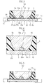
- Figs. 1-4 show a light-emitting diode X1 according to a first embodiment of the present invention.
- the illustrated diode X1 may be used as a backlight for a push button of a small electric device such as a portable telephone.
- the light-emitting diode X1 has a rectangular base unit 1, an LED chip 3A arranged thereon, and a casing 5 enclosing the LED chip 3A.
- the base unit 1 includes a rectangular insulating substrate 1A, a first electrode 2A and a second electrode 2B. Since the substrate 1A is required to have excellent insulating and heat-resistant properties, it may be made of a polyimide resin such as BT resin (trade name, manufactured by MITSUBISHI GAS CHEMICAL CO.,INC.), or a ceramic material.
- each of the electrodes 2A, 2B is formed on the substrate 1A, extending from the upper surface 10 through a side surface 11 to the lower surface 12 of the substrate 1A.
- the electrodes 2A, 2B are spaced from each other to be electrically insulated.
- the electrodes 2A, 2B may be formed in the following manner. First, a conductive metal layer made of e.g. copper or nickel is formed on the substrate 1A, and then etched to remove unnecessary portions. At this stage, two separate conductive elements (one for the first electrode 2A and the other for the second electrode 2B) are formed. Finally, the conductive elements are gold-plated by e.g. electroplating to provide the first and the second electrodes 2A, 2B. As a result of such gold-plating, the electrodes 2A, 2B become highly resistant to oxidation, and a wire will be firmly bonded to these electrodes.
- a conductive metal layer made of e.g. copper or nickel is formed on the substrate 1A, and then etched to remove unnecessary portions. At this stage, two separate conductive elements (one for the first electrode 2A and the other for the second electrode 2B) are formed. Finally, the conductive elements are gold-plated by e.g. electroplating to provide the first and the second electrodes 2A, 2
- the first electrode 2A has an upper portion 2a formed on the upper surface 10 of the substrate 1A.
- the upper portion 2a includes a die-bonding region 20a (protruding toward the second electrode 2B) onto which the LED chip 3A is mounted.
- silver paste is applied between the LED chip 3A and the die-bonding region 20a, so that the chip 3A and the region 20a are electrically and fixedly connected to each other.
- the second electrode 2B has an upper portion 2b formed on the upper surface 10 of the insulating substrate 1A.
- the upper portion 2b includes a wire-bonding region 20b protruding the first electrode 2A.
- the wire-bonding region 20b and the top surface 30 of the LED chip 3A are electrically connected to each other by a wire 4 made of gold for example.
- the casing 5 placed on the base unit 1 is formed with a cavity 50a for housing the LED chip 3A and the wire 4.
- the cavity 50a is defined by an inner wall surface 5a of the casing 5.
- the cavity 50a extends through the thickness of the casing 5 to be open upward and downward.
- the cavity 50a is filled up with a transparent resin material which is highly permeable to light.
- the resin material may be an epoxy resin containing no filler. After being hardened, the transparent resin material serves as a light-permeable member 50.
- the casing 5 is made of a highly reflective white material such as a polycarbonate resin containing a titanium oxide as filler. Accordingly, the inner wall surface 5a of the casing 5 is rendered highly reflective. Thus, the inner wall surface 5a serves as an excellent reflector for light emitted from the LED chip 3A.
- the inner wall surface 5a gives an elliptical appearance, while as viewed in two vertical sections intersecting at right angles (see Figs. 3 and 4), it gives an appearance of a quadric curve (curve of second order).
- the light-permeable member 50 fitted in the cavity 50a, has the same curved surface as the inner wall surface 5a.
- the casing 5 and the light-permeable member 50 are formed as follows.
- the casing 5, which is made of the above-mentioned resin material by e.g. transfer molding, is prepared separately from the light-permeable member 50.
- the casing 5 is then attached to the base unit 1 (onto which the LED chip 3A with the wire 4 has already been mounted).
- a transparent resin is filled into the cavity 50a of the casing 5 by potting, thereby forming the light-permeable member 50.
- the light-permeable member 50 may be formed by transfer molding.
- the light-emitting diode X1 described above has the following advantages.
- the LED chip 3A When voltage is applied to the light-emitting diode X1 in the forward direction, the LED chip 3A emits light. Part of the light emitted from the LED chip 3A passes through the light-permeable member 50 without reflection. On the other hand, the remaining part of the emitted light is reflected (once or more) by the inner wall surface 5a (which is highly reflective) while traveling through the light-permeable member 50. The thus reflected light and non-reflected light are eventually emitted from the light-permeable member 50 to form a light beam together.
- the inner wall surface 5a defines an elliptical figure in the top surface of the casing 5 as shown in Fig. 2, the light beam from the light-emitting diode X1 is also elliptical in horizontal cross-section. Therefore, even if a portable telephone has an elongated push button, a single light-emitting diode X1 suffices for lighting up the entirety of the push button. Thus, there is no need to use a plurality of light-emitting diodes for a single push button.
- the inner wall surface 5a forms a quadric surface (part of a generally elliptic paraboloid), light beams emitted from the diode X1 are advantageously directed toward substitutionally the same direction.
- the inner wall 5a of the casing 5 works as the reflector.
- the present invention is not limited to this arrangement.
- Fig. 5 showing a light-emitting diode X2 according to a second embodiment of the present invention.
- the illustrated diode X2 is basically similar to the diode X1 of the first embodiment, except that use is made of a light-reflecting film 52b as a reflector formed on the inner wall surface 52a of a casing 52.
- the light-reflecting film 52b may be prepared by sputtering or vacuum evaporation of high light-reflective metal.
- the film 52b may be made of a reflective resin material such as polycarbonate resin containing titanium oxide.
- the reflective inner wall surface 5a (the first embodiment) and the additional reflecting film 52b (the second embodiment) both taper toward the LED chip.
- Fig. 6 shows a light-emitting diode X3 according to a third embodiment of the present invention.
- the illustrated diode X3 is basically similar to the diode X1 of the first embodiment, except that the inner wall surface 53a of a casing 53 appears, in horizontal section, to be oblong but not elliptic.
- the second embodiment X2 Fig. 5
- no separate reflective film is formed on the inner wall surface 53a of the casing 53.
- the casing 53 needs to be made of a reflective resin material.
- Fig. 7 shows a light-emitting diode X4 according to a fourth embodiment of the present invention.
- the illustrated diode X4 is basically similar to the diode X1 of the first embodiment, except that the inner wall surface 54a of a casing 54 appears, in horizontal section, to be rhombic.
- Fig. 8 shows a light-emitting diode X5 according to a fifth embodiment of the present invention.
- the illustrated diode X5 is basically similar to the diode X1 of the first embodiment, except that the inner wall surface 55a of a casing 55 appears, in horizontal section, to be rectangular.
- Fig. 9 shows a semiconductor device X6 according to a sixth embodiment of the present invention.
- the illustrated device X6 includes an LD (laser diode) chip 3B instead of an LED chip.
- the LD chip 3B are provided with two terminals 36a and 36b facing in the same direction (downward).
- One terminal 36a is connected, via a conductor 34A, to a first electrode 26A formed on an insulating substrate 16, while the other terminal 36b is connected, via another conductor 34B, to a second electrode 26B.
- a casing 56 may be similar in configuration to the casing 5 of the first embodiment, so that the inner wall surface 56a of this embodiment and the counterpart of the first embodiment may also be similar.
- Fig. 10 shows a laser diode X7 according to a seventh embodiment of the present invention.
- the illustrated diode X7 is basically similar to the diode X6 of the sixth embodiment (Fig. 9) except for the following points.
- First, an LD chip 37B is mounted onto a first electrode 27A only so as not to be in direct contact with a second electrode 27B.
- Second, two terminals 37a and 37b of the LD chip 37B are directed upward.
- use is made of a wire 47a for connecting one terminal 37a to the first electrode 27A, while another wire 47b is used for connecting the other terminal 37b to the second electrode 27B.
- Fig. 11 shows a laser diode X8 according to an eighth embodiment of the present invention.
- the illustrated diode X8 is basically similar to the diode X7 of the seventh embodiment (Fig. 10), except that an LD chip 38B is arranged between first and second electrodes 28A, 28B, so that the chip 38B is mounted directly on an insulating substrate 18.
Landscapes
- Led Device Packages (AREA)
- Push-Button Switches (AREA)
- Led Devices (AREA)
Abstract
Description
Claims (19)
- A semiconductor device (X1-X8) comprising:characterized in that the reflector (5, 52b, 53-56) has an elongated transverse section.a substrate (1A, 16, 18) provided with a first electrode (2A, 26A-28A) and a second electrode (2B, 26B-28B) formed thereon;a semiconductor chip (3A, 3B, 37B, 38B) mounted on the substrate (1A, 16, 18) for emitting light, the semiconductor chip (3A, 3B, 37B, 38B) being electrically connected to the first electrode (2A, 26A-28A) and the second electrode (2B, 26B-28B); anda reflector (5, 52b, 53-56) enclosing the semiconductor chip (3A, 3B, 37B, 38B) for reflecting the light emitted from the semiconductor chip (3A, 3B, 37B, 38B);
- The semiconductor device according to claim 1, wherein the reflector (5, 52b, 53-56) has a first vertical section defining a quadric curve.
- The semiconductor device according to claim 2, wherein the reflector (5, 52b, 53-56) has a second vertical section intersecting the first vertical section at right angles, the second vertical section defining a quadric curve.
- The semiconductor device according to any one of claims 1-3, wherein the reflector (5, 52b, 53-56) defines a quadric surface tapering toward the semiconductor chip (3A, 3B, 37B, 38B).
- The semiconductor device according to any one of claims 1-4, wherein the semiconductor chip is a light-emitting diode chip (3A, 3B).
- The semiconductor device according to any one of claims 1-4, wherein the semiconductor chip is a laser diode chip (37B, 38B).
- The semiconductor device according to any one of claims 1-6, further comprising a casing (5, 52-56) supported by the substrate (1A, 16, 18), the casing (5, 52-56) being provided with an inner surface (5a, 52a-56a) defining a cavity (50a), the inner surface (5a, 52a-56a) serving as the reflector.
- The semiconductor device according to claim 7, wherein the casing (5, 52-56) is made of a reflective material.
- The semiconductor device according to claim 7 or 8, wherein the casing (5, 52-56) is white.
- The semiconductor device according to any one of claims 7-9, wherein the casing (5, 52-56) is made of a polycarbonate resin containing titanium oxide.
- The semiconductor device according to claim 1, further comprising a casing (52) supported by the substrate and a light reflecting film (52b) as the reflector, the casing (52) being provided with an inner surface (52a) defining a cavity, the light reflecting film (52b) being formed on the inner surface (52a).
- The semiconductor device according to claim 11, wherein the light reflecting film (52b) is made of metal.
- The semiconductor device according to claim 11 or 12, wherein the light reflecting film (52b) is white.
- The semiconductor device according to claim 11, wherein the light reflecting film (52b) is made of a polycarbonate resin containing titanium oxide.
- The semiconductor device according to any one of claims 1-14, further comprising a light-permeable member (50), wherein the reflector (5, 52b, 53-56) defines a space accommodating the light-permeable member (50).
- The semiconductor device according to claim 15, wherein the light-permeable member (50) is made of an epoxy resin.
- The semiconductor device according to any one of claims 1-16, wherein the elongated transverse section is elliptical.
- The semiconductor device according to any one of claims 1-16, wherein the elongated transverse section is rhombic.
- The semiconductor device according to any one of claims 1-16, wherein the elongated transverse section is rectangular.
Applications Claiming Priority (2)
| Application Number | Priority Date | Filing Date | Title |
|---|---|---|---|
| JP35707498 | 1998-12-16 | ||
| JP35707498A JP2000183407A (en) | 1998-12-16 | 1998-12-16 | Optical semiconductor device |
Publications (3)
| Publication Number | Publication Date |
|---|---|
| EP1011151A2 true EP1011151A2 (en) | 2000-06-21 |
| EP1011151A3 EP1011151A3 (en) | 2001-08-01 |
| EP1011151B1 EP1011151B1 (en) | 2007-09-19 |
Family
ID=18452258
Family Applications (1)
| Application Number | Title | Priority Date | Filing Date |
|---|---|---|---|
| EP99310103A Expired - Lifetime EP1011151B1 (en) | 1998-12-16 | 1999-12-15 | Semiconductor device with reflector |
Country Status (6)
| Country | Link |
|---|---|
| US (1) | US6355946B1 (en) |
| EP (1) | EP1011151B1 (en) |
| JP (1) | JP2000183407A (en) |
| KR (1) | KR100708034B1 (en) |
| DE (1) | DE69937137T2 (en) |
| TW (1) | TW457520B (en) |
Cited By (14)
| Publication number | Priority date | Publication date | Assignee | Title |
|---|---|---|---|---|
| WO2006032251A1 (en) * | 2004-09-22 | 2006-03-30 | Osram Opto Semiconductors Gmbh | Housing for an optoelectronic component, optoelectronic component and method for the production of an optoelectronic component |
| WO2006082559A1 (en) * | 2005-02-07 | 2006-08-10 | Koninklijke Philips Electronics N.V. | Beam shaper in led package |
| EP1564819A4 (en) * | 2002-11-05 | 2006-10-04 | Matsushita Electric Industrial Co Ltd | OF THE |
| DE10229067B4 (en) * | 2002-06-28 | 2007-08-16 | Osram Opto Semiconductors Gmbh | Optoelectronic component and method for its production |
| WO2009141762A1 (en) | 2008-05-20 | 2009-11-26 | Koninklijke Philips Electronics N.V. | Optical element for asymmetric light distribution |
| WO2010001309A1 (en) * | 2008-07-01 | 2010-01-07 | Koninklijke Philips Electronics N.V. | Close proximity collimator for led |
| US7670038B2 (en) | 2004-09-20 | 2010-03-02 | Koninklijke Philips Electronics N.V. | LED collimator element with an asymmetrical collimator |
| EP1521313A3 (en) * | 2003-10-03 | 2010-12-29 | Philips Lumileds Lighting Company LLC | Integrated reflector cup for a light emitting device mount |
| EP2270889A3 (en) * | 2002-12-06 | 2011-02-02 | Cree, Inc. | LED package comprising leadframe and two-part heatsink |
| CN102549785A (en) * | 2009-10-01 | 2012-07-04 | 日亚化学工业株式会社 | Light emitting device |
| EP1609835B1 (en) * | 2003-02-25 | 2013-01-09 | Kaneka Corporation | Curing composition and method for preparing same, light-shielding paste, light-shielding resin and method for producing same, package for light-emitting diode, and semiconductor device |
| FR2979487A1 (en) * | 2011-08-23 | 2013-03-01 | Syndica Optical Technology Co Ltd | LED case for increasing e.g. specific lighting of light source used in e.g. household appliances, has chip enclosed by enclosure on base, and filling material solidified to form filling lens such that chip is encapsulated in lens |
| EP3297036A1 (en) * | 2009-09-24 | 2018-03-21 | MSG Lithoglas GmbH | Method for producing an assembly comprising a component on a carrier substrate and assembly and method for producing a semi-finished product |
| EP2834295B1 (en) * | 2012-04-05 | 2019-01-09 | SABIC Global Technologies B.V. | High reflectance polycarbonate |
Families Citing this family (111)
| Publication number | Priority date | Publication date | Assignee | Title |
|---|---|---|---|---|
| US6434598B1 (en) * | 1996-07-01 | 2002-08-13 | Sun Microsystems, Inc. | Object-oriented system, method and article of manufacture for a client-server graphical user interface (#9) framework in an interprise computing framework system |
| JP3785820B2 (en) * | 1998-08-03 | 2006-06-14 | 豊田合成株式会社 | Light emitting device |
| JP3503131B2 (en) * | 1999-06-03 | 2004-03-02 | サンケン電気株式会社 | Semiconductor light emitting device |
| JP4125848B2 (en) * | 1999-12-17 | 2008-07-30 | ローム株式会社 | Chip type light emitting device with case |
| JP4926337B2 (en) * | 2000-06-28 | 2012-05-09 | アバゴ・テクノロジーズ・ジェネラル・アイピー(シンガポール)プライベート・リミテッド | light source |
| CN1245586C (en) * | 2000-07-07 | 2006-03-15 | 宇宙设备公司 | a luminous screen |
| JP2002050797A (en) * | 2000-07-31 | 2002-02-15 | Toshiba Corp | Semiconductor-excited phosphor light emitting device and method of manufacturing the same |
| JP2002064224A (en) * | 2000-08-18 | 2002-02-28 | Agilent Technologies Japan Ltd | Light emitting diode and method of manufacturing the same |
| JP3930710B2 (en) * | 2000-09-13 | 2007-06-13 | シチズン電子株式会社 | Chip-type light emitting diode and manufacturing method thereof |
| KR100367182B1 (en) * | 2001-01-04 | 2003-01-09 | 이성재 | LED Lamp |
| JP2002299698A (en) * | 2001-03-30 | 2002-10-11 | Sumitomo Electric Ind Ltd | Light emitting device |
| TW543128B (en) * | 2001-07-12 | 2003-07-21 | Highlink Technology Corp | Surface mounted and flip chip type LED package |
| JP2003051620A (en) * | 2001-08-08 | 2003-02-21 | Rohm Co Ltd | Semiconductor light emitting device |
| US8201985B2 (en) * | 2001-08-24 | 2012-06-19 | Cao Group, Inc. | Light bulb utilizing a replaceable LED light source |
| US7976211B2 (en) * | 2001-08-24 | 2011-07-12 | Densen Cao | Light bulb utilizing a replaceable LED light source |
| US7728345B2 (en) * | 2001-08-24 | 2010-06-01 | Cao Group, Inc. | Semiconductor light source for illuminating a physical space including a 3-dimensional lead frame |
| US8569785B2 (en) * | 2001-08-24 | 2013-10-29 | Cao Group, Inc. | Semiconductor light source for illuminating a physical space including a 3-dimensional lead frame |
| KR20030024283A (en) * | 2001-09-17 | 2003-03-26 | 광전자 주식회사 | A lead frame having radiation of heat, an optical semiconductor device having that, the manufacturing method, and a semiconductor device |
| US6974234B2 (en) * | 2001-12-10 | 2005-12-13 | Galli Robert D | LED lighting assembly |
| USD509196S1 (en) | 2002-05-13 | 2005-09-06 | Nichia Corporation | Light emitting diode |
| USD494938S1 (en) | 2002-05-13 | 2004-08-24 | Nichia Corporation | Light emitting diode |
| US7336403B2 (en) * | 2002-05-27 | 2008-02-26 | Canon Kabushiki Kaisha | Optical element and illumination apparatus having same |
| KR100567550B1 (en) * | 2002-05-29 | 2006-04-05 | 서울반도체 주식회사 | Pink light emitting diode and method of manufacturing the same |
| TW546799B (en) * | 2002-06-26 | 2003-08-11 | Lingsen Precision Ind Ltd | Packaged formation method of LED and product structure |
| KR100567559B1 (en) * | 2002-07-25 | 2006-04-05 | 마츠시다 덴코 가부시키가이샤 | Device with photoelectric element |
| US6730940B1 (en) * | 2002-10-29 | 2004-05-04 | Lumileds Lighting U.S., Llc | Enhanced brightness light emitting device spot emitter |
| JP4185352B2 (en) * | 2002-11-13 | 2008-11-26 | シチズン電子株式会社 | Light emitting diode and manufacturing method thereof |
| USD508233S1 (en) * | 2003-02-26 | 2005-08-09 | Nichia Corporation | Light emitting diode |
| AU2003227020A1 (en) * | 2003-02-27 | 2004-09-17 | Bang And Olufsen A/S | Metal structure with translucent region |
| USD505396S1 (en) * | 2003-03-03 | 2005-05-24 | Nichia Corporation | Light emitting diode |
| JP3977774B2 (en) | 2003-06-03 | 2007-09-19 | ローム株式会社 | Optical semiconductor device |
| JP3878579B2 (en) | 2003-06-11 | 2007-02-07 | ローム株式会社 | Optical semiconductor device |
| USD505398S1 (en) * | 2003-06-24 | 2005-05-24 | Nichia Corporation | Light emitting diode |
| JP2005019541A (en) | 2003-06-24 | 2005-01-20 | Rohm Co Ltd | Optical semiconductor device |
| TWD100417S1 (en) * | 2003-07-09 | 2004-09-21 | 松下電器產業股份有限公司 | Photosensitive integrated circuit components |
| USD505661S1 (en) * | 2003-07-09 | 2005-05-31 | Nichia Corporation | Light emitting diode |
| USD514073S1 (en) * | 2003-07-09 | 2006-01-31 | Nichai Corporation | Light emitting diode |
| TWD100418S1 (en) * | 2003-07-09 | 2004-09-21 | 松下電器產業股份有限公司 | Photosensitive integrated circuit components |
| JP2005056941A (en) * | 2003-08-07 | 2005-03-03 | Citizen Electronics Co Ltd | Light emitting diode |
| US20050201100A1 (en) * | 2003-09-08 | 2005-09-15 | Cassarly William J. | Led lighting assembly |
| USD535263S1 (en) | 2003-09-09 | 2007-01-16 | Nichia Corporation | Light emitting diode |
| USD539760S1 (en) | 2003-09-09 | 2007-04-03 | Nichia Corporation | Light emitting diode |
| USD510913S1 (en) | 2003-09-09 | 2005-10-25 | Nichia Corporation | Light emitting diode |
| USD528515S1 (en) | 2003-09-09 | 2006-09-19 | Nichia Corporation | Light emitting diode |
| USD553103S1 (en) | 2003-09-09 | 2007-10-16 | Nichia Corporation | Light emitting diode |
| US7145182B2 (en) * | 2003-09-12 | 2006-12-05 | Avago Technologies General Ip (Singapore) Pte. Ltd. | Integrated emitter devices having beam divergence reducing encapsulation layer |
| USD505397S1 (en) * | 2003-09-15 | 2005-05-24 | Nichia Corporation | Light emitting diode |
| USD503930S1 (en) * | 2003-09-15 | 2005-04-12 | Nichia Corporation | Light emitting diode |
| USD510912S1 (en) * | 2003-09-15 | 2005-10-25 | Nichia Corporation | Light emitting diode |
| US20080025030A9 (en) * | 2003-09-23 | 2008-01-31 | Lee Kong W | Ceramic packaging for high brightness LED devices |
| US7854535B2 (en) * | 2003-09-23 | 2010-12-21 | Avago Technologies Ecbu Ip (Singapore) Pte. Ltd. | Ceramic packaging for high brightness LED devices |
| JP4773048B2 (en) * | 2003-09-30 | 2011-09-14 | シチズン電子株式会社 | Light emitting diode |
| US7157744B2 (en) * | 2003-10-29 | 2007-01-02 | M/A-Com, Inc. | Surface mount package for a high power light emitting diode |
| USD508235S1 (en) * | 2003-12-05 | 2005-08-09 | Nichia Corporation | Light emitting diode |
| JP2005183531A (en) * | 2003-12-17 | 2005-07-07 | Sharp Corp | Semiconductor light emitting device |
| JP2005197369A (en) | 2004-01-05 | 2005-07-21 | Toshiba Corp | Optical semiconductor device |
| US7696526B2 (en) * | 2004-01-29 | 2010-04-13 | Dominant Opto Tech Sdn Bhd | Surface mount optoelectronic component |
| DE102004014207A1 (en) * | 2004-03-23 | 2005-10-13 | Osram Opto Semiconductors Gmbh | Optoelectronic component with a multi-part housing body |
| DE102004031732A1 (en) * | 2004-06-30 | 2006-01-19 | Osram Opto Semiconductors Gmbh | Radiation-emitting semiconductor chip with a beam-shaping element and beam-shaping element |
| JP2006049807A (en) * | 2004-07-05 | 2006-02-16 | Ngk Spark Plug Co Ltd | Light emitting device package |
| JP4747726B2 (en) * | 2004-09-09 | 2011-08-17 | 豊田合成株式会社 | Light emitting device |
| JP4535928B2 (en) | 2005-04-28 | 2010-09-01 | シャープ株式会社 | Semiconductor light emitting device |
| TWD112798S1 (en) * | 2005-04-28 | 2006-09-01 | 東芝照明技術股份有限公司 | Lighting diode modules |
| KR100719072B1 (en) * | 2005-10-28 | 2007-05-16 | (주) 아모센스 | How to form the slope of the ceramic in the LED package |
| US20070200118A1 (en) * | 2005-12-21 | 2007-08-30 | Epstein Kenneth A | Led light confinement element |
| US7637639B2 (en) * | 2005-12-21 | 2009-12-29 | 3M Innovative Properties Company | LED emitter with radial prismatic light diverter |
| US8044412B2 (en) | 2006-01-20 | 2011-10-25 | Taiwan Semiconductor Manufacturing Company, Ltd | Package for a light emitting element |
| KR101283182B1 (en) * | 2006-01-26 | 2013-07-05 | 엘지이노텍 주식회사 | Package of light-emitting diode and manufacturing method thereof |
| JP4984609B2 (en) * | 2006-04-05 | 2012-07-25 | 日亜化学工業株式会社 | Support for mounting semiconductor element and semiconductor device |
| TWD117963S1 (en) * | 2006-04-05 | 2007-07-01 | 首爾半導體股份有限公司 | Light emitting diode (led) |
| JP2007281260A (en) * | 2006-04-07 | 2007-10-25 | Sumitomo Metal Electronics Devices Inc | Reflector, light emitting element storage package using the reflector, and lens used for the reflector |
| CN101060107A (en) * | 2006-04-19 | 2007-10-24 | 陈劲豪 | Plant base structure of luminescent crystal |
| JP4605789B2 (en) * | 2006-05-29 | 2011-01-05 | 株式会社小糸製作所 | Light emitting module and vehicle lamp |
| US7993038B2 (en) | 2007-03-06 | 2011-08-09 | Toyoda Gosei Co., Ltd. | Light-emitting device |
| KR101318972B1 (en) * | 2007-03-30 | 2013-10-17 | 서울반도체 주식회사 | Light emitting diode and method of manufacturing the same |
| KR100901618B1 (en) | 2007-04-19 | 2009-06-08 | 엘지이노텍 주식회사 | Light emitting diode package and manufacturing method |
| US7967476B2 (en) * | 2007-07-04 | 2011-06-28 | Nichia Corporation | Light emitting device including protective glass film |
| TWI337783B (en) * | 2007-07-06 | 2011-02-21 | Harvatek Corp | Through hole type led chip package structure using ceramic material as a substrate and method of the same |
| US20090016066A1 (en) * | 2007-07-12 | 2009-01-15 | Chen Pi Hsiang | Package Structure for a High-Luminance Light Source |
| US20090032829A1 (en) * | 2007-07-30 | 2009-02-05 | Tong Fatt Chew | LED Light Source with Increased Thermal Conductivity |
| US20090059573A1 (en) * | 2007-08-29 | 2009-03-05 | James Bears | Solid-state lighting device |
| CN103145751B (en) | 2007-11-09 | 2016-06-08 | 株式会社钟化 | The preparation method of cyclic polyorganosiloxane, solidifying agent, solidification compound and cured article thereof |
| KR101488448B1 (en) * | 2007-12-06 | 2015-02-02 | 서울반도체 주식회사 | Led package and method for fabricating the same |
| CN101896537B (en) | 2007-12-10 | 2012-10-24 | 株式会社钟化 | Curable composition having alkali developability, insulating film and thin film transistor using same |
| US20090273940A1 (en) * | 2008-05-01 | 2009-11-05 | Cao Group, Inc. | LED lighting device |
| TWM353308U (en) * | 2008-06-09 | 2009-03-21 | qiu-shuang Ke | LED illumination device |
| KR100999699B1 (en) * | 2008-09-01 | 2010-12-08 | 엘지이노텍 주식회사 | Light emitting device package |
| US9252336B2 (en) * | 2008-09-26 | 2016-02-02 | Bridgelux, Inc. | Multi-cup LED assembly |
| WO2010038767A1 (en) | 2008-10-02 | 2010-04-08 | 株式会社カネカ | Photocurable composition and cured product |
| KR101018191B1 (en) | 2008-11-27 | 2011-02-28 | 삼성엘이디 주식회사 | Ceramic package and headlamp module having same |
| JP4799606B2 (en) | 2008-12-08 | 2011-10-26 | 株式会社東芝 | Optical semiconductor device and method for manufacturing optical semiconductor device |
| KR20110117090A (en) * | 2009-02-17 | 2011-10-26 | 카오 그룹, 인코포레이티드 | LED light bulbs for space lighting |
| US8089075B2 (en) * | 2009-04-17 | 2012-01-03 | Avago Technologies Ecbu Ip (Singapore) Pte. Ltd. | LFCC package with a reflector cup surrounded by a single encapsulant |
| US8101955B2 (en) * | 2009-04-17 | 2012-01-24 | Avago Technologies Ecbu Ip (Singapore) Pte. Ltd. | PLCC package with a reflector cup surrounded by an encapsulant |
| JP4875185B2 (en) | 2010-06-07 | 2012-02-15 | 株式会社東芝 | Optical semiconductor device |
| TW201250964A (en) * | 2011-01-27 | 2012-12-16 | Dainippon Printing Co Ltd | Resin-attached lead frame, method for manufacturing same, and lead frame |
| JP2013016723A (en) * | 2011-07-06 | 2013-01-24 | Panasonic Corp | Photographing illumination device |
| US9290618B2 (en) | 2011-08-05 | 2016-03-22 | Sabic Global Technologies B.V. | Polycarbonate compositions having enhanced optical properties, methods of making and articles comprising the polycarbonate compositions |
| CN103000794B (en) * | 2011-09-14 | 2015-06-10 | 展晶科技(深圳)有限公司 | LED package structure |
| JP2013084690A (en) * | 2011-10-06 | 2013-05-09 | Sharp Corp | Light-emitting diode package and backlight device |
| WO2013130610A1 (en) | 2012-02-29 | 2013-09-06 | Sabic Innovative Plastics Ip B.V. | Polycarbonate compositions containing conversions material chemistry and having enhanced optical properties, methods of making and articles comprising the same |
| US9346949B2 (en) | 2013-02-12 | 2016-05-24 | Sabic Global Technologies B.V. | High reflectance polycarbonate |
| US9090759B2 (en) * | 2012-04-05 | 2015-07-28 | Sabic Global Technologies B.V. | High reflectance polycarbonate |
| WO2014024371A1 (en) * | 2012-08-10 | 2014-02-13 | パナソニック株式会社 | Semiconductor light-emitting device |
| EP2912107B1 (en) | 2012-10-25 | 2018-03-28 | SABIC Global Technologies B.V. | Light emitting diode devices, method of manufacture, uses thereof |
| KR20160038568A (en) * | 2014-09-30 | 2016-04-07 | (주)포인트엔지니어링 | Chip substrate comprising plural curve surface cavity |
| JP6736256B2 (en) * | 2015-03-23 | 2020-08-05 | ローム株式会社 | LED package |
| US11444227B2 (en) | 2019-10-01 | 2022-09-13 | Dominant Opto Technologies Sdn Bhd | Light emitting diode package with substrate configuration having enhanced structural integrity |
| TW202530854A (en) * | 2020-04-17 | 2025-08-01 | 美商恩特葛瑞斯股份有限公司 | Reticle pod having coated sensor zones and method of producing reticle pod |
| US11444225B2 (en) | 2020-09-08 | 2022-09-13 | Dominant Opto Technologies Sdn Bhd | Light emitting diode package having a protective coating |
| US11329206B2 (en) | 2020-09-28 | 2022-05-10 | Dominant Opto Technologies Sdn Bhd | Lead frame and housing sub-assembly for use in a light emitting diode package and method for manufacturing the same |
Family Cites Families (14)
| Publication number | Priority date | Publication date | Assignee | Title |
|---|---|---|---|---|
| US3991339A (en) * | 1975-05-27 | 1976-11-09 | Rca Corporation | Light emitting diode with reflector |
| US4013916A (en) * | 1975-10-03 | 1977-03-22 | Monsanto Company | Segmented light emitting diode deflector segment |
| FR2378325A1 (en) * | 1977-01-20 | 1978-08-18 | Radiotechnique Compelec | ELECTROLUMINESCENT DISPLAY ELEMENT |
| US4152624A (en) * | 1978-03-16 | 1979-05-01 | Monsanto Company | Molded LED indicator |
| JPS60262476A (en) | 1984-06-08 | 1985-12-25 | Matsushita Electric Ind Co Ltd | Light-emitting element |
| US4914731A (en) * | 1987-08-12 | 1990-04-03 | Chen Shen Yuan | Quickly formed light emitting diode display and a method for forming the same |
| US4964025A (en) * | 1988-10-05 | 1990-10-16 | Hewlett-Packard Company | Nonimaging light source |
| US5291038A (en) * | 1990-12-19 | 1994-03-01 | Sharp Kabushiki Kaisha | Reflective type photointerrupter |
| US5479426A (en) * | 1994-03-04 | 1995-12-26 | Matsushita Electronics Corporation | Semiconductor laser device with integrated reflector on a (511) tilted lattice plane silicon substrate |
| DE4446566A1 (en) | 1994-12-24 | 1996-06-27 | Telefunken Microelectron | Multipole, surface-mountable, electronic component |
| JPH08204239A (en) | 1995-01-31 | 1996-08-09 | Rohm Co Ltd | Resin-sealed light emitting device |
| DE19549818B4 (en) | 1995-09-29 | 2010-03-18 | Osram Opto Semiconductors Gmbh | Optoelectronic semiconductor device |
| US6274890B1 (en) * | 1997-01-15 | 2001-08-14 | Kabushiki Kaisha Toshiba | Semiconductor light emitting device and its manufacturing method |
| JPH10161570A (en) * | 1997-12-12 | 1998-06-19 | Rohm Co Ltd | LED numeric display |
-
1998
- 1998-12-16 JP JP35707498A patent/JP2000183407A/en active Pending
-
1999
- 1999-12-09 KR KR1019990056036A patent/KR100708034B1/en not_active Expired - Fee Related
- 1999-12-09 TW TW088121534A patent/TW457520B/en active
- 1999-12-15 DE DE69937137T patent/DE69937137T2/en not_active Expired - Lifetime
- 1999-12-15 EP EP99310103A patent/EP1011151B1/en not_active Expired - Lifetime
- 1999-12-15 US US09/464,515 patent/US6355946B1/en not_active Expired - Lifetime
Cited By (24)
| Publication number | Priority date | Publication date | Assignee | Title |
|---|---|---|---|---|
| US7795633B2 (en) | 2002-06-28 | 2010-09-14 | Osram Opto Semiconductors Gmbh | Optoelectronic component |
| US8314441B2 (en) | 2002-06-28 | 2012-11-20 | Osram Opto Semiconductors Gmbh | Optoelectronic component |
| DE10229067B4 (en) * | 2002-06-28 | 2007-08-16 | Osram Opto Semiconductors Gmbh | Optoelectronic component and method for its production |
| US7429758B2 (en) | 2002-06-28 | 2008-09-30 | Osram Opto Semiconductor Gmbh | Optoelectronic component and method for producing it |
| US7514279B2 (en) | 2002-06-28 | 2009-04-07 | Osram Opto Semiconductors Gmbh | Optoelectronic component and method for producing it |
| US7948046B2 (en) | 2002-06-28 | 2011-05-24 | Osram Opto Semiconductor Gmbh | Optoelectronic component |
| EP1564819A4 (en) * | 2002-11-05 | 2006-10-04 | Matsushita Electric Industrial Co Ltd | OF THE |
| US7347603B2 (en) | 2002-11-05 | 2008-03-25 | Matsushita Electric Industrial Co., Ltd. | Light-emitting diode |
| EP2270889A3 (en) * | 2002-12-06 | 2011-02-02 | Cree, Inc. | LED package comprising leadframe and two-part heatsink |
| EP1609835B1 (en) * | 2003-02-25 | 2013-01-09 | Kaneka Corporation | Curing composition and method for preparing same, light-shielding paste, light-shielding resin and method for producing same, package for light-emitting diode, and semiconductor device |
| EP1521313A3 (en) * | 2003-10-03 | 2010-12-29 | Philips Lumileds Lighting Company LLC | Integrated reflector cup for a light emitting device mount |
| US7670038B2 (en) | 2004-09-20 | 2010-03-02 | Koninklijke Philips Electronics N.V. | LED collimator element with an asymmetrical collimator |
| US8227821B2 (en) | 2004-09-22 | 2012-07-24 | Osram Opto Semiconductors Gmbh | Housing for an optoelectronic component, optoelectronic component and method for the production of an optoelectronic component |
| WO2006032251A1 (en) * | 2004-09-22 | 2006-03-30 | Osram Opto Semiconductors Gmbh | Housing for an optoelectronic component, optoelectronic component and method for the production of an optoelectronic component |
| WO2006082559A1 (en) * | 2005-02-07 | 2006-08-10 | Koninklijke Philips Electronics N.V. | Beam shaper in led package |
| WO2009141762A1 (en) | 2008-05-20 | 2009-11-26 | Koninklijke Philips Electronics N.V. | Optical element for asymmetric light distribution |
| CN102037276B (en) * | 2008-05-20 | 2014-04-16 | 皇家飞利浦电子股份有限公司 | Optical element for asymmetric light distribution |
| RU2523779C2 (en) * | 2008-05-20 | 2014-07-20 | Конинклейке Филипс Электроникс Н.В. | Optical element for asymmetric light distribution |
| WO2010001309A1 (en) * | 2008-07-01 | 2010-01-07 | Koninklijke Philips Electronics N.V. | Close proximity collimator for led |
| EP3297036A1 (en) * | 2009-09-24 | 2018-03-21 | MSG Lithoglas GmbH | Method for producing an assembly comprising a component on a carrier substrate and assembly and method for producing a semi-finished product |
| CN102549785A (en) * | 2009-10-01 | 2012-07-04 | 日亚化学工业株式会社 | Light emitting device |
| CN102549785B (en) * | 2009-10-01 | 2014-12-17 | 日亚化学工业株式会社 | Light emitting device |
| FR2979487A1 (en) * | 2011-08-23 | 2013-03-01 | Syndica Optical Technology Co Ltd | LED case for increasing e.g. specific lighting of light source used in e.g. household appliances, has chip enclosed by enclosure on base, and filling material solidified to form filling lens such that chip is encapsulated in lens |
| EP2834295B1 (en) * | 2012-04-05 | 2019-01-09 | SABIC Global Technologies B.V. | High reflectance polycarbonate |
Also Published As
| Publication number | Publication date |
|---|---|
| EP1011151B1 (en) | 2007-09-19 |
| TW457520B (en) | 2001-10-01 |
| EP1011151A3 (en) | 2001-08-01 |
| JP2000183407A (en) | 2000-06-30 |
| US6355946B1 (en) | 2002-03-12 |
| DE69937137T2 (en) | 2008-01-10 |
| DE69937137D1 (en) | 2007-10-31 |
| KR20000048017A (en) | 2000-07-25 |
| KR100708034B1 (en) | 2007-04-16 |
Similar Documents
| Publication | Publication Date | Title |
|---|---|---|
| US6355946B1 (en) | Semiconductor device with reflector | |
| JP4174823B2 (en) | Semiconductor light emitting device | |
| US7070304B2 (en) | Light emitting diode | |
| US8476656B2 (en) | Light-emitting diode | |
| JP4082544B2 (en) | Back-mounted chip light-emitting device | |
| JP2000223752A (en) | Optical semiconductor device and its forming method | |
| JPH11163419A (en) | Light emitting device | |
| JP2001144333A (en) | Light-emitting device and manufacturing method therefor | |
| JP2011233800A (en) | Light emission element module | |
| KR100851183B1 (en) | Semiconductor light emitting device package | |
| JP2002076443A (en) | Reflective cup for LED chip | |
| US8253159B2 (en) | Semiconductor light emitting device and semiconductor light emitting unit | |
| JP2001308388A (en) | Chip type light emitting device | |
| JP4129169B2 (en) | Light emitting element storage package and light emitting device | |
| KR101202266B1 (en) | Chip type LED | |
| JP2002368278A (en) | Light emitting diode | |
| US11417812B2 (en) | Semiconductor light emitting device | |
| JP2003008078A (en) | Surface mount type semiconductor light emitting device | |
| JP3256951B2 (en) | Light emitting diode | |
| US7307288B2 (en) | Semiconductor device and manufacturing method thereof | |
| JP4129173B2 (en) | Light emitting element storage package and light emitting device | |
| JP2001358367A (en) | Chip type light emitting device | |
| JP2007208292A (en) | Light emitting device | |
| JP2535786Y2 (en) | Light emitting display | |
| JP2004288657A (en) | Light emitting element storage package and light emitting device |
Legal Events
| Date | Code | Title | Description |
|---|---|---|---|
| PUAI | Public reference made under article 153(3) epc to a published international application that has entered the european phase |
Free format text: ORIGINAL CODE: 0009012 |
|
| AK | Designated contracting states |
Kind code of ref document: A2 Designated state(s): DE FR GB |
|
| AX | Request for extension of the european patent |
Free format text: AL;LT;LV;MK;RO;SI |
|
| PUAL | Search report despatched |
Free format text: ORIGINAL CODE: 0009013 |
|
| AK | Designated contracting states |
Kind code of ref document: A3 Designated state(s): AT BE CH CY DE DK ES FI FR GB GR IE IT LI LU MC NL PT SE |
|
| AX | Request for extension of the european patent |
Free format text: AL;LT;LV;MK;RO;SI |
|
| 17P | Request for examination filed |
Effective date: 20020125 |
|
| AKX | Designation fees paid |
Free format text: DE FR GB |
|
| GRAP | Despatch of communication of intention to grant a patent |
Free format text: ORIGINAL CODE: EPIDOSNIGR1 |
|
| GRAS | Grant fee paid |
Free format text: ORIGINAL CODE: EPIDOSNIGR3 |
|
| GRAA | (expected) grant |
Free format text: ORIGINAL CODE: 0009210 |
|
| AK | Designated contracting states |
Kind code of ref document: B1 Designated state(s): DE FR GB |
|
| REG | Reference to a national code |
Ref country code: GB Ref legal event code: FG4D |
|
| REF | Corresponds to: |
Ref document number: 69937137 Country of ref document: DE Date of ref document: 20071031 Kind code of ref document: P |
|
| ET | Fr: translation filed | ||
| PLBE | No opposition filed within time limit |
Free format text: ORIGINAL CODE: 0009261 |
|
| STAA | Information on the status of an ep patent application or granted ep patent |
Free format text: STATUS: NO OPPOSITION FILED WITHIN TIME LIMIT |
|
| 26N | No opposition filed |
Effective date: 20080620 |
|
| PGFP | Annual fee paid to national office [announced via postgrant information from national office to epo] |
Ref country code: FR Payment date: 20081212 Year of fee payment: 10 |
|
| PGFP | Annual fee paid to national office [announced via postgrant information from national office to epo] |
Ref country code: GB Payment date: 20081210 Year of fee payment: 10 |
|
| PGFP | Annual fee paid to national office [announced via postgrant information from national office to epo] |
Ref country code: DE Payment date: 20091222 Year of fee payment: 11 |
|
| GBPC | Gb: european patent ceased through non-payment of renewal fee |
Effective date: 20091215 |
|
| REG | Reference to a national code |
Ref country code: FR Ref legal event code: ST Effective date: 20100831 |
|
| PG25 | Lapsed in a contracting state [announced via postgrant information from national office to epo] |
Ref country code: FR Free format text: LAPSE BECAUSE OF NON-PAYMENT OF DUE FEES Effective date: 20091231 |
|
| PG25 | Lapsed in a contracting state [announced via postgrant information from national office to epo] |
Ref country code: GB Free format text: LAPSE BECAUSE OF NON-PAYMENT OF DUE FEES Effective date: 20091215 |
|
| REG | Reference to a national code |
Ref country code: DE Ref legal event code: R119 Ref document number: 69937137 Country of ref document: DE Effective date: 20110701 |
|
| PG25 | Lapsed in a contracting state [announced via postgrant information from national office to epo] |
Ref country code: DE Free format text: LAPSE BECAUSE OF NON-PAYMENT OF DUE FEES Effective date: 20110701 |