EP0996147A1 - Procédé de fabrication de puces semi-conductrice par oxydation anodique - Google Patents
Procédé de fabrication de puces semi-conductrice par oxydation anodique Download PDFInfo
- Publication number
- EP0996147A1 EP0996147A1 EP99120334A EP99120334A EP0996147A1 EP 0996147 A1 EP0996147 A1 EP 0996147A1 EP 99120334 A EP99120334 A EP 99120334A EP 99120334 A EP99120334 A EP 99120334A EP 0996147 A1 EP0996147 A1 EP 0996147A1
- Authority
- EP
- European Patent Office
- Prior art keywords
- wafer
- semiconductor chip
- side walls
- semiconductor chips
- semiconductor
- Prior art date
- Legal status (The legal status is an assumption and is not a legal conclusion. Google has not performed a legal analysis and makes no representation as to the accuracy of the status listed.)
- Withdrawn
Links
Images
Classifications
-
- H—ELECTRICITY
- H01—ELECTRIC ELEMENTS
- H01L—SEMICONDUCTOR DEVICES NOT COVERED BY CLASS H10
- H01L21/00—Processes or apparatus adapted for the manufacture or treatment of semiconductor or solid state devices or of parts thereof
- H01L21/02—Manufacture or treatment of semiconductor devices or of parts thereof
- H01L21/02104—Forming layers
- H01L21/02107—Forming insulating materials on a substrate
- H01L21/02225—Forming insulating materials on a substrate characterised by the process for the formation of the insulating layer
- H01L21/02227—Forming insulating materials on a substrate characterised by the process for the formation of the insulating layer formation by a process other than a deposition process
- H01L21/0223—Forming insulating materials on a substrate characterised by the process for the formation of the insulating layer formation by a process other than a deposition process formation by oxidation, e.g. oxidation of the substrate
- H01L21/02233—Forming insulating materials on a substrate characterised by the process for the formation of the insulating layer formation by a process other than a deposition process formation by oxidation, e.g. oxidation of the substrate of the semiconductor substrate or a semiconductor layer
- H01L21/02236—Forming insulating materials on a substrate characterised by the process for the formation of the insulating layer formation by a process other than a deposition process formation by oxidation, e.g. oxidation of the substrate of the semiconductor substrate or a semiconductor layer group IV semiconductor
- H01L21/02238—Forming insulating materials on a substrate characterised by the process for the formation of the insulating layer formation by a process other than a deposition process formation by oxidation, e.g. oxidation of the substrate of the semiconductor substrate or a semiconductor layer group IV semiconductor silicon in uncombined form, i.e. pure silicon
-
- H—ELECTRICITY
- H01—ELECTRIC ELEMENTS
- H01L—SEMICONDUCTOR DEVICES NOT COVERED BY CLASS H10
- H01L21/00—Processes or apparatus adapted for the manufacture or treatment of semiconductor or solid state devices or of parts thereof
- H01L21/02—Manufacture or treatment of semiconductor devices or of parts thereof
- H01L21/02104—Forming layers
- H01L21/02107—Forming insulating materials on a substrate
- H01L21/02225—Forming insulating materials on a substrate characterised by the process for the formation of the insulating layer
- H01L21/02227—Forming insulating materials on a substrate characterised by the process for the formation of the insulating layer formation by a process other than a deposition process
- H01L21/02258—Forming insulating materials on a substrate characterised by the process for the formation of the insulating layer formation by a process other than a deposition process formation by anodic treatment, e.g. anodic oxidation
-
- H—ELECTRICITY
- H01—ELECTRIC ELEMENTS
- H01L—SEMICONDUCTOR DEVICES NOT COVERED BY CLASS H10
- H01L21/00—Processes or apparatus adapted for the manufacture or treatment of semiconductor or solid state devices or of parts thereof
- H01L21/70—Manufacture or treatment of devices consisting of a plurality of solid state components formed in or on a common substrate or of parts thereof; Manufacture of integrated circuit devices or of parts thereof
- H01L21/77—Manufacture or treatment of devices consisting of a plurality of solid state components or integrated circuits formed in, or on, a common substrate
- H01L21/78—Manufacture or treatment of devices consisting of a plurality of solid state components or integrated circuits formed in, or on, a common substrate with subsequent division of the substrate into plural individual devices
Definitions
- the invention relates to a method for producing a Semiconductor chips.
- each for the function of the individual Semiconductor chips are required.
- the structures are made with of the structuring methods known in semiconductor technology, for example by applying a photomask and then Wet or dry etching of the wafer and / or by vapor deposition of the Wafers. After completion of the structures, the individual Semiconductor chips by dividing the wafer from the wafer composite separated and isolated.
- the wafer is first coated with that for the Function of the individual semiconductor chips required structures and then into the flat surface of the wafer channel-like depressions introduced, which the individual Limit semiconductor chips in each case. Then the gutter-like The surface of the wafer has depressions thermoplastic, electrically insulating plastic compound applied and smoothed with a squeegee. The fills up Plastic mass completely from the wells. After curing The plastic mass is used to separate and separate the wafer the semiconductor chips from the wafer composite in the area of the depressions divided. The semiconductor chips then have on their side faces an electrically insulating plastic layer in some areas, which can cover, for example, pn junctions located there.
- thermoplastic Plastic mass when applied to the wafer and when stripping with the squeegee not only with the recesses but also with the flat-sided the structure required for the function of the semiconductor chip surface of the semiconductor chips comes into contact, causing a chemical and / or physical change the structure can come. If the incomplete removal of the thermoplastic material from outside the Well-located surface areas of the semiconductor chip the subsequent assembly of the semiconductor chip on a Carrier, for example by bonding, soldering or gluing essential difficult.
- a wafer is used a mesa structure for one designed as a photodiode Semiconductor chip applied.
- the wafer is first used with a provided photosensitive layer and then in Boundary area of the semiconductor chip whose side walls exposed by digging mesa trenches. After that is the surface of the wafer by anodic oxidation with a Insulation layer provided. On this become a metallic Layer, a layer of a dielectric material as well electrical contacts applied.
- the disadvantage of the process that to connect the contacts with the photosensitive Layer in the anodized layer and the dielectric Layer an opening must be made, for which an additional Masking and etching step is required.
- a method for producing one is already known Semiconductor chips, in which before the wafer is structured with the structures required for the function of the semiconductor chips in the flat surface of the wafer is initially channel-like Wells are made and the surface of the wafer then by a temperature treatment in an oxygen-containing Atmosphere with an electrically insulating semiconductor oxide layer is provided. This will then be outside the channel-like depressions after applying a paint mask Etching removed. Then the for the function of the Semiconductor chips required structures generated.
- This method has the disadvantage, however, that the wafer in the manufacture of the for structures required due to the function of the semiconductor chips of the existing wells then only a comparative one has low mechanical stability.
- DE 43 05 296 C2 also describes a method for producing Semiconductor chips known in mesa technology, in which on a wafer first of all those required for the function of the semiconductor chips Structures are created. Then be in the boundary area the semiconductor chips whose side walls by introducing areas of mesa trenches exposed in the wafer. Subsequently is applied to the flat surface of the wafer by CVD oxidation applied a silicon dioxide layer. After that, they are with their backs of the structure facing away adhering to a carrier film Semiconductor chips through saw cuts along the valley bottoms of the Mesa trenches separated from the wafer. The carrier film is not severed.
- the wafer is therefore initially with those required for the electrical function of the semiconductor chip Structure provided, for example, a surface active sensor, a transistor, an electrode and / or an interdigital capacitor. After that are arranged transversely to the plane of extent of the semiconductor chip Side walls of the semiconductor chip at least in regions exposed.
- a surface active sensor for example, a transistor, an electrode and / or an interdigital capacitor.
- Side walls of the semiconductor chip at least in regions exposed.
- the semiconductor chip is coated with side walls with an electrolyte Connected, for example with sulfuric acid, oxalic acid or potassium permanganate dissolved in water. It is between the Electrolyte and the exposed on the side walls, electrical conductive semiconductor substrate applied an anodizing voltage.
- the wafer or the one made of it manufactured semiconductor chip both before and after application the electrical insulation layer is easy to process. Since the anodic oxidation of the wafer only on the electrically conductive Side of the wafer, the process is self-aligning, i.e. the coating is only carried out where it is required is. For semiconductor chips that have an electrically surface active Having structure (e.g. sensors) the side walls of the semiconductor chip with the electrical Isolation layer an impairment of the surface active Structure or its function avoided. Because the anodic oxidation can also be carried out at room temperature Damage to the electrically active semiconductor structures Heat treatment.
- a mechanically applied one Insulation layer shows the one produced by anodic oxidation Insulation layer also better moisture resistance on because the insulation layer is made by chemical conversion the semiconductor material itself is made and therefore special is well connected with this.
- the method according to the invention is also easy to carry out.
- An embodiment of the invention provides that the side walls the semiconductor chip by introducing a groove-like depression that is exposed in a flat surface of the wafer the wafer is then anodized on the side walls and that the wafer is then used to separate the semiconductor chip from the Wafers along the trough-like surrounding the semiconductor chip Deepening is divided.
- the wafer semiconductor chips located in the recesses Surface of the wafer is introduced and only then is the wafer associated with the electrolyte, for example by the electrolyte is deposited on the wafer surface.
- the Insulating layers on the individual, the semiconductor chips each delimiting depressions each have the same Layer thickness.
- the wafer composite remains during the anodizing the side walls of the semiconductor chip receive.
- the wafer material is preferably through Saws removed. This can make applying a mask and a cumbersome etching of the channel-like depressions is no longer necessary.
- the wafer becomes exposed and anodized simultaneously the side walls of the semiconductor chip during the exposure of the Sidewalls associated with an electrolyte. This can then also be used as a coolant for a mechanical removal tool, such as a saw blade.
- the structure required for the function of the semiconductor chip electrically isolated and / or with one against the electrolyte chemically resistant layer is provided.
- the surface of the structure can, for example, in the usual Way a silicon dioxide layer applied to the semiconductor chip become.
- the semiconductor chip can be produced after the insulation layer into a receptacle of a shape adapted to the semiconductor chip preferably optically transparent carrier plate used be, the semiconductor chip having at least one as Surface-active sensor trained structure flat surface in the surface plane one to the Recording adjacent flat surface of the carrier plate is arranged.
- a semiconductor chip can, for example can be used as a microscopic biosensor by using the in one plane with the surface plane of the carrier plate arranged flat-side surface of the semiconductor chip biological cells are adherently attached in a nutrient medium. The cells can then be observed optically through a microscope be and at the same time by means of on the semiconductor chip existing structures measurements on the cells and / or the Culture medium are carried out.
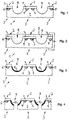
- a wafer 1 is provided with a multiplicity of structures 2, each for the electrical and / or optical function of the individual semiconductor chips 3 are required.
- the Structures 2 using known semiconductor technology methods produced, for example by means of mask technology, by sputtering and / or oxidizing the surface of the wafer 1.
- the structure 2 comprises the individual Semiconductor chips 3 each have an ion-selective field effect transistor, that into the silicon substrate 4 of the wafer 1 diffused drain and source zones 5, 6 with the substrate 4 opposite line type.
- Silicon dioxide layer 7 which the flat surface of the Forms wafers 1 and galvanically isolates them from the substrate 4.
- the outside facing away from the drain and source zones 5, 6 Surface of the silicon dioxide layer 7 forms an electrical active sensor layer, by means of which the field effect transistor Influence is controllable. So can the electrical conductivity between the drain zone 5 and the source zone 6, for example on the surface of silicon dioxide layer 7, in one Fluid contained ions are affected.
- Electrolyte 9 can, for example, sulfuric acid, oxalic acid or in Potassium permanganate dissolved in water can be used.
- an anodizing voltage is applied to the substrate 4 of the wafer 1, which can be, for example, a few volts.
- the insulation layer 10 is formed only on the side walls the semiconductor chips 3, since the electrically conductive semiconductor substrate 4 only comes into contact with the electrolyte 9 there.
- the semiconductor chips 3 can be separated, for example, by a Saw cuts were made in the groove-like recess 8, the width of this saw cut is smaller than the width of the Saw cut, with which the recess 8 in the semiconductor substrate 4 was introduced (Fig. 4).
- a Saw cuts were made in the groove-like recess 8
- the width of this saw cut is smaller than the width of the Saw cut, with which the recess 8 in the semiconductor substrate 4 was introduced (Fig. 4).
- an electrical insulating layer for example a plastic layer become.
- the electrical closes Insulation layer 10 is flush with that on the flat surface of the semiconductor chips 3 located silicon dioxide layer 7. The electrical insulation layer 10 will therefore survive via the electrically active, flat-sided surface of the semiconductor chips 3 avoided.
- the separation of the semiconductor chips 3 and the isolation of the side walls of the semiconductor chips 3 are carried out in one work step by means of anodic oxidation.
- an electrolyte 9 is deposited by saw cuts on the surface of the wafer 1 while exposing the side walls of the semiconductor chips 3.
- An anodizing voltage of a few volts is applied between the electrolyte 9 and the substrate 4 of the wafer 1. While the side walls of the semiconductor chips 3 are exposed, the electrolyte 9 oxidizes the substrate 4 which is already exposed on the side wall regions.
- the electrolyte 9 simultaneously cools the sawing tool 11. In FIG on another, already exposed side wall, an electrical insulation layer 10 is already formed.
Landscapes
- Engineering & Computer Science (AREA)
- Physics & Mathematics (AREA)
- Condensed Matter Physics & Semiconductors (AREA)
- General Physics & Mathematics (AREA)
- Manufacturing & Machinery (AREA)
- Computer Hardware Design (AREA)
- Microelectronics & Electronic Packaging (AREA)
- Power Engineering (AREA)
- Pressure Sensors (AREA)
- Formation Of Insulating Films (AREA)
- Dicing (AREA)
- Weting (AREA)
Applications Claiming Priority (2)
| Application Number | Priority Date | Filing Date | Title |
|---|---|---|---|
| DE19848460 | 1998-10-21 | ||
| DE19848460A DE19848460A1 (de) | 1998-10-21 | 1998-10-21 | Halbleiterbauelement und Verfahren zum Herstellen eines Halbleiterchips |
Publications (1)
| Publication Number | Publication Date |
|---|---|
| EP0996147A1 true EP0996147A1 (fr) | 2000-04-26 |
Family
ID=7885142
Family Applications (1)
| Application Number | Title | Priority Date | Filing Date |
|---|---|---|---|
| EP99120334A Withdrawn EP0996147A1 (fr) | 1998-10-21 | 1999-10-12 | Procédé de fabrication de puces semi-conductrice par oxydation anodique |
Country Status (3)
| Country | Link |
|---|---|
| EP (1) | EP0996147A1 (fr) |
| JP (1) | JP2000133650A (fr) |
| DE (1) | DE19848460A1 (fr) |
Cited By (3)
| Publication number | Priority date | Publication date | Assignee | Title |
|---|---|---|---|---|
| DE10138981A1 (de) * | 2001-08-08 | 2003-03-06 | Infineon Technologies Ag | Verfahren zur elektrochemischen Oxidation eines Halbleiter-Substrats |
| DE10216614A1 (de) * | 2002-04-15 | 2003-10-30 | Infineon Technologies Ag | Verstärkung einer dielektrischen Schicht an Fehlstellen durch selbstjustierende und selbstlimitierende elektrochemische Umwandlung eines Substratmaterials |
| WO2020254499A1 (fr) * | 2019-06-21 | 2020-12-24 | Infineon Technologies Austria Ag | Procédé de fabrication de puces semi-conductrices ayant une étanchéité de paroi latérale |
Families Citing this family (3)
| Publication number | Priority date | Publication date | Assignee | Title |
|---|---|---|---|---|
| JP4927343B2 (ja) * | 2005-03-18 | 2012-05-09 | ルネサスエレクトロニクス株式会社 | 半導体チップおよびその製造方法 |
| JP2009252998A (ja) * | 2008-04-07 | 2009-10-29 | Sanyo Electric Co Ltd | 半導体発光素子およびその製造方法 |
| JP6387244B2 (ja) * | 2014-05-13 | 2018-09-05 | 株式会社ディスコ | ウェーハの加工方法 |
Citations (2)
| Publication number | Priority date | Publication date | Assignee | Title |
|---|---|---|---|---|
| DE4305296A1 (de) * | 1993-02-20 | 1994-08-25 | Telefunken Microelectron | Strahlungsemittierende Diode mit verbesserter Strahlungsleistung |
| US5559058A (en) * | 1994-11-15 | 1996-09-24 | Peter S. Zory, Jr. | Method for producing native oxides on compound semiconductors |
Family Cites Families (2)
| Publication number | Priority date | Publication date | Assignee | Title |
|---|---|---|---|---|
| FR2557371B1 (fr) * | 1983-12-27 | 1987-01-16 | Thomson Csf | Dispositif photosensible comportant entre les detecteurs des zones opaques au rayonnement a detecter, et procede de fabrication |
| JPH0740609B2 (ja) * | 1985-12-20 | 1995-05-01 | セイコー電子工業株式会社 | 半導体装置の製造方法 |
-
1998
- 1998-10-21 DE DE19848460A patent/DE19848460A1/de not_active Withdrawn
-
1999
- 1999-10-12 EP EP99120334A patent/EP0996147A1/fr not_active Withdrawn
- 1999-10-19 JP JP11296919A patent/JP2000133650A/ja active Pending
Patent Citations (2)
| Publication number | Priority date | Publication date | Assignee | Title |
|---|---|---|---|---|
| DE4305296A1 (de) * | 1993-02-20 | 1994-08-25 | Telefunken Microelectron | Strahlungsemittierende Diode mit verbesserter Strahlungsleistung |
| US5559058A (en) * | 1994-11-15 | 1996-09-24 | Peter S. Zory, Jr. | Method for producing native oxides on compound semiconductors |
Non-Patent Citations (1)
| Title |
|---|
| "Semiconductor Chip Insulation by Anodic Oxidation", IBM TECHNICAL DISCLOSURE BULLETIN, vol. 7, no. 6, November 1964 (1964-11-01), US, pages 528 - 529, XP002125071 * |
Cited By (7)
| Publication number | Priority date | Publication date | Assignee | Title |
|---|---|---|---|---|
| DE10138981A1 (de) * | 2001-08-08 | 2003-03-06 | Infineon Technologies Ag | Verfahren zur elektrochemischen Oxidation eines Halbleiter-Substrats |
| US6559069B2 (en) | 2001-08-08 | 2003-05-06 | Infineon Technologies Ag | Process for the electrochemical oxidation of a semiconductor substrate |
| DE10138981B4 (de) * | 2001-08-08 | 2005-09-08 | Infineon Technologies Ag | Verfahren zur Bildung von Siliziumoxid durch elektrochemische Oxidation eines Halbleiter-Substrats mit Vertiefungen |
| DE10216614A1 (de) * | 2002-04-15 | 2003-10-30 | Infineon Technologies Ag | Verstärkung einer dielektrischen Schicht an Fehlstellen durch selbstjustierende und selbstlimitierende elektrochemische Umwandlung eines Substratmaterials |
| DE10216614B4 (de) * | 2002-04-15 | 2004-06-17 | Infineon Technologies Ag | Verfahren zur Verstärkung einer dielektrischen Schicht auf einem Halbleitersubstrat an Fehlstellen und Anordnung mit einer verstärkten dielektrischen Schicht |
| US7176514B2 (en) | 2002-04-15 | 2007-02-13 | Infineon Technologies Ag | Method and configuration for reinforcement of a dielectric layer at defects by self-aligning and self-limiting electrochemical conversion of a substrate material |
| WO2020254499A1 (fr) * | 2019-06-21 | 2020-12-24 | Infineon Technologies Austria Ag | Procédé de fabrication de puces semi-conductrices ayant une étanchéité de paroi latérale |
Also Published As
| Publication number | Publication date |
|---|---|
| JP2000133650A (ja) | 2000-05-12 |
| DE19848460A1 (de) | 2000-05-04 |
Similar Documents
| Publication | Publication Date | Title |
|---|---|---|
| DE3021206C2 (de) | Verfahren zur Herstellung von Leiterbahnen auf Halbleiterbauelementen | |
| DE69836451T2 (de) | Mikroelektronische Struktur von einem schwierig zu ätzenden Material und metallisierte Löcher | |
| DE1930669C2 (de) | Verfahren zur Herstellung einer integrierten Halbleiterschaltung | |
| DE4130555C2 (de) | Halbleitervorrichtung mit hoher Durchbruchsspannung und geringem Widerstand, sowie Herstellungsverfahren | |
| DE2901697B2 (de) | Verfahren zur Ausbildung von Verbindungsleitungen auf einem Substrat | |
| DE69401243T2 (de) | Feldemissionsvorrichtung mit Kleinradiuskathode und Herstellungsverfahren dieser Vorrichtung | |
| DE1803024A1 (de) | Integriertes Halbleiterbauelement und Verfahren zu seiner Herstellung | |
| DE2736200A1 (de) | Chemisch sensitiver feldeffekt- transistor und verfahren zur herstellung desselben | |
| DE2620998A1 (de) | Verfahren zur herstellung von traegern fuer die verarbeitung von ic-chips | |
| DE19832552B4 (de) | Halbleitereinrichtung mit Hohlraum zwischen der Gate-Elektrode und dem Halbleitersubstrat sowie zwischen den Isolationsseitenwandstücken und dem Halbleitersubstrat und Verfahren zu ihrer Herstellung | |
| DE69032074T2 (de) | Verfahren zur Herstellung eines Halbleiterbauteils | |
| EP0996147A1 (fr) | Procédé de fabrication de puces semi-conductrice par oxydation anodique | |
| DE1231812B (de) | Verfahren zur Herstellung von elektrischen Halbleiterbauelementen nach der Mesa-Diffusionstechnik | |
| DE102017200952B4 (de) | Halbleitervorrichtung und Verfahren zur Herstellung einer Halbleitervorrichtung | |
| DE3145101C2 (de) | Verfahren zur Herstellung eines Halbleiterspeichers | |
| DE4310205C1 (de) | Verfahren zur Herstellung einer Lochstruktur in einem Substrat aus Silizium | |
| DE10350036A1 (de) | Verfahren zum Vereinzeln von Halbleiterchips und entsprechende Halbleiterchipanordnung | |
| DE3128629A1 (de) | Rueckaetzverfahren fuer integrierte schaltkreise | |
| EP0028786B1 (fr) | Procédé d'implantation d'ions | |
| WO2019030040A1 (fr) | Dispositif micromécanique et procédé de fabrication correspondant | |
| DE1908901C3 (de) | Verfahren zum Herstellen von Halbleiterbauelementen kleiner Abmessungen | |
| WO1993017459A2 (fr) | Procede de fabrication d'une structure semi-conductrice et structure semi-conductrice realisee d'apres le procede | |
| DE2224468A1 (de) | Verfahren zum aetzen von vorzugsweise glas- bzw. siliciumdioxydschichten | |
| DE102009010891A1 (de) | Verfahren zur Herstellung eines Kontakts mit einem Halbleitermaterial aus Siliziumkarbid und Halbleiterbauelement mit einem solchen Kontakt | |
| WO2002050878A1 (fr) | Procede pour realiser un corps solide dote d'une microstructure |
Legal Events
| Date | Code | Title | Description |
|---|---|---|---|
| PUAI | Public reference made under article 153(3) epc to a published international application that has entered the european phase |
Free format text: ORIGINAL CODE: 0009012 |
|
| 17P | Request for examination filed |
Effective date: 20000219 |
|
| AK | Designated contracting states |
Kind code of ref document: A1 Designated state(s): CH DE FR GB IT LI NL |
|
| AX | Request for extension of the european patent |
Free format text: AL;LT;LV;MK;RO;SI |
|
| RAP1 | Party data changed (applicant data changed or rights of an application transferred) |
Owner name: MICRONAS GMBH |
|
| 17Q | First examination report despatched |
Effective date: 20000803 |
|
| AKX | Designation fees paid |
Free format text: CH DE FR GB IT LI NL |
|
| STAA | Information on the status of an ep patent application or granted ep patent |
Free format text: STATUS: THE APPLICATION IS DEEMED TO BE WITHDRAWN |
|
| 18D | Application deemed to be withdrawn |
Effective date: 20010214 |