EP0996147A1 - Manufacturing method for semiconductor chips using anodic oxidation - Google Patents
Manufacturing method for semiconductor chips using anodic oxidation Download PDFInfo
- Publication number
- EP0996147A1 EP0996147A1 EP99120334A EP99120334A EP0996147A1 EP 0996147 A1 EP0996147 A1 EP 0996147A1 EP 99120334 A EP99120334 A EP 99120334A EP 99120334 A EP99120334 A EP 99120334A EP 0996147 A1 EP0996147 A1 EP 0996147A1
- Authority
- EP
- European Patent Office
- Prior art keywords
- wafer
- semiconductor chip
- side walls
- semiconductor chips
- semiconductor
- Prior art date
- Legal status (The legal status is an assumption and is not a legal conclusion. Google has not performed a legal analysis and makes no representation as to the accuracy of the status listed.)
- Withdrawn
Links
Images
Classifications
-
- H—ELECTRICITY
- H01—ELECTRIC ELEMENTS
- H01L—SEMICONDUCTOR DEVICES NOT COVERED BY CLASS H10
- H01L21/00—Processes or apparatus adapted for the manufacture or treatment of semiconductor or solid state devices or of parts thereof
- H01L21/02—Manufacture or treatment of semiconductor devices or of parts thereof
- H01L21/02104—Forming layers
- H01L21/02107—Forming insulating materials on a substrate
- H01L21/02225—Forming insulating materials on a substrate characterised by the process for the formation of the insulating layer
- H01L21/02227—Forming insulating materials on a substrate characterised by the process for the formation of the insulating layer formation by a process other than a deposition process
- H01L21/0223—Forming insulating materials on a substrate characterised by the process for the formation of the insulating layer formation by a process other than a deposition process formation by oxidation, e.g. oxidation of the substrate
- H01L21/02233—Forming insulating materials on a substrate characterised by the process for the formation of the insulating layer formation by a process other than a deposition process formation by oxidation, e.g. oxidation of the substrate of the semiconductor substrate or a semiconductor layer
- H01L21/02236—Forming insulating materials on a substrate characterised by the process for the formation of the insulating layer formation by a process other than a deposition process formation by oxidation, e.g. oxidation of the substrate of the semiconductor substrate or a semiconductor layer group IV semiconductor
- H01L21/02238—Forming insulating materials on a substrate characterised by the process for the formation of the insulating layer formation by a process other than a deposition process formation by oxidation, e.g. oxidation of the substrate of the semiconductor substrate or a semiconductor layer group IV semiconductor silicon in uncombined form, i.e. pure silicon
-
- H—ELECTRICITY
- H01—ELECTRIC ELEMENTS
- H01L—SEMICONDUCTOR DEVICES NOT COVERED BY CLASS H10
- H01L21/00—Processes or apparatus adapted for the manufacture or treatment of semiconductor or solid state devices or of parts thereof
- H01L21/02—Manufacture or treatment of semiconductor devices or of parts thereof
- H01L21/02104—Forming layers
- H01L21/02107—Forming insulating materials on a substrate
- H01L21/02225—Forming insulating materials on a substrate characterised by the process for the formation of the insulating layer
- H01L21/02227—Forming insulating materials on a substrate characterised by the process for the formation of the insulating layer formation by a process other than a deposition process
- H01L21/02258—Forming insulating materials on a substrate characterised by the process for the formation of the insulating layer formation by a process other than a deposition process formation by anodic treatment, e.g. anodic oxidation
-
- H—ELECTRICITY
- H01—ELECTRIC ELEMENTS
- H01L—SEMICONDUCTOR DEVICES NOT COVERED BY CLASS H10
- H01L21/00—Processes or apparatus adapted for the manufacture or treatment of semiconductor or solid state devices or of parts thereof
- H01L21/70—Manufacture or treatment of devices consisting of a plurality of solid state components formed in or on a common substrate or of parts thereof; Manufacture of integrated circuit devices or of parts thereof
- H01L21/77—Manufacture or treatment of devices consisting of a plurality of solid state components or integrated circuits formed in, or on, a common substrate
- H01L21/78—Manufacture or treatment of devices consisting of a plurality of solid state components or integrated circuits formed in, or on, a common substrate with subsequent division of the substrate into plural individual devices
Definitions
- the invention relates to a method for producing a Semiconductor chips.
- each for the function of the individual Semiconductor chips are required.
- the structures are made with of the structuring methods known in semiconductor technology, for example by applying a photomask and then Wet or dry etching of the wafer and / or by vapor deposition of the Wafers. After completion of the structures, the individual Semiconductor chips by dividing the wafer from the wafer composite separated and isolated.
- the wafer is first coated with that for the Function of the individual semiconductor chips required structures and then into the flat surface of the wafer channel-like depressions introduced, which the individual Limit semiconductor chips in each case. Then the gutter-like The surface of the wafer has depressions thermoplastic, electrically insulating plastic compound applied and smoothed with a squeegee. The fills up Plastic mass completely from the wells. After curing The plastic mass is used to separate and separate the wafer the semiconductor chips from the wafer composite in the area of the depressions divided. The semiconductor chips then have on their side faces an electrically insulating plastic layer in some areas, which can cover, for example, pn junctions located there.
- thermoplastic Plastic mass when applied to the wafer and when stripping with the squeegee not only with the recesses but also with the flat-sided the structure required for the function of the semiconductor chip surface of the semiconductor chips comes into contact, causing a chemical and / or physical change the structure can come. If the incomplete removal of the thermoplastic material from outside the Well-located surface areas of the semiconductor chip the subsequent assembly of the semiconductor chip on a Carrier, for example by bonding, soldering or gluing essential difficult.
- a wafer is used a mesa structure for one designed as a photodiode Semiconductor chip applied.
- the wafer is first used with a provided photosensitive layer and then in Boundary area of the semiconductor chip whose side walls exposed by digging mesa trenches. After that is the surface of the wafer by anodic oxidation with a Insulation layer provided. On this become a metallic Layer, a layer of a dielectric material as well electrical contacts applied.
- the disadvantage of the process that to connect the contacts with the photosensitive Layer in the anodized layer and the dielectric Layer an opening must be made, for which an additional Masking and etching step is required.
- a method for producing one is already known Semiconductor chips, in which before the wafer is structured with the structures required for the function of the semiconductor chips in the flat surface of the wafer is initially channel-like Wells are made and the surface of the wafer then by a temperature treatment in an oxygen-containing Atmosphere with an electrically insulating semiconductor oxide layer is provided. This will then be outside the channel-like depressions after applying a paint mask Etching removed. Then the for the function of the Semiconductor chips required structures generated.
- This method has the disadvantage, however, that the wafer in the manufacture of the for structures required due to the function of the semiconductor chips of the existing wells then only a comparative one has low mechanical stability.
- DE 43 05 296 C2 also describes a method for producing Semiconductor chips known in mesa technology, in which on a wafer first of all those required for the function of the semiconductor chips Structures are created. Then be in the boundary area the semiconductor chips whose side walls by introducing areas of mesa trenches exposed in the wafer. Subsequently is applied to the flat surface of the wafer by CVD oxidation applied a silicon dioxide layer. After that, they are with their backs of the structure facing away adhering to a carrier film Semiconductor chips through saw cuts along the valley bottoms of the Mesa trenches separated from the wafer. The carrier film is not severed.
- the wafer is therefore initially with those required for the electrical function of the semiconductor chip Structure provided, for example, a surface active sensor, a transistor, an electrode and / or an interdigital capacitor. After that are arranged transversely to the plane of extent of the semiconductor chip Side walls of the semiconductor chip at least in regions exposed.
- a surface active sensor for example, a transistor, an electrode and / or an interdigital capacitor.
- Side walls of the semiconductor chip at least in regions exposed.
- the semiconductor chip is coated with side walls with an electrolyte Connected, for example with sulfuric acid, oxalic acid or potassium permanganate dissolved in water. It is between the Electrolyte and the exposed on the side walls, electrical conductive semiconductor substrate applied an anodizing voltage.
- the wafer or the one made of it manufactured semiconductor chip both before and after application the electrical insulation layer is easy to process. Since the anodic oxidation of the wafer only on the electrically conductive Side of the wafer, the process is self-aligning, i.e. the coating is only carried out where it is required is. For semiconductor chips that have an electrically surface active Having structure (e.g. sensors) the side walls of the semiconductor chip with the electrical Isolation layer an impairment of the surface active Structure or its function avoided. Because the anodic oxidation can also be carried out at room temperature Damage to the electrically active semiconductor structures Heat treatment.
- a mechanically applied one Insulation layer shows the one produced by anodic oxidation Insulation layer also better moisture resistance on because the insulation layer is made by chemical conversion the semiconductor material itself is made and therefore special is well connected with this.
- the method according to the invention is also easy to carry out.
- An embodiment of the invention provides that the side walls the semiconductor chip by introducing a groove-like depression that is exposed in a flat surface of the wafer the wafer is then anodized on the side walls and that the wafer is then used to separate the semiconductor chip from the Wafers along the trough-like surrounding the semiconductor chip Deepening is divided.
- the wafer semiconductor chips located in the recesses Surface of the wafer is introduced and only then is the wafer associated with the electrolyte, for example by the electrolyte is deposited on the wafer surface.
- the Insulating layers on the individual, the semiconductor chips each delimiting depressions each have the same Layer thickness.
- the wafer composite remains during the anodizing the side walls of the semiconductor chip receive.
- the wafer material is preferably through Saws removed. This can make applying a mask and a cumbersome etching of the channel-like depressions is no longer necessary.
- the wafer becomes exposed and anodized simultaneously the side walls of the semiconductor chip during the exposure of the Sidewalls associated with an electrolyte. This can then also be used as a coolant for a mechanical removal tool, such as a saw blade.
- the structure required for the function of the semiconductor chip electrically isolated and / or with one against the electrolyte chemically resistant layer is provided.
- the surface of the structure can, for example, in the usual Way a silicon dioxide layer applied to the semiconductor chip become.
- the semiconductor chip can be produced after the insulation layer into a receptacle of a shape adapted to the semiconductor chip preferably optically transparent carrier plate used be, the semiconductor chip having at least one as Surface-active sensor trained structure flat surface in the surface plane one to the Recording adjacent flat surface of the carrier plate is arranged.
- a semiconductor chip can, for example can be used as a microscopic biosensor by using the in one plane with the surface plane of the carrier plate arranged flat-side surface of the semiconductor chip biological cells are adherently attached in a nutrient medium. The cells can then be observed optically through a microscope be and at the same time by means of on the semiconductor chip existing structures measurements on the cells and / or the Culture medium are carried out.
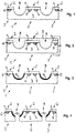
- a wafer 1 is provided with a multiplicity of structures 2, each for the electrical and / or optical function of the individual semiconductor chips 3 are required.
- the Structures 2 using known semiconductor technology methods produced, for example by means of mask technology, by sputtering and / or oxidizing the surface of the wafer 1.
- the structure 2 comprises the individual Semiconductor chips 3 each have an ion-selective field effect transistor, that into the silicon substrate 4 of the wafer 1 diffused drain and source zones 5, 6 with the substrate 4 opposite line type.
- Silicon dioxide layer 7 which the flat surface of the Forms wafers 1 and galvanically isolates them from the substrate 4.
- the outside facing away from the drain and source zones 5, 6 Surface of the silicon dioxide layer 7 forms an electrical active sensor layer, by means of which the field effect transistor Influence is controllable. So can the electrical conductivity between the drain zone 5 and the source zone 6, for example on the surface of silicon dioxide layer 7, in one Fluid contained ions are affected.
- Electrolyte 9 can, for example, sulfuric acid, oxalic acid or in Potassium permanganate dissolved in water can be used.
- an anodizing voltage is applied to the substrate 4 of the wafer 1, which can be, for example, a few volts.
- the insulation layer 10 is formed only on the side walls the semiconductor chips 3, since the electrically conductive semiconductor substrate 4 only comes into contact with the electrolyte 9 there.
- the semiconductor chips 3 can be separated, for example, by a Saw cuts were made in the groove-like recess 8, the width of this saw cut is smaller than the width of the Saw cut, with which the recess 8 in the semiconductor substrate 4 was introduced (Fig. 4).
- a Saw cuts were made in the groove-like recess 8
- the width of this saw cut is smaller than the width of the Saw cut, with which the recess 8 in the semiconductor substrate 4 was introduced (Fig. 4).
- an electrical insulating layer for example a plastic layer become.
- the electrical closes Insulation layer 10 is flush with that on the flat surface of the semiconductor chips 3 located silicon dioxide layer 7. The electrical insulation layer 10 will therefore survive via the electrically active, flat-sided surface of the semiconductor chips 3 avoided.
- the separation of the semiconductor chips 3 and the isolation of the side walls of the semiconductor chips 3 are carried out in one work step by means of anodic oxidation.
- an electrolyte 9 is deposited by saw cuts on the surface of the wafer 1 while exposing the side walls of the semiconductor chips 3.
- An anodizing voltage of a few volts is applied between the electrolyte 9 and the substrate 4 of the wafer 1. While the side walls of the semiconductor chips 3 are exposed, the electrolyte 9 oxidizes the substrate 4 which is already exposed on the side wall regions.
- the electrolyte 9 simultaneously cools the sawing tool 11. In FIG on another, already exposed side wall, an electrical insulation layer 10 is already formed.
Abstract
Description
Die Erfindung betrifft ein Verfahren zum Herstellen eines Halbleiterchips.The invention relates to a method for producing a Semiconductor chips.
Zum gleichzeitigen Herstellen einer Vielzahl von Halbleiterchips ist es aus der Praxis bereits bekannt, einen Wafer mit einer der Anzahl der herzustellenden Halbleiterchips entsprechenden Anzahl Strukturen zu versehen, die jeweils für die Funktion der einzelnen Halbleiterchips erforderlich sind. Die Strukturen werden mit aus derHalbleitertechnikbekanntenStrukturierungsverfahrenhergestellt, beispielsweise durch Auftragen einer Photomaske und anschließendes Naß- oder Trockenätzen des Wafers und/oder durch Bedampfen des Wafers. Nach Fertigstellung der Strukturen werden die einzelnen Halbleiterchips durch Zerteilen des Wafers von dem Waferverbund abgetrennt und vereinzelt.For the simultaneous production of a large number of semiconductor chips it is already known from practice to use a wafer with one of the Number of semiconductor chips to be produced corresponding number To provide structures, each for the function of the individual Semiconductor chips are required. The structures are made with of the structuring methods known in semiconductor technology, for example by applying a photomask and then Wet or dry etching of the wafer and / or by vapor deposition of the Wafers. After completion of the structures, the individual Semiconductor chips by dividing the wafer from the wafer composite separated and isolated.
Bei solchen Halbleiterchips besteht das Problem, daß die quer zur Chipebene angeordneten, aus elektrische leitendem Halbleitermaterial bestehenden Seitenwandungen des Halbleiterchips elektrisch isoliert werden müssen, damit die Funktion des Halbleiterchips gewährleistet ist. So kann beispielsweise eine nicht ausreichend isolierte Seitenwandung bei einem in MESA-Technik strukturierten Halbleiterchip dazu führen, daß Feuchtigkeit an die im inneren der MESA-Struktur befindlichen pn-Übergänge gelangt und dort Kriechströme zwischen den unterschiedlich dotierten Halbleiterschichten verursacht.With such semiconductor chips there is the problem that the transverse to Arranged chip level, made of electrically conductive semiconductor material existing side walls of the semiconductor chip electrically must be isolated so that the function of the semiconductor chip is guaranteed. For example, one may not be sufficient insulated side wall in a structured using MESA technology Semiconductor chip cause moisture to adhere to the inside of the MESA structure located pn junctions and there Leakage currents between the differently doped semiconductor layers caused.
Es ist zwar bereits bekannt, einen Halbleiterchip in ein Kunststoffgehäuse einzugießen, um den Halbleiterchip vor einem Kontakt mit Feuchtigkeit oder anderen elektrische leitfähigen Medien zu schützen. Bei bestimmten Anwendungen, wie beispielsweise bei Halbleiterchips, die als oberflächenaktive Sensoren ausgebildete Strukturen zum Messen von Ionenkonzentrationen in flüssigen Medien aufweisen, kommt jedoch eine vollständige Kapselung des Halbleiterchips nicht in Betracht. Bei solchen Halbleiterchips muß nämlich die flachseitige Oberfläche des Halbleiterchips für das zu untersuchende Medium zugänglich sein, damit die dort angeordnete oberflächenaktive Struktur mit dem zu untersuchenden Medium in Berührung gelangen kann. Entsprechendes gilt für Halbleiterchips, an deren Oberfläche biologische Zellen adhärent angelagert werden sollen, zum Beispiel um an den Zellen Messungen durchzuführen und/oder um die Zellen durch elektrische Felder zu stimulieren. Solche Halbleiterchips werden beispielsweise in sogenannten Bio-Sensoren verwendet.It is already known to place a semiconductor chip in a plastic housing pour in to the semiconductor chip before contact with Moisture or other electrically conductive media protect. In certain applications, such as Semiconductor chips that are designed as surface-active sensors Structures for measuring ion concentrations in liquid media have, however, comes a complete encapsulation of the semiconductor chip not considered. With such semiconductor chips, namely the flat side surface of the semiconductor chip for that too investigating medium be accessible so that the arranged there surface active structure with the medium to be examined in Can come into contact. The same applies to semiconductor chips, biological cells are adherently attached to their surface should, for example, to carry out measurements on the cells and / or to stimulate the cells through electrical fields. Such semiconductor chips are used, for example, in so-called bio sensors used.
Bei einem anderen aus der Praxis bekannten Verfahren zum Herstellen eines Halbleiterchips wird der Wafer zunächst mit den für die Funktion der einzelnen Halbleiterchips erforderlichen Strukturen versehen und danach werden in die flachseitige Oberfläche des Wafers rinnenartige Vertiefungen eingebracht, welche die einzelnen Halbleiterchips jeweils umgrenzen. Dann wird auf die die rinnenartigen Vertiefungen aufweisende Oberfläche des Wafers eine thermoplastische, elektrisch isolierende Kunststoffmasse aufgetragen und mit einem Rakel glattgezogen. Dabei füllt die Kunststoffmasse die Vertiefungen vollständig aus. Nach dem Aushärten der Kunststoffmasse wird der Wafer zum Vereinzeln und Abtrennen der Halbleiterchips aus dem Waferverbund im Bereich der Vertiefungen zerteilt. Die Halbleiterchips weisen dann an ihren Seitenflächen bereichsweise eine elektrisch isolierende Kunststoffschicht auf, die beispielsweise dort befindliche pn-Übergänge abdecken kann. Ein Nachteil dieses Verfahrens besteht darin, daß die thermoplastische Kunststoffmasse beim Auftragen auf den Wafer und beim Abziehen mit den Rakel außer mit den Vertiefungen auch mit der flachseitigen, der für die Funktion des Halbleiterchips erforderliche Struktur aufweisenden Oberfläche der Halbleiterchips in Berührung kommt, wobei es zu einer chemischen und/oder physikalischen Veränderung der Struktur kommen kann. Bei einem unvollständigen Entfernen des thermoplastischen Kunststoffmaterials von den außerhalb der Vertiefungen befindlichen Oberflächenbereichen des Halbleiterchips wird außerdem die nachfolgende Montage des Halbleiterchips auf einem Träger, beispielsweise durch Bonden, Löten oder Kleben wesentlich erschwert.In another method for manufacturing known from practice of a semiconductor chip, the wafer is first coated with that for the Function of the individual semiconductor chips required structures and then into the flat surface of the wafer channel-like depressions introduced, which the individual Limit semiconductor chips in each case. Then the gutter-like The surface of the wafer has depressions thermoplastic, electrically insulating plastic compound applied and smoothed with a squeegee. The fills up Plastic mass completely from the wells. After curing The plastic mass is used to separate and separate the wafer the semiconductor chips from the wafer composite in the area of the depressions divided. The semiconductor chips then have on their side faces an electrically insulating plastic layer in some areas, which can cover, for example, pn junctions located there. A disadvantage of this method is that the thermoplastic Plastic mass when applied to the wafer and when stripping with the squeegee not only with the recesses but also with the flat-sided the structure required for the function of the semiconductor chip surface of the semiconductor chips comes into contact, causing a chemical and / or physical change the structure can come. If the incomplete removal of the thermoplastic material from outside the Well-located surface areas of the semiconductor chip the subsequent assembly of the semiconductor chip on a Carrier, for example by bonding, soldering or gluing essential difficult.
Bei dem aus EP 0 148 687 A1 bekannten Verfahren wird auf einen Wafer eine Mesa-Struktur für einen als Photodiode ausgebildeten Halbleiterchip aufgebracht. Dabei wird der Wafer zunächst mit einer photoempfindlichen Schicht versehen und anschließend werden im Umgrenzungsbereich des Halbleiterchips dessen Seitenwandungen durch Einbringen von Mesagräben bereichsweise freigelegt. Danach wird die Oberfläche des Wafers durch anodische Oxidation mit einer Isolationsschicht versehen. Auf diese werden eine metallische Schicht, eine Schicht aus einem dielektrischen Material sowie elektrische Kontakte aufgebracht. Das Verfahrens hat den Nachteil, daß zum Verbinden der Anschlußkontakte mit der photoempfindlichen Schicht in die anodisch oxidierte Schicht und die dielektrische Schicht eine Öffnung eingebracht werden muß, wozu ein zusätzlicher Maskierungs- und Ätzschritt erforderlich ist. Ungünstig ist außerdem, daß nach dem Ablösen des Halbleiterchips von dem Wafer, das entlang der Talsohlen der Mesagräben erfolgt, die für die Funktion des Halbleiterchips erforderliche metallische Schicht an der Seitenfläche des Halbleiterchips freiliegt und dort nicht elektrisch isoliert ist.In the method known from EP 0 148 687 A1, a wafer is used a mesa structure for one designed as a photodiode Semiconductor chip applied. The wafer is first used with a provided photosensitive layer and then in Boundary area of the semiconductor chip whose side walls exposed by digging mesa trenches. After that is the surface of the wafer by anodic oxidation with a Insulation layer provided. On this become a metallic Layer, a layer of a dielectric material as well electrical contacts applied. The disadvantage of the process that to connect the contacts with the photosensitive Layer in the anodized layer and the dielectric Layer an opening must be made, for which an additional Masking and etching step is required. It is also unfavorable that after detaching the semiconductor chip from the wafer that along the bottom of the mesa trenches, which is necessary for the function of the Semiconductor chips required metallic layer on the side surface of the semiconductor chip is exposed and not electrically isolated there is.
Auch bei den aus CHANG, E.Y., et al., IR: IEEE Transactions an Semiconductor Manufactoring, Vol. 4, No. 1, 1991, S. 66-68 und US 4 839 300 bekannten Verfahren werden Seitenflächen eines Halbleiterchips freigelegt. Bei diesen Verfahren ist eine elektrische Isolation der freigelegten Seitenflächen nicht vorgesehen.Also in those from CHANG, E.Y., et al., IR: IEEE Transactions Semiconductor Manufactoring, Vol. 4, No. 1, 1991, pp. 66-68 and Methods known from US 4,839,300 are side surfaces of a Semiconductor chips exposed. In these processes, an electrical Insulation of the exposed side surfaces is not provided.
Man kennt auch bereits ein Verfahren zum Herstellen eines Halbleiterchips, bei dem vor dem Strukturieren des Wafers mit den für die Funktion der Halbleiterchips erforderlichen Strukturen in die flachseitige Oberfläche des Wafers zunächst rinnenartige Vertiefungen eingebracht werden und die Oberfläche des Wafers anschließend durch eine Temperaturbehandlung in einer sauerstoffhaltigen Atmosphäre mit einer elektrisch isolierenden Halbleiter-Oxid-Schicht versehen wird. Diese wird dann außerhalb der rinnenartigen Vertiefungen nach Aufbringen einer Lackmaske durch Ätzen entfernt. Anschließend werden die für die Funktion der Halbleiterchips erforderlichen Strukturen erzeugt. Dieses Verfahren hat jedoch den Nachteil, daß der Wafer bei der Herstellung der für die Funktion der Halbleiterchips erforderlichen Strukturen aufgrund der dann bereits vorhandenen Vertiefungen nur noch eine vergleichsweise geringe mechanische Stabilität aufweist. Bei den einzelnen, für die Strukturierung erforderlichen Bearbeitungsschritten und/oder beim Transport des Wafers zu den unterschiedlichen Bearbeitungsstationen kann es daher zu einer mechanischen Beschädigung des Wafers kommen, was bei einer fabrikmäßigen Herstellung der Halbleiterbauelemente zu nicht unerheblichen Produktionsausfallzeiten führen kann, beispielsweise wenn ein Wafer in einer Vakuumkammer zerbricht und die Vakuumkammer dann zum manuellen Entnehmen des Wafers belüftet werden muß. Ein weiterer Nachteil des Verfahrens besteht darin, daß die die Vertiefungen aufweisende Oberfläche des Wafers für eine Photolithographische Herstellung der für die Funktion der Halbleiterchips erforderlichen Struktur ungünstig gestaltet ist. So kann es beispielsweise beim Auftragen eines Photolacks auf den rotierenden Wafer nach dem sogenannten Schleuderverfahren zu einer ungleichmäßigen Ausbildung des Lackfilms kommen.A method for producing one is already known Semiconductor chips, in which before the wafer is structured with the structures required for the function of the semiconductor chips in the flat surface of the wafer is initially channel-like Wells are made and the surface of the wafer then by a temperature treatment in an oxygen-containing Atmosphere with an electrically insulating semiconductor oxide layer is provided. This will then be outside the channel-like depressions after applying a paint mask Etching removed. Then the for the function of the Semiconductor chips required structures generated. This method has the disadvantage, however, that the wafer in the manufacture of the for structures required due to the function of the semiconductor chips of the existing wells then only a comparative one has low mechanical stability. With the individual, processing steps required for structuring and / or when transporting the wafer to the different processing stations can therefore cause mechanical damage to the wafer come what a factory manufacture of the semiconductor devices lead to considerable downtimes in production can, for example, if a wafer breaks in a vacuum chamber and the vacuum chamber for manual removal of the wafer must be ventilated. Another disadvantage of the method is in that the recessed surface of the wafer for a photolithographic production of the for the function of the Semiconductor chips required structure is designed unfavorably. For example, when applying a photoresist to the rotating wafer after the so-called spin process to a uneven formation of the paint film come.
Aus DE 43 05 296 C2 ist ferner ein Verfahren zum Herstellen von Halbleiterchips in Mesa-Technik bekannt, bei dem auf einem Wafer zuerst die für die Funktion der Halbleiterchips jeweils erforderlichen Strukturen erzeugt werden. Danach werden im Umgrenzungsbereich der Halbleiterchips deren Seitenwandungen durch Einbringen von Mesagräben in den Wafer bereichsweise freigelegt. Anschließend wird auf die flachseitige Oberfläche des Wafers durch CVD-Oxidation eine Siliziumdioxid-Schicht aufgebracht. Danach werden die mit ihrer der Struktur abgewandten Rückseiten an einer Trägerfolie anhaftenden Halbleiterchips durch Sägeschnitte entlang der Talsohlen der Mesagräben vom Wafer abgetrennt. Dabei wird die Trägerfolie nicht durchtrennt. Die nach dem Sägen weiterhin an der Trägerfolie anhaftenden Halbleiterchips werden mit einem Ätzmittel in Berührung gebracht, um die durch die Sägeschnitte freigelegten Seitenwandungen der Halbleiterchips aufzurauhen. Anschließend wird in einem weiteren Fertigungsschritt die Siliziumdioxid-Schicht, welche die für die Funktion der Halbleiterchips erforderlichen Strukturen vor dem Angriff des Ätzmittels geschützt hat, entfernt. Das Verfahren hat den Nachteil, daß die elektrisch leitfähigen Bereiche der für die Funktion des jeweiligen Halbleiterchips erforderlichen Struktur nach Fertigstellung des Halbleiterchips freiligen und elektrisch nicht isoliert sind.DE 43 05 296 C2 also describes a method for producing Semiconductor chips known in mesa technology, in which on a wafer first of all those required for the function of the semiconductor chips Structures are created. Then be in the boundary area the semiconductor chips whose side walls by introducing areas of mesa trenches exposed in the wafer. Subsequently is applied to the flat surface of the wafer by CVD oxidation applied a silicon dioxide layer. After that, they are with their backs of the structure facing away adhering to a carrier film Semiconductor chips through saw cuts along the valley bottoms of the Mesa trenches separated from the wafer. The carrier film is not severed. After sawing continue on the carrier film adhering semiconductor chips are in contact with an etchant brought to the side walls exposed by the saw cuts to roughen the semiconductor chips. Then in another Manufacturing step the silicon dioxide layer, which the for the Function of the semiconductor chips required structures before Has protected attack of the etchant removed. The procedure has the disadvantage that the electrically conductive areas for the Function of the respective semiconductor chip required structure after completion of the semiconductor chip release and electrical are not isolated.
Es besteht deshalb die Aufgabe, ein Verfahren der eingangs genannten Art zu schaffen, das eine einfache Herstellung eines Halbleiterchips ermöglicht. Außerdem soll beim Aufbringen der Isolationsschicht auf die Seitenwandungen des Halbleiterchips eine Beeinträchtigung der für die Funktion des Halbleiterchips erforderlichen Struktur vermieden werden.There is therefore the task of a method of the aforementioned Kind of creating a simple manufacture of a semiconductor chip enables. In addition, when applying the insulation layer an impairment on the side walls of the semiconductor chip the structure required for the function of the semiconductor chip be avoided.
Diese Aufgabe wird mit den Merkmalen des Patentanspruchs 1 gelöst. This object is achieved with the features of
Bei dem erfindungsgemäßen Verfahren wird der Wafer also zunächst mit den für die elektrische Funktion des Halbleiterchips erforderlichen Struktur versehen, die beispielsweise einen oberflächenaktiven Sensor, einen Transistor, eine Elektrode und/oder einen Interdigitalkondensator umfassen kann. Danach werden quer zur Erstreckungsebene des Halbleiterchips angeordnete Seitenwandungen des Halbleiterchips zumindest bereichsweise freigelegt. Zum anodischen Oxidieren der Oberfläche dieser Seitenwandungen wird der Halbleiterchip mit einem Elektrolyten in Verbindung gebracht, beispielsweise mit Schwefelsäure, Oxalsäure oder in Wasser gelöstem Kaliumpermanganat. Dabei wird zwischen dem Elektrolyt und dem an den Seitenwandungen freiliegenden, elektrisch leitfähigen Halbleitersubstrat eine Anodisierspannung angelegt.In the method according to the invention, the wafer is therefore initially with those required for the electrical function of the semiconductor chip Structure provided, for example, a surface active sensor, a transistor, an electrode and / or an interdigital capacitor. After that are arranged transversely to the plane of extent of the semiconductor chip Side walls of the semiconductor chip at least in regions exposed. For anodizing the surface of this The semiconductor chip is coated with side walls with an electrolyte Connected, for example with sulfuric acid, oxalic acid or potassium permanganate dissolved in water. It is between the Electrolyte and the exposed on the side walls, electrical conductive semiconductor substrate applied an anodizing voltage.
Bei dem erfindungsgemäßen Verfahren ist der Wafer bzw. der daraus hergestellte Halbleiterchip sowohl vor als auch nach dem Aufbringen der elektrischen Isolationsschicht gut prozessierbar. Da die anodische Oxydation des Wafers nur an den elektrisch leitfähigen Seitenflächen des Wafers erfolgt, ist das Verfahren selbstjustierend, d.h. die Beschichtung erfolgt nur dort, wo sie erwünscht ist. Bei Halbeiterchips, die eine elektrisch oberflächenaktive Struktur aufweisen (z.B. Sensoren), wird dadurch beim Beschichten der Seitenwandungen des Halbleiterchips mit der elektrischen Isolationsschicht eine Beeinträchtigung der oberflächenaktiven Struktur oder deren Funktion vermieden. Da die anodische Oxydation bei Raumtemperatur durchgeführt werden kann, entfällt außerdem eine Schädigung der elektrisch aktiven Halbleiter-Strukturen durch Wärmebehandlung. Gegenüber einer mechanisch aufgebrachten Isolationsschicht weist die durch anodische Oxydation hergestellte Isolationsschicht außerdem eine bessere Feuchtigkeitsbeständigkeit auf, da die Isolationsschicht durch chemische Umwandlung aus dem Halbleitermaterial selbst hergestellt ist und deshalb besonders gut mit diesem verbunden ist. Das erfindungsgemäße Verfahren ist zudem einfach durchführbar. In the method according to the invention, the wafer or the one made of it manufactured semiconductor chip both before and after application the electrical insulation layer is easy to process. Since the anodic oxidation of the wafer only on the electrically conductive Side of the wafer, the process is self-aligning, i.e. the coating is only carried out where it is required is. For semiconductor chips that have an electrically surface active Having structure (e.g. sensors) the side walls of the semiconductor chip with the electrical Isolation layer an impairment of the surface active Structure or its function avoided. Because the anodic oxidation can also be carried out at room temperature Damage to the electrically active semiconductor structures Heat treatment. Opposite a mechanically applied one Insulation layer shows the one produced by anodic oxidation Insulation layer also better moisture resistance on because the insulation layer is made by chemical conversion the semiconductor material itself is made and therefore special is well connected with this. The method according to the invention is also easy to carry out.
Eine Ausführungsform der Erfindung sieht vor, daß die Seitenwandungen des Halbleiterchips durch Einbringen einer rinnenartigen Vertiefung in eine flachseitige Oberfläche des Wafers freigelegt wird, daß der Wafer danach an den Seitenwandungen anodisch oxidiert wird und daß der Wafer anschließend zum Abtrennen des Halbleiterchips vom Wafer entlang der den Halbleiterchip umgrenzenden rinnenartigen Vertiefung zerteilt wird. Bei dieser Ausführungsform des Verfahrens werden vorzugsweise zunächst sämtliche, die auf dem Wafer befindlichen Halbleiterchips umgrenzende Vertiefungen in die Oberfläche des Wafers eingebracht und erst danach wird der Wafer mit dem Elektrolyten in Verbindung gebracht, beispielsweise indem der Elektrolyt an der Waferoberfläche deponiert wird. Die Isolierschichten an den einzelnen, die Halbleiterchips jeweils umgrenzenden Vertiefungen weisen dadurch jeweils die gleiche Schichtdicke auf. Außerdem bleibt der Waferverbund während des anodischen Oxidierens der Seitenwandungen des Halbleiterchips erhalten.An embodiment of the invention provides that the side walls the semiconductor chip by introducing a groove-like depression that is exposed in a flat surface of the wafer the wafer is then anodized on the side walls and that the wafer is then used to separate the semiconductor chip from the Wafers along the trough-like surrounding the semiconductor chip Deepening is divided. In this embodiment of the method are preferably all that are on the wafer semiconductor chips located in the recesses Surface of the wafer is introduced and only then is the wafer associated with the electrolyte, for example by the electrolyte is deposited on the wafer surface. The Insulating layers on the individual, the semiconductor chips each delimiting depressions each have the same Layer thickness. In addition, the wafer composite remains during the anodizing the side walls of the semiconductor chip receive.
Bei einer vorteilhaften Ausführungsform des Verfahrens erfolgt das Freilegen der anodisch zu oxidierenden Seitenwandungen und/oder das Zerteilen des Wafers entlang der den Halbleiterchip seitlich begrenzenden rinnenartigen Vertiefung durch mechanisches Abtragen von Wafermaterial. Dabei wird das Wafermaterial vorzugsweise durch Sägen abgetragen. Dadurch kann das Auftragen einer Maske und ein umständliches Ätzen der rinnenartigen Vertiefungen entfallen.In an advantageous embodiment of the method exposing the side walls to be anodized and / or dicing the wafer along the side of the semiconductor chip delimiting groove-like depression by mechanical removal of wafer material. The wafer material is preferably through Saws removed. This can make applying a mask and a cumbersome etching of the channel-like depressions is no longer necessary.
Vorteilhaft ist, wenn auf die beim Zerteilen des Wafers im Bereich der rinnenartigen Vertiefungen an dem Halbleiterchip freigelegten Trennflächen eine elektrisch isolierende Schicht aufgebracht wird. Die Seitenflächen des Halbleiterchips können dadurch vollständig elektrisch isoliert werden. Dabei kann die isolierende Schicht gegebenenfalls die anodisch oxidierte Isolationsschicht bereichsweise überdecken. Die Feuchtigkeitsbeständigkeit des Halbleiterchips wird dadurch verbessert. It is advantageous if on cutting the wafer in the area of the groove-like depressions on the semiconductor chip Partitions an electrically insulating layer applied becomes. The side surfaces of the semiconductor chip can thereby be completely electrically isolated. The insulating Layer optionally the anodized insulation layer cover areas. The moisture resistance of the This improves semiconductor chips.
Bei einer besonders vorteilhaften Ausführungsform der Erfindung wird der Wafer zum gleichzeitigen Freiliegen und anodischen Oxidieren der Seitenwandungen des Halbleiterchips während des Freilegens der Seitenwandungen mit einem Elektrolyten in Verbindung gebracht. Dieser kann dann gleichzeitig auch als Kühlmittel für ein mechanisches Abtragungswerkzeug, beispielsweise ein Sägeblatt dienen.In a particularly advantageous embodiment of the invention the wafer becomes exposed and anodized simultaneously the side walls of the semiconductor chip during the exposure of the Sidewalls associated with an electrolyte. This can then also be used as a coolant for a mechanical removal tool, such as a saw blade.
Bei einer Ausführungsform der Erfindung ist vorgesehen, daß bevor der Halbleiterchip mit dem Elektrolyten in Verbindung gebracht wird, die für die Funktion des Halbleiterchips erforderliche Struktur elektrisch isoliert und/oder mit einer gegen den Elektrolyten chemisch beständigen Schicht versehen wird. Zum elektrischen Isolieren der Oberfläche der Struktur kann beispielsweise in üblicher Weise eine Siliziumdioxid-Schicht auf dem Halbleiterchip aufgebracht werden.In one embodiment of the invention it is provided that before the semiconductor chip is connected to the electrolyte, the structure required for the function of the semiconductor chip electrically isolated and / or with one against the electrolyte chemically resistant layer is provided. For electrical Isolating the surface of the structure can, for example, in the usual Way a silicon dioxide layer applied to the semiconductor chip become.
Der Halbleiterchip kann nach dem Herstellen der Isolationsschicht in eine an den Halbleiterchip formangepaßte Aufnahme eines vorzugsweise optisch transparenten Trägerplättchens eingesetzt werden, wobei der Halbleiterchip mit einer wenigstens eine als oberflächenaktiver Sensor ausgebildete Struktur aufweisenden flachseitigen Oberfläche in der Oberflächenebene einer an die Aufnahme angrenzenden flachseitigen Oberfläche des Trägerplättchens angeordnet wird. Ein solcher Halbleiterchip kann beispielsweise als mikroskopierbarer Biosensor verwendet werden, indem auf der in einer Ebene mit der Oberlächenebene des Trägerplättchens angeordneten flachseitigen Oberfläche des Halbleiterchips biologische Zellen in einem Nährmedium adhärent angelagert werden. Die Zellen können dann durch ein Mikroskop optisch beobachtet werden und gleichzeitig können mittels der auf dem Halbleiterchip befindlichen Strukturen Messungen an den Zellen und/oder dem Nährmedium durchgeführt werden. Da die an den Seitenwandungen befindliche Isolationsschicht durch anodische Oxidation des Halbleitermaterials hergestellt wird, wird ein Überstehen der Isolationsschicht über die flachseitige Oberflächenebene des Halbleiterchips vermieden. Somit ergibt sich an der Oberfläche des Halbleiterchips eine ebene Fläche ohne Überstände, die eine Fortsetzung der Oberflächenebene des Trägerplättchens bildet. Biologische Zellen können sich dann besonders gut an der Oberfläche des Halbleiterchips und des Trägersplättchens anlagern.The semiconductor chip can be produced after the insulation layer into a receptacle of a shape adapted to the semiconductor chip preferably optically transparent carrier plate used be, the semiconductor chip having at least one as Surface-active sensor trained structure flat surface in the surface plane one to the Recording adjacent flat surface of the carrier plate is arranged. Such a semiconductor chip can, for example can be used as a microscopic biosensor by using the in one plane with the surface plane of the carrier plate arranged flat-side surface of the semiconductor chip biological cells are adherently attached in a nutrient medium. The cells can then be observed optically through a microscope be and at the same time by means of on the semiconductor chip existing structures measurements on the cells and / or the Culture medium are carried out. Because the on the side walls insulation layer by anodic oxidation of the Semiconductor material is produced, will survive the Insulation layer over the flat surface surface of the Semiconductor chips avoided. Thus on the surface of the Semiconductor chips a flat surface without protrusions, the one Continuation of the surface plane of the carrier plate forms. Biological cells can then be particularly good on the surface attach the semiconductor chip and the carrier plate.
Nachfolgend sind Ausführungsbeispiele der Erfindung anhand der Zeichnung näher erläutert. Es zeigen:
- Fig. 1
- einen Querschnitt durch einen Wafer, in dessen elektrisch aktive Oberfläche Vertiefungen eingebracht wurden, welche die Seitenwandungen von Halbleiterchips bereichsweise freilegen,
- Fig. 2
- der in Fig. 1 gezeigte Wafer beim anodischen Oxidieren der Seitenwandungen der Halbleiterchips,
- Fig. 3
- eine Darstellung ähnlich Fig. 1, wobei jedoch die Seitenwandungen des Halbleiterchips eine oberflächennahe anodische Oxidationsschicht als elektrische Isolation aufweisen,
- Fig. 4
- der in Fig. 3 gezeigte Wafer nach dem Heraustrennen der Halbleiterchips aus dem Waferverbund und
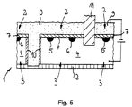
- Fig. 5
- einen Wafer, bei dem die Seitenwandungen der Halbleiterchips während des Freilegens der Seitenflächen anodisch oxidiert werden.
- Fig. 1
- 3 shows a cross section through a wafer, in the electrically active surface of which recesses have been made which expose the side walls of semiconductor chips in regions,
- Fig. 2
- 1 during anodic oxidation of the side walls of the semiconductor chips,
- Fig. 3
- 1, but the side walls of the semiconductor chip have a near-surface anodic oxidation layer as electrical insulation,
- Fig. 4
- 3 after the semiconductor chips have been removed from the wafer composite and
- Fig. 5
- a wafer in which the side walls of the semiconductor chips are anodically oxidized during the exposure of the side surfaces.
Bei einem Verfahren zum Herstellen einer Vielzahl von Halbleiterchips
wird ein Wafer 1 mit einer Vielzahl von Strukturen 2 versehen,
die jeweils für die elektrische und/oder optische Funktion der
einzelnen Halbleiterchips 3 erforderlich sind. Dabei werden die
Strukturen 2 mit an sich bekannten Methoden der Halbleitertechnik
hergestellt, beispielsweise mittels Maskentechnik, durch Sputtern
und/oder Oxidieren der Oberfläche des Wafers 1.In a method of manufacturing a plurality of semiconductor chips
a
Wie aus Fig. 1 erkennbar ist, umfaßt die Struktur 2 der einzelnen
Halbleiterchips 3 jeweils einen ionenselektiven Feldeffekttransistor,
der in das Silicium-Substrat 4 des Wafers 1
diffundierte Drain- und Source-Zonen 5, 6 mit zu dem Substrat 4
entgegengesetztem Leitungstyp aufweist. Darüber befindet sich eine
Silicumdioxid-Schicht 7, welche die flachseitige Oberfläche des
Wafers 1 bildet und diese galvanisch gegen das Substrat 4 isoliert.
Die den Drain- und Source-Zonen 5, 6 abgewandte außenseitige
Oberfläche der Siliciumdioxid-Schicht 7 bildet eine elektrisch
aktive Sensorschicht, mittels welcher der Feldeffekttransistor durch
Influenz steuerbar ist. So kann die elektrische Leitfähigkeit
zwischen der Drain-Zone 5 und der Source-Zone 6 beispielsweise durch
an der Oberfläche Siliciumdioxid-Schicht 7 befindliche, in einem
Fluid enthaltene Ionen beeinflußt werden.As can be seen from Fig. 1, the
Nach dem Herstellen der für die Funktion der Halbleiterchips 3
erforderlichen Strukturen 2 werden im Umgrenzungsbereich der
Halbleiterchips 3 deren Seitenwandungen durch Einbringen von
rinnenartigen Vertiefungen 8 in die benachbart zu den Strukturen
2 angeordnete flachseitige Oberfläche des Wafers 1 mittels eines
Sägewerkzeuges freigelegt. Dann wird an der Oberfläche des Wafers
1 ein die Vertiefungen 8 ausfüllender Elektrolyt 9 deponiert. Als
Elektrolyt 9 kann beispielsweise Schwefelsäure, Oxalsäure oder in
Wasser gelöstes Kaliumpermanganat verwendet werden. Zum
anodischen Oxidieren der durch die Vertiefungen 8 freigelegten
Seitenwandungen der Halbleiterchips 3 wird zwischen dem Elektrolyt
9 und dem Substrat 4 des Wafers 1 eine Anodisierspannung angelegt,
die beispielsweise einige Volt betragen kann. Nach einer Zeit von
einigen Minuten ist die an der Oberfläche der Seitenwandung
befindliche Halbleiterschicht in eine anodische Oxidschicht
umgewandelt, das eine elektrische Isolationsschicht 10 bildet. Dabei
bildet sich die Isolationsschicht 10 nur an den Seitenwandungen
der Halbleiterchips 3, da das elektrisch leitfähige Halbleiter-Substrat
4 nur dort mit dem Elektrolyten 9 in Berührung kommt. Die
im Bereich der Strukturen 2 befindliche, die Siliciumdioxid-Schicht
7 aufweisende flachseitige Oberfläche des Wafers 1 wird dagegen
durch den Elektrolyten 9 nicht verändert.After the production of the function of the
Nach dem Fertigstellen der Isolationsschichten 10 werden die
Halbleiterchips 3 durch Zertrennen des Wafers 1 entlang der
rinnenartigen Vertiefungen 8 von dem Waferverbund abgelöst. Das
Vereinzeln der Halbleiterchips 3 kann beispielsweise durch einen
Sägeschnitt in der rinnenartigen Vertiefung 8 erfolgten, wobei die
breite dieses Sägeschnitts kleiner ist als die breite des
Sägeschnitts, mit dem die Vertiefung 8 in das Halbleitersubstrat
4 eingebracht wurde (Fig. 4). Die beim Vereinzeln der Halbleiterchips
3 im Bereich der rinnenartigen Vertiefung 8 entstehende Trennfläche
kann gegebenenfalls durch Aufbringen einer elektrisch
isolierenden Schicht, zum Beispiel einer Kunststoffschicht isoliert
werden. Wie aus Fig. 4 erkennbar ist, schließt die elektrische
Isolationsschicht 10 bündig mit der an der flachseitigen Oberfläche
der Halbleiterchips 3 befindlichen Siliciumdioxid-Schicht 7 ab.
Es wird also ein Überstehen der elektrischen Isolationsschicht 10
über die elektrisch aktive, flachseitige Oberfläche der Halbleiterchips
3 vermieden.After the completion of the insulation layers 10
Bei dem in Fig. 5 gezeigten Ausführungsbeispiel wird das Vereinzeln
der Halbleiterchips 3 und das Isolieren der Seitenwandungen der
Halbleiterchips 3 mittels anodischer Oxydation in einem Arbeitsschritt
durchgeführt. An der Oberfläche des Wafers 1 wird dazu
während des Freilegens der Seitwandungen der Halbleiterchips 3 durch
Sägeschnitte ein Elektrolyt 9 deponiert. Zwischen dem Elektrolyt
9 und dem Substrat 4 des Wafers 1 wird eine Anodisierspannung von
einigen Volt angelegt. Während des Freiliegens der Seitenwandungen
der Halbleiterchips 3 oxidiert der Elektrolyt 9 das an bereits
freigelegten Seitwandungsbereichen befindliche Substrat 4. Der
Elektrolyt 9 bewirkt gleichzeitig eine Kühlung des Sägewerkzeugs
11. In Fig. 5 ist deutlich erkennbar, daß während des Freilegens
einer der Seitenwandungen eines Halbleiterchips 3 an einer anderen,
bereits freigelegten Seitenwandung bereits eine elektrische
Isolationsschicht 10 gebildet ist.
Erwähnt werden soll noch, daß der Wafer 1 während des anodischen
Oxidierens der Isolationsschicht 10 mit seiner der Struktur 2
abgewandten Rückseite an einer Haftfolie 12 anhaftet, welche die
Rückseite des Wafers 1 gegen den Elektrolyten 9 abdichtet. Die
Haftfolie 12 wird beim Vereinzeln der Halbleiterchips 3 von diesen
abgelöst.In the exemplary embodiment shown in FIG. 5, the separation of the
It should also be mentioned that during the anodic oxidation of the
Claims (6)
Applications Claiming Priority (2)
| Application Number | Priority Date | Filing Date | Title |
|---|---|---|---|
| DE19848460 | 1998-10-21 | ||
| DE19848460A DE19848460A1 (en) | 1998-10-21 | 1998-10-21 | Semiconductor component and method for producing a semiconductor chip |
Publications (1)
| Publication Number | Publication Date |
|---|---|
| EP0996147A1 true EP0996147A1 (en) | 2000-04-26 |
Family
ID=7885142
Family Applications (1)
| Application Number | Title | Priority Date | Filing Date |
|---|---|---|---|
| EP99120334A Withdrawn EP0996147A1 (en) | 1998-10-21 | 1999-10-12 | Manufacturing method for semiconductor chips using anodic oxidation |
Country Status (3)
| Country | Link |
|---|---|
| EP (1) | EP0996147A1 (en) |
| JP (1) | JP2000133650A (en) |
| DE (1) | DE19848460A1 (en) |
Cited By (3)
| Publication number | Priority date | Publication date | Assignee | Title |
|---|---|---|---|---|
| DE10138981A1 (en) * | 2001-08-08 | 2003-03-06 | Infineon Technologies Ag | Process for the electrochemical oxidation of a semiconductor substrate |
| DE10216614A1 (en) * | 2002-04-15 | 2003-10-30 | Infineon Technologies Ag | Production of a thin dielectric layer on a conducting substrate used in the semiconductor industry comprises applying a thin dielectric layer on the substrate, placing in an electrochemical cell, and applying an electrical potential |
| WO2020254499A1 (en) * | 2019-06-21 | 2020-12-24 | Infineon Technologies Austria Ag | Method of manufacturing semiconductor chips having a side wall sealing |
Families Citing this family (3)
| Publication number | Priority date | Publication date | Assignee | Title |
|---|---|---|---|---|
| JP4927343B2 (en) * | 2005-03-18 | 2012-05-09 | ルネサスエレクトロニクス株式会社 | Semiconductor chip and manufacturing method thereof |
| JP2009252998A (en) * | 2008-04-07 | 2009-10-29 | Sanyo Electric Co Ltd | Semiconductor light emitting element and method of manufacturing the same |
| JP6387244B2 (en) * | 2014-05-13 | 2018-09-05 | 株式会社ディスコ | Wafer processing method |
Citations (2)
| Publication number | Priority date | Publication date | Assignee | Title |
|---|---|---|---|---|
| DE4305296A1 (en) * | 1993-02-20 | 1994-08-25 | Telefunken Microelectron | Radiation-emitting diode with improved radiation power |
| US5559058A (en) * | 1994-11-15 | 1996-09-24 | Peter S. Zory, Jr. | Method for producing native oxides on compound semiconductors |
Family Cites Families (2)
| Publication number | Priority date | Publication date | Assignee | Title |
|---|---|---|---|---|
| FR2557371B1 (en) * | 1983-12-27 | 1987-01-16 | Thomson Csf | PHOTOSENSITIVE DEVICE COMPRISING BETWEEN THE DETECTORS OF THE RADIATION OPAQUE AREAS TO BE DETECTED, AND MANUFACTURING METHOD |
| JPH0740609B2 (en) * | 1985-12-20 | 1995-05-01 | セイコー電子工業株式会社 | Method for manufacturing semiconductor device |
-
1998
- 1998-10-21 DE DE19848460A patent/DE19848460A1/en not_active Withdrawn
-
1999
- 1999-10-12 EP EP99120334A patent/EP0996147A1/en not_active Withdrawn
- 1999-10-19 JP JP11296919A patent/JP2000133650A/en active Pending
Patent Citations (2)
| Publication number | Priority date | Publication date | Assignee | Title |
|---|---|---|---|---|
| DE4305296A1 (en) * | 1993-02-20 | 1994-08-25 | Telefunken Microelectron | Radiation-emitting diode with improved radiation power |
| US5559058A (en) * | 1994-11-15 | 1996-09-24 | Peter S. Zory, Jr. | Method for producing native oxides on compound semiconductors |
Non-Patent Citations (1)
| Title |
|---|
| "Semiconductor Chip Insulation by Anodic Oxidation", IBM TECHNICAL DISCLOSURE BULLETIN, vol. 7, no. 6, November 1964 (1964-11-01), US, pages 528 - 529, XP002125071 * |
Cited By (7)
| Publication number | Priority date | Publication date | Assignee | Title |
|---|---|---|---|---|
| DE10138981A1 (en) * | 2001-08-08 | 2003-03-06 | Infineon Technologies Ag | Process for the electrochemical oxidation of a semiconductor substrate |
| US6559069B2 (en) | 2001-08-08 | 2003-05-06 | Infineon Technologies Ag | Process for the electrochemical oxidation of a semiconductor substrate |
| DE10138981B4 (en) * | 2001-08-08 | 2005-09-08 | Infineon Technologies Ag | A method of forming silicon oxide by electrochemical oxidation of a well semiconductor substrate |
| DE10216614A1 (en) * | 2002-04-15 | 2003-10-30 | Infineon Technologies Ag | Production of a thin dielectric layer on a conducting substrate used in the semiconductor industry comprises applying a thin dielectric layer on the substrate, placing in an electrochemical cell, and applying an electrical potential |
| DE10216614B4 (en) * | 2002-04-15 | 2004-06-17 | Infineon Technologies Ag | Method for reinforcing a dielectric layer on a semiconductor substrate at defects and arrangement with a reinforced dielectric layer |
| US7176514B2 (en) | 2002-04-15 | 2007-02-13 | Infineon Technologies Ag | Method and configuration for reinforcement of a dielectric layer at defects by self-aligning and self-limiting electrochemical conversion of a substrate material |
| WO2020254499A1 (en) * | 2019-06-21 | 2020-12-24 | Infineon Technologies Austria Ag | Method of manufacturing semiconductor chips having a side wall sealing |
Also Published As
| Publication number | Publication date |
|---|---|
| DE19848460A1 (en) | 2000-05-04 |
| JP2000133650A (en) | 2000-05-12 |
Similar Documents
| Publication | Publication Date | Title |
|---|---|---|
| DE3021206C2 (en) | Process for the production of conductor tracks on semiconductor components | |
| DE69836451T2 (en) | Microelectronic structure of a difficult to etch material and metallized holes | |
| DE1930669C2 (en) | Method for manufacturing an integrated semiconductor circuit | |
| DE4130555C2 (en) | Semiconductor device with high breakdown voltage and low resistance, and manufacturing method | |
| DE2901697B2 (en) | Method for forming connecting lines on a substrate | |
| DE1961634B2 (en) | METHOD OF MANUFACTURING A METAL ISOLATOR SEMICONDUCTOR FIELD EFFECT TRANSISTOR | |
| DE1803024A1 (en) | Integrated semiconductor device and method for its manufacture | |
| DE2736200A1 (en) | CHEMICALLY SENSITIVE FIELD EFFECT TRANSISTOR AND METHOD FOR MANUFACTURING THE SAME | |
| DE2620998A1 (en) | METHOD FOR MANUFACTURING CARRIERS FOR PROCESSING IC CHIPS | |
| EP0996147A1 (en) | Manufacturing method for semiconductor chips using anodic oxidation | |
| DE1231812B (en) | Process for the production of electrical semiconductor components according to the mesa diffusion technique | |
| DE102017200952B4 (en) | Semiconductor device and method of manufacturing a semiconductor device | |
| DE3145101C2 (en) | Method for manufacturing a semiconductor memory | |
| DE4310205C1 (en) | Prodn. of hole structure in silicon substrate - by producing pores in substrate by etching, forming mask on substrate and selectively etching | |
| DE10350036A1 (en) | Method for separating semiconductor chips and corresponding semiconductor chip arrangement | |
| DE3128629A1 (en) | RESET PROCESS FOR INTEGRATED CIRCUITS | |
| EP0028786B1 (en) | Ion implantations method | |
| DE10244077B4 (en) | Process for the production of semiconductor devices with plated through-hole | |
| DE1908901C3 (en) | Process for the production of semiconductor components with small dimensions | |
| WO1993017459A2 (en) | Process for producing a semiconductor structure and semiconductor structure produced according to this process | |
| DE2224468A1 (en) | Etching glass/silica coatings - using carbon tetrafluoride plasma and photoresist mask | |
| DE102009010891A1 (en) | Method for producing MOSFET contacts on surface of silicon carbide semiconductor material of e.g. semiconductor element, involves heating metal layer to specific temperature, and removing metal layer from region of insulation layer | |
| DE4430812C1 (en) | Prodn. of ion-sensitive FET with contact at back | |
| WO2002050878A1 (en) | Method for producing a solid body comprising a microstructure | |
| WO2019030040A1 (en) | Micromechanical device and corresponding production method |
Legal Events
| Date | Code | Title | Description |
|---|---|---|---|
| PUAI | Public reference made under article 153(3) epc to a published international application that has entered the european phase |
Free format text: ORIGINAL CODE: 0009012 |
|
| 17P | Request for examination filed |
Effective date: 20000219 |
|
| AK | Designated contracting states |
Kind code of ref document: A1 Designated state(s): CH DE FR GB IT LI NL |
|
| AX | Request for extension of the european patent |
Free format text: AL;LT;LV;MK;RO;SI |
|
| RAP1 | Party data changed (applicant data changed or rights of an application transferred) |
Owner name: MICRONAS GMBH |
|
| 17Q | First examination report despatched |
Effective date: 20000803 |
|
| AKX | Designation fees paid |
Free format text: CH DE FR GB IT LI NL |
|
| STAA | Information on the status of an ep patent application or granted ep patent |
Free format text: STATUS: THE APPLICATION IS DEEMED TO BE WITHDRAWN |
|
| 18D | Application deemed to be withdrawn |
Effective date: 20010214 |