EP0987652B1 - IC-Karte und Herstellungsverfahren derselben - Google Patents
IC-Karte und Herstellungsverfahren derselben Download PDFInfo
- Publication number
- EP0987652B1 EP0987652B1 EP99307396A EP99307396A EP0987652B1 EP 0987652 B1 EP0987652 B1 EP 0987652B1 EP 99307396 A EP99307396 A EP 99307396A EP 99307396 A EP99307396 A EP 99307396A EP 0987652 B1 EP0987652 B1 EP 0987652B1
- Authority
- EP
- European Patent Office
- Prior art keywords
- chip
- card
- mirror surface
- dicing
- manufacturing
- Prior art date
- Legal status (The legal status is an assumption and is not a legal conclusion. Google has not performed a legal analysis and makes no representation as to the accuracy of the status listed.)
- Expired - Lifetime
Links
Images


Classifications
-
- G—PHYSICS
- G06—COMPUTING OR CALCULATING; COUNTING
- G06K—GRAPHICAL DATA READING; PRESENTATION OF DATA; RECORD CARRIERS; HANDLING RECORD CARRIERS
- G06K19/00—Record carriers for use with machines and with at least a part designed to carry digital markings
- G06K19/06—Record carriers for use with machines and with at least a part designed to carry digital markings characterised by the kind of the digital marking, e.g. shape, nature, code
- G06K19/067—Record carriers with conductive marks, printed circuits or semiconductor circuit elements, e.g. credit or identity cards also with resonating or responding marks without active components
- G06K19/07—Record carriers with conductive marks, printed circuits or semiconductor circuit elements, e.g. credit or identity cards also with resonating or responding marks without active components with integrated circuit chips
- G06K19/077—Constructional details, e.g. mounting of circuits in the carrier
- G06K19/0772—Physical layout of the record carrier
- G06K19/07728—Physical layout of the record carrier the record carrier comprising means for protection against impact or bending, e.g. protective shells or stress-absorbing layers around the integrated circuit
-
- G—PHYSICS
- G06—COMPUTING OR CALCULATING; COUNTING
- G06K—GRAPHICAL DATA READING; PRESENTATION OF DATA; RECORD CARRIERS; HANDLING RECORD CARRIERS
- G06K19/00—Record carriers for use with machines and with at least a part designed to carry digital markings
- G06K19/06—Record carriers for use with machines and with at least a part designed to carry digital markings characterised by the kind of the digital marking, e.g. shape, nature, code
- G06K19/067—Record carriers with conductive marks, printed circuits or semiconductor circuit elements, e.g. credit or identity cards also with resonating or responding marks without active components
- G06K19/07—Record carriers with conductive marks, printed circuits or semiconductor circuit elements, e.g. credit or identity cards also with resonating or responding marks without active components with integrated circuit chips
- G06K19/077—Constructional details, e.g. mounting of circuits in the carrier
Definitions
- IC cards Integrated Circuit cards
- IC cards can have the following features.
- a card is put in a purse, a card case or carried loose whether it is an IC card or a magnetic card, so the IC card is required to satisfy at least the same specifications as magnetic card, such as the following.
- the IC card has the IC chip, therefore, the IC card has a possibility of damage of the IC chip by transformation such as flexing, bending or otherwise distorting the IC card.
- the following is important in order to improve the reliability of the IC card against transformation.
- Prior art 1 discloses an IC card structure in which the IC chip suppresses transformation by holding and reinforcing the IC chip with a metal plate.
- the IC chip itself should be thin and that defects of the IC chip surface are decreased so that it is hard to destroy it by transformation.
- the bending transformation of the IC chip and the stress of the IC chip surface are proportional to the thickness of the IC chip.
- Silicon used as a material of the IC chip. Silicon is a brittle material. The IC chip is destroyed by mirror surface defects. So, it is desirable to decrease defects of the chip mirror surface.
- Prior art 2 discloses the manufacturing method of removing micro-cracks on the mirror surface of the IC chip by an etching process.
- the Japanese patent Laid-open print No. 4-62921 (prior art 3) uses a plasma etching machine and discloses a removal of the reaction secondary product by two step etching.
- the Japanese patent Laid-open print No. 6-232255 discloses dicing a wafer from the mirror surface of the chip to prevent the chipping that occurs in the mirror surface of the chip.
- the IC chip after dicing is thin, and the area is small. Therefore, it is difficult to selectively etch only the mirror surface of the IC chip by plasma etching, etc. because of the problem of productivity and the transfer.
- isotropical chemical etching, etc. the device surface of the IC chip is eroded by etching.
- the purpose of the present invention is to provide an IC card which has high reliability against transformation by external force.
- EP-A-0,676,717 discloses a method of manufacturing an IC chip for location inside an IC card the external form of which card is formed by laminated base plates which are softer than the IC chip.
- the method comprises: forming a circuit on a device surface of a wafer; applying a protection tape to said wafer device surface; etching said wafer; dicing said wafer to make several IC chips; and removing said protection tape.
- the surface of the wafer, and hence of the IC chips, which is etched is the mirror surface located on the opposite side from the device surface.
- the etching is performed to improve die strength, minimise stress concentration points, and eliminate crack initiation points in the crystal lattice structure.
- various factors are said to be optimised to reduce the concentration and size of chipping formed in said mirror surface and side surfaces of the IC chip at the circumference of the mirror surface.
- an IC card comprising:
- a method of manufacturing an IC chip for location inside an IC card the external form of which card is formed by laminated base plates which are softer than the IC chip comprising:
- the inventors determined a breaking stress on the mirror surface and the device surface of the IC chip by a 3-point bending test.
- the test result was analysed by accumulative probability to destroy against breaking stress (Fig. 3).
- Fig. 3(A) illustrates the breaking stress of the mirror surface of the IC chip.
- Fig. 3(B) illustrates the breaking stress of the device surface of the IC chip.
- the breaking stress on the mirror surface of the IC chip is smaller than breaking stress on the device surface of the IC chip and the dispersion of breaking stress also enlarges.
- Fig. 5 the type of defects on the mirror surface after dicing the IC chip are shown.
- the circumference part of the chip has many inherent flaws. This is chipping caused on the mirror surface of the IC card by the process of dicing. From this, the destruction strength of the IC chip declines by the chipping that arises on the mirror surface side by dicing of the manufacturing process of the IC chip.
- Fig. 1 is a sectional view of the IC card of this example.
- the thickness of the IC card of this example is about 0.46mm.
- Card base material 11 is pasted together by adhesive 12, and IC chip 9 and circuit layer 13 are included.
- IC chip 9 the mirror surface and the side are etched.
- the IC chip being strength is enlarged.
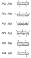
- a protection agent such as epoxy resin is first applied to surface 3 of the device of wafer 1 before mirror surface grinding and dicing as protection agent 2.
- the protection agent does not need to be epoxy resin. It has only to be a material that is not eroded in the etching process (Fig. 2(e)) that is done later. For example, heat curable resin, thermoplastic resin, etc. are fine.
- the purpose of applying the protection agent is that it prevents erosion of the device surface of the IC chip by the etching process (Fig. 2(e)).
- the protection agent is applied before mirror surface grinding and dicing and after the circuit installation. It is contemplated to apply the protection agent after mirror surface grinding.
- the time of the protection agent application is before dicing process, otherwise it is not limited especially.
- the mirror surface grinding process (Fig. 2(b)) is done from the side of the previous mirror surface 4 of the wafer.
- the thickness may be 0.76 - 0.25mm.
- the IC chip needs grinding until the thickness becomes 0.2mm or less.
- the IC chip stored in the IC card likewise with the IC card, is bent by force applied from the outside when carrying and using the IC card. Transformation arises and a stress occurs on the surface of the IC chip.
- the thickness of the IC chip is defined as T
- the Young's modulus of the IC chip is defined as E
- radius of curvature of the IC chip is defmed as R.
- the thickness of the IC chip is reduced, the bending stress of the IC chip is reduced for a bending transformation of an IC chip of the same radius of curvature. Therefore, as for the IC chip, it is desirable that it is ground as thin as possible. However, grinding flaws 6 arises in mirror surfaces 5 of wafer 1 at the time of mirror surfaces grinding.
- the IC card of which the thickness is 0.46mm or more.
- the IC chip of which the bending strength is high can be manufactured. Manufacturing of the IC card of high reliability is enabled.
- Dicing process (Fig. 2(c)) of the next ground IC chip is done. Dicing uses a blade of 20 ⁇ m thickness here. The protection agent also is cut with the wafer by dicing process (Fig. 2(c)). There is a fear of the occurrence of chipping 7 in the circumference part of the IC chip by dicing process (Fig. 2(c)). A chipping generation mechanism is shown in Fig. 6. When blade 10 cuts protection agents 2 and wafer 1, the part of wafer that is not cut destroys the part from which wafer was cut as starting point 15. This destruction is called chipping. It is thought that the vibration that is given to wafer 1 by the rotation of blade 10 is the cause of this.
- Fig. 5 shows the chipping that occurs in the IC chip by dicing.
- Chipping 7 comes to the circumference of the IC chip like a notch.
- the depth of chipping 7 is generally from 10 ⁇ m to more than 100 ⁇ m.
- Chipping 7 can reduce the bending strength of the IC chip.
- the method of slowing the transmission speed of the blade 10 in order to reduce generation of this chipping as much as possible has been considered. But this method would increase the time that is needed in dicing process.
- coming of the sharp notch of the chipping 7 tip part is removed in the back etching process (Fig. 2(e)).
- the chip after dicing consists like of Fig. 2(d). Grinding flaw 6 and chipping 7 arise in mirror surface 5 in IC chip 8 after dicing.
- Etching processing is done by chemical etching by the mixture liquid of fluoric acid, nitric acid and acetic acid.
- IC chip 8 the surface without device surface 3 (mirror surface 5 and side) protected by resisting is processed by this etching.
- the purpose of etching processing is not to remove all chipping 7 that occurs in mirror surface 5 of IC chip 8 and all grinding flaws 6.
- the purpose of etching processing is to remove sharp notches coming from the chipping tip part or the grinding flaw tip part that influence declination of the bending strength of the IC chip.
- the bending strength improvement of the IC chip has the advantage sufficiently in 10 ⁇ m or less. Even if the etching quantity is greatly taken, the problem of erosion of the part does not arise other than the mirror surface of the IC chip. If the etching quantity is increased, the advantage of the bending strength improvement of the chip also increases. After the etching process (Fig. 2(e)), protection agent removal (Fig. 2(f)) is done.
- the protection agent applied on device surface 3 of IC chip 9 is eliminated.
- the protection agent removal is chemically performed by dipping the IC chip in the protection agent removal liquid. While acetone was used as a protection agent removal liquid in this example, the protection agent removal liquid is not limited to this, the protection agent can be removed, and device surface 3 of IC chip 8 has only not be eroded.
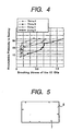
- Fig. 7 is the result that the bending strength of IC chip 9 of this example is measured.
- the bending strength of the IC chip is measured by a three point bending test.
- the result that the bending strength of the IC chip that does not eliminate the chipping that occurs in dicing is shown in Fig. 7.
- the bending strength of the IC chip of this example becomes 2 times or more the bending strength of the IC chip manufactured in the conventional method.
- the method of manufacturing the IC chip by this example provides IC chip that is less easily destroyed.
- the present invention provides an IC card and its manufacturing method of high reliability for an improved chip breakage to the IC chip.
Landscapes
- Engineering & Computer Science (AREA)
- Computer Hardware Design (AREA)
- Microelectronics & Electronic Packaging (AREA)
- Physics & Mathematics (AREA)
- General Physics & Mathematics (AREA)
- Theoretical Computer Science (AREA)
- Credit Cards Or The Like (AREA)
- Dicing (AREA)
Claims (10)
- IC-Karte, umfassend
wenigstens einen IC-Chip (9) und
Basisplatten (11), die weicher als der IC-Chip (9) sind, wobei die Basisplatten (11) geschichtet sind und die äußere Form der IC-Karte bilden, wobei der IC-Chip (9) innerhalb der IC-Karte angeordnet ist,
wobei der wenigstens eine IC-Chip umfaßt:wobei die Spiegeloberfläche (5) geätzt ist, wodurch scharfe Bereiche von in der Spiegeloberfläche (5) geformten Schleiffehlern (6) im wesentlichen beseitigt sind, undeine Geräteoberfläche (3), auf der eine Schaltung ausgebildet ist,eine Spiegeloberfläche (5), die auf der der Geräteoberfläche (3) gegenüberliegenden Seite angeordnet ist, undSeitenoberflächen, die im wesentlichen senkrecht zur Geräteoberfläche (3) sind, und
gekennzeichnet dadurch, daß die Seitenoberflächen ebenfalls geätzt sind, wodurch scharfe Bereiche von Ausplatzern (7), die in der Spiegeloberfläche (5) und den Seitenoberflächen am Umfangsrand der Spiegeloberfläche (5) gebildet sind, im wesentlichen beseitigt sind. - IC-Karte nach Anspruch 1, wobei der IC-Chip (9) aus Silizium hergestellt ist.
- IC-Karte nach Anspruch 1 oder 2, wobei der IC-Chip (9) 0,2 mm oder weniger dick ist.
- IC-Karte nach einem der vorhergehenden Ansprüche, wobei die Ätztiefe von der äußeren Form des IC-Chips (9) aus geringer ist als die Tiefe der Schleiffehler (6) und der Ausplatzer (7) von der äußeren Form des IC-Chips (4) aus bis zum unteren Ende der Schleiffehler (6) und der Ausplatzer (7).
- Verfahren zum Herstellen eines IC-Chips (9) zum Anordnen innerhalb einer IC-Karte, deren äußere Form durch geschichtete Basisplatten (11) gebildet ist, die weicher als der IC-Chip (9) sind, wobei das Verfahren die folgenden Schritte umfaßt:gekennzeichnet durch die folgenden Schritte:Ausbilden einer Schaltung auf einer Geräteoberfläche (3) eines Wafers (1),Anwenden eines Schutzmittels (2) auf die Geräteoberfläche (3) des Wafers (1), undDicen des Wafers (1), um einige IC-Chips (9) herzustellen,Ätzen des durch Dicen des Wafers (1) hergestellten IC-Chips (9), um sowohl eine Spiegeloberfläche (5) des IC-Chips (9), die auf der der Geräteoberfläche (3) gegenüberliegenden Seite angeordnet ist, als auch Seitenoberflächen des IC-Chips (9), die zur Geräteoberfläche (3) im wesentlichen senkrechte Oberflächen darstellen, zu ätzen, wodurch scharfe Bereiche von auf der Spiegeloberfläche (5) geformten Schleiffehlern (6) und scharfe Bereiche von in der Spiegeloberfläche (5) und den Seitenoberflächen am Umfangsrand der Spiegeloberfläche (5) geformten Ausplatzern (7) im wesentlichen beseitigt werden,Entfernen des Schutzmittels (2).
- Verfahren zum Herstellen eines IC-Chips nach Anspruch 5, wobei das Schutzmittel (2) auf den IC-Chip (9) vor dem Dicen des Wafers angewendet wird.
- Verfahren zum Herstellen eines IC-Chips nach Anspruch 5 oder 6, wobei der IC-Chip (9) durch chemisches Ätzen mit einer Mischflüssigkeit geätzt wird.
- Verfahren zum Herstellen eines IC-Chips nach Anspruch 7, wobei die Mischflüssigkeit Fluorsäure, Stickstoffsäure und Essigsäure umfaßt.
- Verfahren zum Herstellen eines (IC-Chips nach einem der Ansprüche 5 bis 8, wobei die Ätztiefe von der äußeren Form der IC-Karte (9) aus geringer ist als die Tiefe der Schleiffehler (6) und der Ausplatzer (7) von der äußeren Form des IC-Chips (9) aus bis zum unteren Ende der Schleiffehler (6) und der Ausplatzer.
- Verfahren zum Herstellen einer IC-Karte, umfassend die folgenden Schritte:Herstellen eines IC-Chips (9) mittels eines Verfahrens nach einem der vorhergehenden Ansprüche, undAnbringen des IC-Chips (9) innerhalb der geschichteten Basisplatten (11), die weicher als der IC-Chip (9) sind.
Applications Claiming Priority (2)
| Application Number | Priority Date | Filing Date | Title |
|---|---|---|---|
| JP26430798 | 1998-09-18 | ||
| JP26430798A JP2000099678A (ja) | 1998-09-18 | 1998-09-18 | Icカード及びその製造方法 |
Publications (3)
| Publication Number | Publication Date |
|---|---|
| EP0987652A2 EP0987652A2 (de) | 2000-03-22 |
| EP0987652A3 EP0987652A3 (de) | 2002-07-03 |
| EP0987652B1 true EP0987652B1 (de) | 2005-04-06 |
Family
ID=17401369
Family Applications (1)
| Application Number | Title | Priority Date | Filing Date |
|---|---|---|---|
| EP99307396A Expired - Lifetime EP0987652B1 (de) | 1998-09-18 | 1999-09-17 | IC-Karte und Herstellungsverfahren derselben |
Country Status (3)
| Country | Link |
|---|---|
| US (1) | US6554194B1 (de) |
| EP (1) | EP0987652B1 (de) |
| JP (1) | JP2000099678A (de) |
Families Citing this family (6)
| Publication number | Priority date | Publication date | Assignee | Title |
|---|---|---|---|---|
| JP2000099678A (ja) | 1998-09-18 | 2000-04-07 | Hitachi Ltd | Icカード及びその製造方法 |
| JP3883784B2 (ja) * | 2000-05-24 | 2007-02-21 | 三洋電機株式会社 | 板状体および半導体装置の製造方法 |
| JP3478281B2 (ja) * | 2001-06-07 | 2003-12-15 | ソニー株式会社 | Icカード |
| WO2004038793A1 (ja) * | 2002-10-24 | 2004-05-06 | Toray Engineering Company,Limited | 非接触idカード類及びその製造方法 |
| US20060140860A1 (en) * | 2004-12-08 | 2006-06-29 | Genstruct, Inc. | Computational knowledge model to discover molecular causes and treatment of diabetes mellitus |
| US7717326B2 (en) * | 2006-11-15 | 2010-05-18 | International Business Machines Corporation | Method and system for protecting data |
Family Cites Families (29)
| Publication number | Priority date | Publication date | Assignee | Title |
|---|---|---|---|---|
| US3888708A (en) * | 1972-02-17 | 1975-06-10 | Kensall D Wise | Method for forming regions of predetermined thickness in silicon |
| US3984620A (en) * | 1975-06-04 | 1976-10-05 | Raytheon Company | Integrated circuit chip test and assembly package |
| FR2527036A1 (fr) * | 1982-05-14 | 1983-11-18 | Radiotechnique Compelec | Procede pour connecter un semiconducteur a des elements d'un support, notamment d'une carte portative |
| DE3338597A1 (de) * | 1983-10-24 | 1985-05-02 | GAO Gesellschaft für Automation und Organisation mbH, 8000 München | Datentraeger mit integriertem schaltkreis und verfahren zur herstellung desselben |
| JPS60252992A (ja) * | 1984-05-30 | 1985-12-13 | Toshiba Corp | Icカ−ド |
| US4727246A (en) * | 1984-08-31 | 1988-02-23 | Casio Computer Co., Ltd. | IC card |
| JPS6182285A (ja) * | 1984-09-29 | 1986-04-25 | Toshiba Corp | Icカ−ド |
| JPS61123990A (ja) * | 1984-11-05 | 1986-06-11 | Casio Comput Co Ltd | Icカ−ド |
| US4845351A (en) * | 1985-09-30 | 1989-07-04 | Casio Computer Co., Ltd. | IC card |
| JPH0517270Y2 (de) * | 1986-07-03 | 1993-05-10 | ||
| DE3639630A1 (de) * | 1986-11-20 | 1988-06-01 | Gao Ges Automation Org | Datentraeger mit integriertem schaltkreis und verfahren zur herstellung desselben |
| JP2603952B2 (ja) | 1987-07-07 | 1997-04-23 | 株式会社東芝 | Icカード |
| JP2639153B2 (ja) * | 1990-01-26 | 1997-08-06 | 日本電気株式会社 | 半導体素子の製造方法 |
| JPH0462921A (ja) | 1990-06-29 | 1992-02-27 | Miyazaki Oki Electric Co Ltd | 半導体材料の裏面エッチング方法 |
| JPH06232255A (ja) | 1993-01-29 | 1994-08-19 | Disco Abrasive Syst Ltd | ウェーハのダイシング方法 |
| US5689136A (en) * | 1993-08-04 | 1997-11-18 | Hitachi, Ltd. | Semiconductor device and fabrication method |
| US5326428A (en) * | 1993-09-03 | 1994-07-05 | Micron Semiconductor, Inc. | Method for testing semiconductor circuitry for operability and method of forming apparatus for testing semiconductor circuitry for operability |
| US5481102A (en) * | 1994-03-31 | 1996-01-02 | Hazelrigg, Jr.; George A. | Micromechanical/microelectromechanical identification devices and methods of fabrication and encoding thereof |
| US5480842A (en) * | 1994-04-11 | 1996-01-02 | At&T Corp. | Method for fabricating thin, strong, and flexible die for smart cards |
| JP3222346B2 (ja) | 1995-03-08 | 2001-10-29 | 沖電気工業株式会社 | 発光素子アレイプリンタの光書き込み装置 |
| US5733814A (en) * | 1995-04-03 | 1998-03-31 | Aptek Industries, Inc. | Flexible electronic card and method |
| JPH08310172A (ja) * | 1995-05-23 | 1996-11-26 | Hitachi Ltd | 半導体装置 |
| FR2734983B1 (fr) * | 1995-05-29 | 1997-07-04 | Sgs Thomson Microelectronics | Utilisation d'un micromodule comme boitier de montage en surface et procede correspondant |
| JPH09270396A (ja) * | 1996-03-29 | 1997-10-14 | Komatsu Electron Metals Co Ltd | 半導体ウェハの製法 |
| US5786988A (en) * | 1996-07-02 | 1998-07-28 | Sandisk Corporation | Integrated circuit chips made bendable by forming indentations in their back surfaces flexible packages thereof and methods of manufacture |
| JP2000099678A (ja) | 1998-09-18 | 2000-04-07 | Hitachi Ltd | Icカード及びその製造方法 |
| JP3720599B2 (ja) * | 1998-10-07 | 2005-11-30 | 日本電信電話株式会社 | 半導体装置 |
| JP3447602B2 (ja) * | 1999-02-05 | 2003-09-16 | シャープ株式会社 | 半導体装置の製造方法 |
| JP2001156028A (ja) * | 1999-11-30 | 2001-06-08 | Lintec Corp | 半導体装置の製造方法 |
-
1998
- 1998-09-18 JP JP26430798A patent/JP2000099678A/ja active Pending
-
1999
- 1999-09-16 US US09/391,089 patent/US6554194B1/en not_active Expired - Fee Related
- 1999-09-17 EP EP99307396A patent/EP0987652B1/de not_active Expired - Lifetime
Also Published As
| Publication number | Publication date |
|---|---|
| EP0987652A2 (de) | 2000-03-22 |
| US6554194B1 (en) | 2003-04-29 |
| JP2000099678A (ja) | 2000-04-07 |
| EP0987652A3 (de) | 2002-07-03 |
Similar Documents
| Publication | Publication Date | Title |
|---|---|---|
| US8288842B2 (en) | Method for dicing semiconductor wafers | |
| KR100542850B1 (ko) | 반도체 장치의 제조 방법 | |
| US7638858B2 (en) | Semiconductor device and manufacturing method thereof | |
| US6075280A (en) | Precision breaking of semiconductor wafer into chips by applying an etch process | |
| EP1676310B1 (de) | Verfahren zur herstellung und zusammenstellung von substraten | |
| KR100588412B1 (ko) | 반도체 웨이퍼 분할방법 | |
| EP0676717B1 (de) | Flacher, widerstandsfähiger und flexibler Träger für IC-Karten | |
| KR102250130B1 (ko) | 반도체 소자의 제조 방법 | |
| US6933211B2 (en) | Semiconductor device whose semiconductor chip has chamfered backside surface edges and method of manufacturing the same | |
| WO2003036712A1 (en) | Method and apparatus for dicing a semiconductor wafer | |
| US6303471B1 (en) | Method of manufacturing semiconductor device having reinforcing member and method of manufacturing IC card using the device | |
| EP0987652B1 (de) | IC-Karte und Herstellungsverfahren derselben | |
| US20080029877A1 (en) | Method for separating package of wlp | |
| EP0850737A2 (de) | Mehrstufen-Verfahren zur Herstellung von Halbleiterscheiben | |
| KR100554994B1 (ko) | 반도체 장치의 제조 방법 | |
| US6174789B1 (en) | Method of dividing a compound semiconductor wafer into pellets by utilizing extremely narrow scribe regions | |
| JP2002319554A (ja) | ウェーハ分割方法およびウェーハ分割装置 | |
| JP2000040677A (ja) | 半導体素子の製造方法 | |
| JP5418160B2 (ja) | Icチップの製造方法 | |
| US6944370B2 (en) | Method of processing a semiconductor wafer | |
| JP2000011129A (ja) | Icカードおよびその製造方法 | |
| JP2003124147A (ja) | 半導体装置の製造方法 | |
| JPH04223356A (ja) | 半導体装置の製造方法 | |
| JP2001219386A (ja) | レーザマーク付き半導体ウエーハ製造方法 | |
| JP2007266043A (ja) | 化合物半導体ウェハ |
Legal Events
| Date | Code | Title | Description |
|---|---|---|---|
| PUAI | Public reference made under article 153(3) epc to a published international application that has entered the european phase |
Free format text: ORIGINAL CODE: 0009012 |
|
| 17P | Request for examination filed |
Effective date: 19990924 |
|
| AK | Designated contracting states |
Kind code of ref document: A2 Designated state(s): AT BE CH CY DE DK ES FI FR GB GR IE IT LI LU MC NL PT SE |
|
| AX | Request for extension of the european patent |
Free format text: AL;LT;LV;MK;RO;SI |
|
| PUAL | Search report despatched |
Free format text: ORIGINAL CODE: 0009013 |
|
| AK | Designated contracting states |
Kind code of ref document: A3 Designated state(s): AT BE CH CY DE DK ES FI FR GB GR IE IT LI LU MC NL PT SE |
|
| AX | Request for extension of the european patent |
Free format text: AL;LT;LV;MK;RO;SI |
|
| AKX | Designation fees paid |
Designated state(s): FR GB |
|
| REG | Reference to a national code |
Ref country code: DE Ref legal event code: 8566 |
|
| 17Q | First examination report despatched |
Effective date: 20031208 |
|
| GRAP | Despatch of communication of intention to grant a patent |
Free format text: ORIGINAL CODE: EPIDOSNIGR1 |
|
| GRAS | Grant fee paid |
Free format text: ORIGINAL CODE: EPIDOSNIGR3 |
|
| GRAA | (expected) grant |
Free format text: ORIGINAL CODE: 0009210 |
|
| AK | Designated contracting states |
Kind code of ref document: B1 Designated state(s): FR GB |
|
| REG | Reference to a national code |
Ref country code: GB Ref legal event code: FG4D |
|
| REG | Reference to a national code |
Ref country code: IE Ref legal event code: FG4D |
|
| PG25 | Lapsed in a contracting state [announced via postgrant information from national office to epo] |
Ref country code: GB Free format text: LAPSE BECAUSE OF NON-PAYMENT OF DUE FEES Effective date: 20050917 |
|
| PLBE | No opposition filed within time limit |
Free format text: ORIGINAL CODE: 0009261 |
|
| STAA | Information on the status of an ep patent application or granted ep patent |
Free format text: STATUS: NO OPPOSITION FILED WITHIN TIME LIMIT |
|
| 26N | No opposition filed |
Effective date: 20060110 |
|
| GBPC | Gb: european patent ceased through non-payment of renewal fee |
Effective date: 20050917 |
|
| EN | Fr: translation not filed | ||
| PG25 | Lapsed in a contracting state [announced via postgrant information from national office to epo] |
Ref country code: FR Free format text: LAPSE BECAUSE OF NON-PAYMENT OF DUE FEES Effective date: 20050930 |
|
| PG25 | Lapsed in a contracting state [announced via postgrant information from national office to epo] |
Ref country code: FR Free format text: LAPSE BECAUSE OF NON-PAYMENT OF DUE FEES Effective date: 20050406 |