EP0985534A1 - Procede de formation d'ajutage pour injecteurs et procede de fabrication d'une tete a jet d'encre - Google Patents
Procede de formation d'ajutage pour injecteurs et procede de fabrication d'une tete a jet d'encre Download PDFInfo
- Publication number
- EP0985534A1 EP0985534A1 EP98919579A EP98919579A EP0985534A1 EP 0985534 A1 EP0985534 A1 EP 0985534A1 EP 98919579 A EP98919579 A EP 98919579A EP 98919579 A EP98919579 A EP 98919579A EP 0985534 A1 EP0985534 A1 EP 0985534A1
- Authority
- EP
- European Patent Office
- Prior art keywords
- etching
- nozzle
- silicon
- forming
- substrate
- Prior art date
- Legal status (The legal status is an assumption and is not a legal conclusion. Google has not performed a legal analysis and makes no representation as to the accuracy of the status listed.)
- Withdrawn
Links
- 238000000034 method Methods 0.000 title claims description 90
- 238000004519 manufacturing process Methods 0.000 title claims description 46
- 239000000758 substrate Substances 0.000 claims abstract description 85
- XUIMIQQOPSSXEZ-UHFFFAOYSA-N Silicon Chemical compound [Si] XUIMIQQOPSSXEZ-UHFFFAOYSA-N 0.000 claims abstract description 82
- 229910052710 silicon Inorganic materials 0.000 claims abstract description 82
- 239000010703 silicon Substances 0.000 claims abstract description 82
- 238000005530 etching Methods 0.000 claims abstract description 72
- 238000001312 dry etching Methods 0.000 claims abstract description 38
- 238000000059 patterning Methods 0.000 claims abstract description 20
- VYPSYNLAJGMNEJ-UHFFFAOYSA-N Silicium dioxide Chemical compound O=[Si]=O VYPSYNLAJGMNEJ-UHFFFAOYSA-N 0.000 claims description 68
- 238000001039 wet etching Methods 0.000 claims description 5
- 238000000347 anisotropic wet etching Methods 0.000 claims description 3
- 230000000149 penetrating effect Effects 0.000 claims description 3
- SFZCNBIFKDRMGX-UHFFFAOYSA-N sulfur hexafluoride Chemical compound FS(F)(F)(F)(F)F SFZCNBIFKDRMGX-UHFFFAOYSA-N 0.000 claims description 3
- 229960000909 sulfur hexafluoride Drugs 0.000 claims description 3
- TXEYQDLBPFQVAA-UHFFFAOYSA-N tetrafluoromethane Chemical compound FC(F)(F)F TXEYQDLBPFQVAA-UHFFFAOYSA-N 0.000 claims description 3
- 238000002347 injection Methods 0.000 claims description 2
- 239000007924 injection Substances 0.000 claims description 2
- 229910052814 silicon oxide Inorganic materials 0.000 claims 2
- 229910021421 monocrystalline silicon Inorganic materials 0.000 abstract description 3
- 229910052681 coesite Inorganic materials 0.000 description 33
- 229910052906 cristobalite Inorganic materials 0.000 description 33
- 239000000377 silicon dioxide Substances 0.000 description 33
- 229910052682 stishovite Inorganic materials 0.000 description 33
- 229910052905 tridymite Inorganic materials 0.000 description 33
- KRHYYFGTRYWZRS-UHFFFAOYSA-N Fluorane Chemical compound F KRHYYFGTRYWZRS-UHFFFAOYSA-N 0.000 description 8
- 239000007789 gas Substances 0.000 description 8
- 239000007864 aqueous solution Substances 0.000 description 5
- 239000011521 glass Substances 0.000 description 5
- DDFHBQSCUXNBSA-UHFFFAOYSA-N 5-(5-carboxythiophen-2-yl)thiophene-2-carboxylic acid Chemical compound S1C(C(=O)O)=CC=C1C1=CC=C(C(O)=O)S1 DDFHBQSCUXNBSA-UHFFFAOYSA-N 0.000 description 3
- KWYUFKZDYYNOTN-UHFFFAOYSA-M Potassium hydroxide Chemical compound [OH-].[K+] KWYUFKZDYYNOTN-UHFFFAOYSA-M 0.000 description 3
- 229910018503 SF6 Inorganic materials 0.000 description 3
- 239000007788 liquid Substances 0.000 description 3
- 230000015572 biosynthetic process Effects 0.000 description 2
- 238000006243 chemical reaction Methods 0.000 description 2
- WRQGPGZATPOHHX-UHFFFAOYSA-N ethyl 2-oxohexanoate Chemical compound CCCCC(=O)C(=O)OCC WRQGPGZATPOHHX-UHFFFAOYSA-N 0.000 description 2
- 238000001020 plasma etching Methods 0.000 description 2
- 238000005507 spraying Methods 0.000 description 2
- BSYNRYMUTXBXSQ-UHFFFAOYSA-N Aspirin Chemical compound CC(=O)OC1=CC=CC=C1C(O)=O BSYNRYMUTXBXSQ-UHFFFAOYSA-N 0.000 description 1
- LDDQLRUQCUTJBB-UHFFFAOYSA-N ammonium fluoride Chemical compound [NH4+].[F-] LDDQLRUQCUTJBB-UHFFFAOYSA-N 0.000 description 1
- 238000007796 conventional method Methods 0.000 description 1
- 239000013078 crystal Substances 0.000 description 1
- 230000006866 deterioration Effects 0.000 description 1
- 238000007598 dipping method Methods 0.000 description 1
- 239000000446 fuel Substances 0.000 description 1
- 230000006698 induction Effects 0.000 description 1
- 230000000873 masking effect Effects 0.000 description 1
- 230000002093 peripheral effect Effects 0.000 description 1
- 238000000206 photolithography Methods 0.000 description 1
- 230000001105 regulatory effect Effects 0.000 description 1
- 230000001846 repelling effect Effects 0.000 description 1
- 239000011347 resin Substances 0.000 description 1
- 229920005989 resin Polymers 0.000 description 1
- XLYOFNOQVPJJNP-UHFFFAOYSA-N water Substances O XLYOFNOQVPJJNP-UHFFFAOYSA-N 0.000 description 1
Images


Classifications
-
- B—PERFORMING OPERATIONS; TRANSPORTING
- B41—PRINTING; LINING MACHINES; TYPEWRITERS; STAMPS
- B41J—TYPEWRITERS; SELECTIVE PRINTING MECHANISMS, i.e. MECHANISMS PRINTING OTHERWISE THAN FROM A FORME; CORRECTION OF TYPOGRAPHICAL ERRORS
- B41J2/00—Typewriters or selective printing mechanisms characterised by the printing or marking process for which they are designed
- B41J2/005—Typewriters or selective printing mechanisms characterised by the printing or marking process for which they are designed characterised by bringing liquid or particles selectively into contact with a printing material
- B41J2/01—Ink jet
- B41J2/135—Nozzles
- B41J2/16—Production of nozzles
- B41J2/1621—Manufacturing processes
- B41J2/1626—Manufacturing processes etching
- B41J2/1629—Manufacturing processes etching wet etching
-
- B—PERFORMING OPERATIONS; TRANSPORTING
- B41—PRINTING; LINING MACHINES; TYPEWRITERS; STAMPS
- B41J—TYPEWRITERS; SELECTIVE PRINTING MECHANISMS, i.e. MECHANISMS PRINTING OTHERWISE THAN FROM A FORME; CORRECTION OF TYPOGRAPHICAL ERRORS
- B41J2/00—Typewriters or selective printing mechanisms characterised by the printing or marking process for which they are designed
- B41J2/005—Typewriters or selective printing mechanisms characterised by the printing or marking process for which they are designed characterised by bringing liquid or particles selectively into contact with a printing material
- B41J2/01—Ink jet
- B41J2/135—Nozzles
- B41J2/16—Production of nozzles
- B41J2/162—Manufacturing of the nozzle plates
-
- B—PERFORMING OPERATIONS; TRANSPORTING
- B41—PRINTING; LINING MACHINES; TYPEWRITERS; STAMPS
- B41J—TYPEWRITERS; SELECTIVE PRINTING MECHANISMS, i.e. MECHANISMS PRINTING OTHERWISE THAN FROM A FORME; CORRECTION OF TYPOGRAPHICAL ERRORS
- B41J2/00—Typewriters or selective printing mechanisms characterised by the printing or marking process for which they are designed
- B41J2/005—Typewriters or selective printing mechanisms characterised by the printing or marking process for which they are designed characterised by bringing liquid or particles selectively into contact with a printing material
- B41J2/01—Ink jet
- B41J2/135—Nozzles
- B41J2/16—Production of nozzles
- B41J2/1621—Manufacturing processes
- B41J2/1626—Manufacturing processes etching
- B41J2/1628—Manufacturing processes etching dry etching
-
- B—PERFORMING OPERATIONS; TRANSPORTING
- B41—PRINTING; LINING MACHINES; TYPEWRITERS; STAMPS
- B41J—TYPEWRITERS; SELECTIVE PRINTING MECHANISMS, i.e. MECHANISMS PRINTING OTHERWISE THAN FROM A FORME; CORRECTION OF TYPOGRAPHICAL ERRORS
- B41J2/00—Typewriters or selective printing mechanisms characterised by the printing or marking process for which they are designed
- B41J2/005—Typewriters or selective printing mechanisms characterised by the printing or marking process for which they are designed characterised by bringing liquid or particles selectively into contact with a printing material
- B41J2/01—Ink jet
- B41J2/135—Nozzles
- B41J2/16—Production of nozzles
- B41J2/1621—Manufacturing processes
- B41J2/1635—Manufacturing processes dividing the wafer into individual chips
-
- B—PERFORMING OPERATIONS; TRANSPORTING
- B41—PRINTING; LINING MACHINES; TYPEWRITERS; STAMPS
- B41J—TYPEWRITERS; SELECTIVE PRINTING MECHANISMS, i.e. MECHANISMS PRINTING OTHERWISE THAN FROM A FORME; CORRECTION OF TYPOGRAPHICAL ERRORS
- B41J2/00—Typewriters or selective printing mechanisms characterised by the printing or marking process for which they are designed
- B41J2/005—Typewriters or selective printing mechanisms characterised by the printing or marking process for which they are designed characterised by bringing liquid or particles selectively into contact with a printing material
- B41J2/01—Ink jet
- B41J2/015—Ink jet characterised by the jet generation process
- B41J2/04—Ink jet characterised by the jet generation process generating single droplets or particles on demand
- B41J2002/043—Electrostatic transducer
-
- B—PERFORMING OPERATIONS; TRANSPORTING
- B41—PRINTING; LINING MACHINES; TYPEWRITERS; STAMPS
- B41J—TYPEWRITERS; SELECTIVE PRINTING MECHANISMS, i.e. MECHANISMS PRINTING OTHERWISE THAN FROM A FORME; CORRECTION OF TYPOGRAPHICAL ERRORS
- B41J2/00—Typewriters or selective printing mechanisms characterised by the printing or marking process for which they are designed
- B41J2/005—Typewriters or selective printing mechanisms characterised by the printing or marking process for which they are designed characterised by bringing liquid or particles selectively into contact with a printing material
- B41J2/01—Ink jet
- B41J2/135—Nozzles
- B41J2/14—Structure thereof only for on-demand ink jet heads
- B41J2002/14387—Front shooter
-
- B—PERFORMING OPERATIONS; TRANSPORTING
- B41—PRINTING; LINING MACHINES; TYPEWRITERS; STAMPS
- B41J—TYPEWRITERS; SELECTIVE PRINTING MECHANISMS, i.e. MECHANISMS PRINTING OTHERWISE THAN FROM A FORME; CORRECTION OF TYPOGRAPHICAL ERRORS
- B41J2/00—Typewriters or selective printing mechanisms characterised by the printing or marking process for which they are designed
- B41J2/005—Typewriters or selective printing mechanisms characterised by the printing or marking process for which they are designed characterised by bringing liquid or particles selectively into contact with a printing material
- B41J2/01—Ink jet
- B41J2/135—Nozzles
- B41J2/14—Structure thereof only for on-demand ink jet heads
- B41J2002/14411—Groove in the nozzle plate
Definitions
- the present invention relates to a method of forming a nozzle for an ejection device for ejecting or spraying a liquid or gas. More particularly, the present invention relates to a method of forming a nozzle having a cross-section which is made smaller stepwise toward the ejecting front end thereof by etching a silicon monocrystalline substrate. Furthermore, the present invention relates to a method of forming a nozzle plate which is preferable for an inkjet head for ejecting ink droplets.
- the inkjet head of an inkjet printer generally comprises a plurality of nozzles for ejecting ink droplets therefrom and an ink supply passage communicating with the nozzles.
- a nozzle having such a cross-sectional shape that a thin nozzle hole portion is formed on the front end side thereof and a nozzle hole portion expanding in a conical shape or a pyramidal shape is formed at the rear end side thereof in order to improve the ink ejection characteristics of the respective nozzles of an inkjet head.
- the direction in which the nozzle ejects ink droplets in response to ink pressure from an ink cavity side can be aligned in the axial direction of the nozzles, as compared with the case of a cylindrical nozzle.
- Stable ink ejection characteristics can be obtained thereby. That is, since variations in the trajectories of ink droplets can be eliminated, they are prevented from flying in differing directions, whereby variations in the amount of ink in each droplet can be suppressed.
- Japanese Unexamined Patent Publication No. 5-50601 discloses a method of manufacturing an electrostatic-drive type inkjet head in which a nozzle and an ink supply passage are formed with pinpoint accuracy by applying photolithography and wet-type-crystal-anisotropic-etching to a silicon monocrystalline substrate.
- the inkjet head disclosed in this publication employs a structure in which nozzles, reservoirs, ink supply passages such as cavities and the like, and diaphragms are formed in a silicon monocrystalline substrate bonded to a glass electrode substrate, on which electrodes for deflecting the diaphragms by electrostatic force are formed.
- this structure allows a manufacturing method to be employed in which, after the patterns (nozzles, ink supply passages, electrodes) of respective inkjet heads are formed in or on the respective substrates, the substrates are bonded to each other and the thus-bonded substrates are cut and separated into respective inkjet heads (the so-called method of making multiple inkjet heads from a single substrate), whereby the inkjet heads can be manufactured at low cost.
- the so-called method of making multiple inkjet heads from a single substrate is disclosed in Japanese Unexamined Patent Publication No. 9-300630, filed by the applicant.
- this publication proposes a method of bonding together a plurality of cover substrates and a flow passage substrate in a row state so that so that the cover substrates are arranged on the flow passage substrate in a row, and terminals formed at a lower substrate to supply a signal or power are exposed.
- nozzles are formed in a cover substrate for covering an ink supply passage and the cover substrate itself is used as a nozzle plate, it is preferable for accuracy that after a single nozzle plate is bonded to a flow passage substrate, the combined substrates be separated to respective inkjet heads, as compared with the method disclosed in Japanese Unexamined Patent Publication No. 9-300630.
- a through-hole for exposing terminals formed on the lower substrate must be formed, in addition to the nozzles, on the nozzle plate as the uppermost substrate of these three substrates.
- Etching is carried out at a relatively low rate in a process for forming nozzle holes because pinpoint processing accuracy is required in the process.
- etching is carried out at a relatively high rate in a process for forming the through-hole where a reduction in etching time takes priority over processing accuracy because accuracy requirements for the through-hole are not as stringent as that for the nozzle holes.
- the process for forming the nozzle holes and the process for forming the through-hole, the etching conditions of which are different from each other have ordinarily been performed independently from each other. That is, after the through-hole is formed by etching, the nozzle holes are etched; or after the nozzle holes are formed by etching, the through-hole etched.
- the present invention employs a dry-etching method by ICP (induction coupled plasma) discharge as an anisotropic dry-etching method to form a nozzle having a cross-section made smaller stepwise toward the front end thereof by applying etching to a silicon monocrystalline substrate.
- ICP induction coupled plasma
- an oxidized silicon film for example, is formed as a resist film on a surface of the silicon monocrystalline substrate.
- a first opening pattern is formed by removing the resist film at a portion corresponding to the rear end of the nozzle and a second opening pattern which is smaller than the first pattern is formed by removing the resist film at a portion corresponding to the front end of the nozzle.
- dry-etching is applied by plasma discharge to the exposed portions of the surface of the silicon monocrystalline substrate exposed by the first and second opening patterns.
- a gas for etching silicon by conversion to a plasma by plasma discharge and a gas for suppressing the etching of silicon by conversion to a plasma by plasma discharge are alternately charged into a processing vessel in which the silicon substrate is disposed.
- a nozzle is formed having a cross-section which coincides with the shapes of the respective opening patterns and is made smaller stepwise from the rear end thereof toward the front end thereof.
- a nozzle whose cross-section is made smaller stepwise from the rear end thereof toward the front end thereof can be formed by performing dry-etching only from one side of the silicon substrate, whereby the manufacturing process can be further simplified.
- the opening pattern which corresponds to the portion of the nozzle at the rear end thereof, is formed at the resist film by half-etching the resist film (first patterning process).
- an opening pattern which corresponds to the portion of the nozzle at the front end thereof is formed as the exposed portion of the surface of the silicon monocrystalline substrate by full-etching a portion of the half-etched region of the resist film at which the above opening pattern is formed (second patterning process)-
- a first groove having a predetermined depth is formed by applying dry-etching to the exposed portion of the silicon monocrystalline substrate by plasma discharge (first dry-etching process).
- a second groove having a predetermined depth, while the first groove remains on the bottom thereof, is formed by applying dry-etching to the silicon monocrystalline substrate by plasma discharge (second dry-etching process).
- the etching of the surface of the silicon monocrystalline substrate is conducted in a state in which the first groove which was formed first by the etching remains as it is, and the second groove is formed.
- the depth of the portion of the first groove can be set to a size which coincides with the nozzle at the front end thereof having a small cross-section and the depth of the portion of the second groove can be set to a size which coincides with the nozzle at the rear end thereof having a large cross-section.
- a master pattern need not be repeatedly formed on the surface of the silicon monocrystalline substrate. Furthermore, a master pattern need not be formed along the surface of the silicon monocrystalline substrate in the stepwise state after a recess is formed at the silicon monocrystalline substrate.
- the nozzle having the stepwise-cross-section can be effectively and simply formed.
- the present invention employs a method arranged such that a first fine groove acting as the nozzle is formed up to a predetermined depth and a second groove acting as a part of a through-hole, which exposes a terminal disposed on a substrate to be bonded to the lower side of a substrate serving as a nozzle plate, are formed from a surface of the substrate serving as the nozzle plate by etching. Thereafter, a third groove, larger than the first groove, is formed from the other surface of the upper substrate by etching, and the nozzle and the through-hole are simultaneously formed by penetrating the first groove and the second groove.
- the through-hole can be formed simultaneously with the nozzle without lowering processing accuracy.
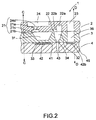
- Fig. 1 is an exploded perspective view of an inkjet head to which a method of the present invention can be applied
- Fig. 2 shows a schematic cross-section of the inkjet head in Fig. 1.
- the inkjet head 1 of the example is an electrostatic-drive type inkjet head similar to the inkjet head disclosed in Japanese Unexamined Patent Publication No. 5-50601, filed by the applicant.
- the inkjet head 1 is arranged by similarly bonding together a nozzle plate 2 (upper substrate) composed of a silicon monocrystalline substrate, a cavity plate 3 (first lower substrate) composed of a silicon monocrystalline substrate, and a glass substrate 4 (second lower substrate).
- a plurality of ink cavities 31 and a common ink reservoir 32 for supplying ink to the respective ink cavities 31 are formed on the cavity plate 3.
- a plurality of nozzles 21 communicating with the respective ink cavities 31 and ink supply ports 22 for communicating the respective ink cavities 31 with the common ink reservoir 32 are formed in the nozzle plate 2.
- Each ink supply port 22 has a cross-sectional-shape such that a deep groove portion 22a is formed at one end thereof and a shallow groove portion 22b is farmed at the other end thereof.
- Recesses 41 are formed on the glass substrate 4, which is bonded to the back surface of the cavity plate 3, at the portions thereof confronting diaphragms 33 which define the bottoms of the ink cavities 31.
- Individual electrodes 42 are formed on the bottoms of the recesses in confrontation with the diaphragms 33.
- the individual electrodes 42 are connected to individual terminals 42b disposed in recesses 45 through leads 42a disposed in grooves 44.
- a through-hole 36 is formed at the cavity plate 3 so that the individual terminals 42b are exposed when the cavity plate 3 is bonded to the glass substrate 4.
- a common terminal 35 is disposed in the vicinity of the through-hole 36 to supply electrical charge to the diaphragms 33.
- a through-hole 23 is also formed at the nozzle plate 2 to expose the individual terminals 42b and the common terminal 35 when nozzle plate 2 is bonded to the lower substrate. After the bonded substrates are divided into the individual inkjet heads, an FPC (not shown) is connected to these individual terminals 42b and 35.
- an ink supply hole 34 is formed at the bottom of the ink reservoir 32 and communicates with an ink supply passage 43 formed through the glass substrate 4. Ink can be supplied from an external ink supply source to the ink reservoir 32 through the ink supply passage 43 and the ink supply hole 34.
- the diaphragms 33 formed at the cavity plate 3 and regulating the bottoms of the respective ink cavities 31 act as a common electrode.
- the diaphragms 33 confronting the individual electrodes 42 to which the voltage is applied are deflected by electrostatic force, whereby the volumes of the cavities 31 are changed and ink droplets are ejected from the nozzles 21.
- the nozzle 21 is a nozzle having a stepwise cross-section. That is, a nozzle portion 21a of a small circular cross-section (small cross-section portion) is formed on the front side of the nozzle 21 as seen in an ink droplet ejecting direction and a nozzle portion 21b of a large circular cross-section (large cross-section portion) is formed on the rear side thereof, as seen in same direction. Furthermore, the boundary portion therebetween is arranged as an annular stepped surface 21c. Therefore, the cross-sectional shape of the nozzle 21 is made smaller stepwise toward the front end thereof when taken along the axial line thereof. Furthermore, the opening 21d of the nozzle 21 at the front end thereof is opened to the bottom of a recess 24 formed at the opposite surface of the nozzle plate 2.
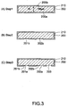
- Fig. 3 - Fig. 6 show an example of a process for manufacturing the nozzle plate 2. A procedure for manufacturing the nozzle plate 2 will be described with reference to these figures.
- Step 1 first thermally-oxidized-film forming process
- a silicon wafer 200 having a thickness of 180 microns is prepared and thermally oxidized, and an SiO 2 film 210 having a thickness of at least 1.2 microns is formed on the surface thereof as a resist film.
- Step 2 first patterning process of the SiO 2 film
- the SiO 2 film 210 covering the surface 200a of the silicon wafer 200 is half-etched and a pattern 201b and a pattern 202b are formed so as to form the large cross-section nozzle portion 21b of the nozzle 21 and the shallow groove portion 22b of the ink supply port 22.
- the etching depth can be set to, for example, 0.5 micron.
- Step 3 second patterning process of the SiO 2 film
- patterns 201a and 202a for forming the small cross-section nozzle portion 21a of the nozzle 21 and the deep groove portion 22a of the ink supply port 22 are formed at the portions of the patterns 201b and 202b as the half-etched regions of the SiO 2 film 210. That is, these half-etched regions are fully etched to thereby form the patterns 201a and 202a where the surface of the silicon wafer is exposed.
- a pattern 203 for forming the electrode through-hole 23 is also formed by full-etching the SiO 2 film 210 together with the above patterns.
- Ammonium fluoride similar to that used above, can also be used as an etchant at this time.
- a resist film of a light-sensitive resin is used as resist film for partially etching the SiO 2 film.
- the resist film is half-solidified when it is coated and then heated, and then it is completely solidified when it is further heated after it is exposed and developed. Thereafter, the SiO 2 film is etched as described above, whereby the resist film for etching the silicon is formed.
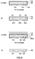
- Step 4 first dry-etching process
- anisotropic-dry-etching is applied to the silicon wafer 200 by plasma discharge as shown in Fig. 4(A).
- the surface of the silicon wafer 200 is etched perpendicularly to the substrate surface in shapes corresponding to the patterns 201b, 202b, and 203 formed at step 3, whereby grooves 221, 222, and 223, having the same depth, are formed, respectively.
- a carbon fluoride (CF) gas and sulfur hexafluoride (SF 6 ) can be alternately used as an etching gas.
- the CF gas is used to protect the sides of the grooves so that the etching does not advance thereto and the SF 6 is used to promote the etching in the vertical direction of the silicon wafer.
- the SiO 2 film 210 is removed in a thickness of 0.7 micron by etching with a hydrofluoric acid aqueous solution.
- the portions of the patterns 201b and 202b formed at step 2 are completely removed as shown in Fig. 4(B) so that the surface of the silicon wafer 200 is exposed.
- Step 5 second dry-etching process
- a nozzle groove 231 having a cross-sectional shape corresponding to the stepwise nozzle 21 and a groove 232 having a cross-sectional shape corresponding to the ink supply port 22 are formed.
- a groove 233 having a depth half that of the electrode disposing through-hole 23 is also formed.
- Step 6 second thermally-oxidized-film forming process
- the surface of the silicon wafer 200 is again thermally oxidized, thereby forming an SiO 2 film 240 as a resist film. It is sufficient to set the thickness of the SiO 2 film 240 to 1.2 microns in this case too.
- Step 7 third patterning process of the SiO 2 film
- the portion of the SiO 2 film 240 covering the surface of the silicon wafer 200 opposite to that processed before is etched as shown in Fig. 5(B) to thereby form a pattern 204 corresponding to the recess 24 where the nozzle 21 is opened and a pattern 203A corresponding to the through-hole 23.
- the etchant used at step 2 can be also used at this time.
- Step 8 wet-etching process
- anisotropic wet-etching is performed on the exposed portion of the silicon wafer 200 by dipping it into an etchant to form a groove 244 corresponding to the recess 24. Furthermore, a groove 233A corresponding to the through-hole 23 is formed.
- the etchant used at this time is a potassium hydroxide aqueous solution having a concentration of 2 wt% and a liquid temperature of 80°C.
- the etching depth is set to, for example, 110 microns.
- the SiO 2 film 240 is completely removed with a hydrofluoric acid aqueous solution, as shown in Fig. 5(D), so that the grooves 231 and 244 and the grooves 233 and 233A become connected, respectively.
- the silicon wafer is again thermally oxidized and an SiO 2 film is formed in order to secure the ink resistant property of the silicon wafer and the intimate contact property of a nozzle surface achieved by water repelling processing.
- the nozzle plate 2 can be obtained by the above procedure.
- etching is conducted on one surface side of the silicon wafer 200 for forming the nozzle plate 2 so that the fine groove 231 for the nozzle 21, and the groove 223 for the electrode wiring through-hole 23, are formed. Furthermore, the grooves 244 and 233A, which are larger than the groove of the nozzle 21, are formed from the other surface side of the silicon wafer 200 so that the groove 244 connects to the nozzle groove 231 to thereby form the nozzle 21, and the groove 233A connects to the groove 233 to thereby obtain the through-hole 23 at the same time.
- Fig. 7 - Fig. 10 show the manufacturing process of the nozzle plate 2 of another embodiment of the present invention.
- the manufacturing procedure of the nozzle plate 2 will be described with reference to these figures. In the following description, the description of the points overlapping with the above embodiment will be omitted.
- a first thermally-oxidized-film forming process is carried out in step 1 and a first patterning process for an SiO 2 film is carried out in step 2 in manners similar to those in the above embodiment.
- a second patterning process for the SiO 2 film is carried out in step 3 thereafter in a manner similar to that in the above embodiment.
- a pattern 303 for forming an electrode through-hole 23 is formed in the SiO 2 film 310 by full-etching it into a ring groove shape so that the contour of the outer periphery of the through-hole 23 is drawn.
- ammonium fluoride similar to that above, can be used as an etchant at this time.
- anisotropic-dry-etching is applied to the silicon wafer 300 by plasma discharge, for example, by ICP discharge as shown in Fig. 8(A) in manner similar to the above embodiment.
- step 4 one surface side of the silicon wafer 300 is vertically etched in the shapes corresponding to patterns 301b, 302b, and 303 formed in step 3, whereby grooves 321, 322, and 323 having the same depth are formed, respectively.
- the SiO 2 film 310 is completely removed at the portions of the patterns 301b and 302b with a hydrofluoric acid aqueous solution and anisotropic-dry-etching is carried out again by plasma discharge, for example, by ICP discharge as shown in Fig. 8(C).
- plasma discharge for example, by ICP discharge as shown in Fig. 8(C).
- the surface portions of the silicon wafer exposed by the patterns 301b, 302b, and 303 are vertically etched in a thickness direction while maintaining the cross-sectional shapes thereof.
- the groove 323 is only the outer peripheral groove for forming the through-hole.
- the etching area can be greatly reduced and the etching speed can be increased, and a variation of the etching depths in the surface of the wafer can be avoided.
- Fig. 10 shows an example of the relationship between the etching speed and an opening ratio.
- the opening ratio described here is the ratio of the area of the etched portions of the wafer to the area of the wafer.
- the etching speed is 1.4 ⁇ m/min
- the etching speed is 1.9 ⁇ m/min, as shown in Fig. 10. That is, when the opening ratio is reduced from 30% to 7%, the etching speed increases by about 36%.
- the uniformity in the wafer surface is 6%
- the opening ratio is 7%
- the uniformity in the wafer surface is greatly improved to 4%.
- a second thermally-oxidized-film forming process step 6
- a third patterning-process for the SiO 2 film step 7
- a wet-etching process step 8
- a final thermally-oxidizing-process step 9
- a groove 333A formed by anisotropic-wet-etching penetrates to groove 333 formed in step 5, whereby the silicon of the portion surrounded by the groove 333 is removed from the silicon wafer 300 so as to form the through-hole 23.
- ECR electron cyclotron resonance
- HWP helicon wave plasma
- RIE reactive ion etching
- the present invention is not limited thereto, and it is effective to apply the nozzle forming method of the present invention to the nozzle of an ejection device provided with a nozzle for spraying a liquid and a gas.
- the present invention may be applied to form the nozzle of a fuel injection device of an engine.
Applications Claiming Priority (7)
| Application Number | Priority Date | Filing Date | Title |
|---|---|---|---|
| JP12457397 | 1997-05-14 | ||
| JP12457397 | 1997-05-14 | ||
| JP668798 | 1998-01-16 | ||
| JP668798A JP3728906B2 (ja) | 1998-01-16 | 1998-01-16 | インクジェットヘッドの貫通孔形成方法 |
| JP2055098A JPH11216870A (ja) | 1998-02-02 | 1998-02-02 | インクジェットヘッドの製造方法 |
| JP2055098 | 1998-02-02 | ||
| PCT/JP1998/002108 WO1998051506A1 (fr) | 1997-05-14 | 1998-05-13 | Procede de formation d'ajutage pour injecteurs et procede de fabrication d'une tete a jet d'encre |
Publications (2)
| Publication Number | Publication Date |
|---|---|
| EP0985534A1 true EP0985534A1 (fr) | 2000-03-15 |
| EP0985534A4 EP0985534A4 (fr) | 2001-03-28 |
Family
ID=27277290
Family Applications (1)
| Application Number | Title | Priority Date | Filing Date |
|---|---|---|---|
| EP98919579A Withdrawn EP0985534A4 (fr) | 1997-05-14 | 1998-05-13 | Procede de formation d'ajutage pour injecteurs et procede de fabrication d'une tete a jet d'encre |
Country Status (4)
| Country | Link |
|---|---|
| US (2) | US6375858B1 (fr) |
| EP (1) | EP0985534A4 (fr) |
| KR (1) | KR100514711B1 (fr) |
| WO (1) | WO1998051506A1 (fr) |
Cited By (15)
| Publication number | Priority date | Publication date | Assignee | Title |
|---|---|---|---|---|
| EP1065059A3 (en) * | 1999-07-02 | 2001-10-04 | Canon Kabushiki Kaisha | Method for producing liquid discharge head, liquid discharge head, head cartridge, liquid discharging recording apparatus, method for producing silicon plate and silicon plate |
| WO2002011182A2 (fr) * | 2000-07-21 | 2002-02-07 | Dai Nippon Printing Co., Ltd. | Technique de dessin a motifs fins |
| EP1136270A3 (fr) * | 2000-03-13 | 2002-03-20 | Seiko Epson Corporation | Tête à jet d'encre et imprimante à jet d'encre |
| EP1236517A1 (fr) * | 2001-02-23 | 2002-09-04 | Microflow Engineering SA | Procédé de fabrication d'un nébuliseur de goutelettes et un tel nébuliseur |
| EP1273355A1 (fr) * | 2001-02-23 | 2003-01-08 | Microflow Engineering SA | Procédé de fabrication d'un nébuliseur de goutelettes et un tel nébuliseur |
| EP1336492A2 (fr) * | 2002-02-15 | 2003-08-20 | Brother Kogyo Kabushiki Kaisha | Méthode de fabrication de tête à jet d'encre |
| EP1339549A2 (fr) * | 2000-10-27 | 2003-09-03 | Lexmark International, Inc. | Tetes d'impression a jet d'encre ameliorees et procedes associes |
| EP1361063A2 (fr) * | 2002-05-10 | 2003-11-12 | Brother Kogyo Kabushiki Kaisha | Tête à jet d'encre |
| US6902867B2 (en) | 2002-10-02 | 2005-06-07 | Lexmark International, Inc. | Ink jet printheads and methods therefor |
| WO2006017808A3 (fr) * | 2004-08-05 | 2006-04-20 | Dimatix Inc | Formation de buses de tete d'impression |
| EP1681169A1 (fr) * | 2005-01-18 | 2006-07-19 | Samsung Electronics Co., Ltd. | Tête d'impression à jet d'encre piezoélectrique et sa méthode de fabrication |
| EP1645416A3 (fr) * | 2004-10-07 | 2007-03-07 | Samsung Electronics Co., Ltd. | Tête d'impression à jet d'encre de type piezoélectrique |
| CN102152633A (zh) * | 2009-12-09 | 2011-08-17 | 精工爱普生株式会社 | 喷嘴板、喷出头及其制造方法以及喷出装置 |
| US8162466B2 (en) | 2002-07-03 | 2012-04-24 | Fujifilm Dimatix, Inc. | Printhead having impedance features |
| US8491076B2 (en) | 2004-03-15 | 2013-07-23 | Fujifilm Dimatix, Inc. | Fluid droplet ejection devices and methods |
Families Citing this family (27)
| Publication number | Priority date | Publication date | Assignee | Title |
|---|---|---|---|---|
| CA2338346A1 (fr) * | 1999-06-01 | 2000-12-07 | Bmc Industries, Inc. | Article et procede hybride de modification d'une surface |
| JP2002187284A (ja) * | 2000-12-22 | 2002-07-02 | Canon Inc | 液体噴射ヘッドの製造方法 |
| US6637868B2 (en) * | 2001-01-12 | 2003-10-28 | Fuji Photo Film Co., Ltd. | Inkjet head and method of manufacturing the same |
| US7232202B2 (en) * | 2001-12-11 | 2007-06-19 | Ricoh Company, Ltd. | Drop discharge head and method of producing the same |
| US8202439B2 (en) * | 2002-06-05 | 2012-06-19 | Panasonic Corporation | Diaphragm and device for measuring cellular potential using the same, manufacturing method of the diaphragm |
| TW561068B (en) * | 2002-11-29 | 2003-11-11 | Au Optronics Corp | Nozzle head with excellent corrosion resistance for dry etching process and anti-corrosion method thereof |
| TW200418716A (en) * | 2003-03-21 | 2004-10-01 | Hon Hai Prec Ind Co Ltd | A cavity and the method for fabricating the same |
| US6984015B2 (en) * | 2003-08-12 | 2006-01-10 | Lexmark International, Inc. | Ink jet printheads and method therefor |
| US20050130075A1 (en) * | 2003-12-12 | 2005-06-16 | Mohammed Shaarawi | Method for making fluid emitter orifice |
| US7281778B2 (en) | 2004-03-15 | 2007-10-16 | Fujifilm Dimatix, Inc. | High frequency droplet ejection device and method |
| TWI308886B (en) * | 2004-06-30 | 2009-04-21 | Ind Tech Res Inst | Inkjet printhead and process for producing the same |
| US7165831B2 (en) | 2004-08-19 | 2007-01-23 | Lexmark International, Inc. | Micro-fluid ejection devices |
| JP2006103167A (ja) * | 2004-10-06 | 2006-04-20 | Seiko Epson Corp | 液滴吐出ヘッド及びその製造方法並びに液滴吐出装置 |
| EP1836056B1 (fr) | 2004-12-30 | 2018-11-07 | Fujifilm Dimatix, Inc. | Impression a jet d'encre |
| US7585423B2 (en) * | 2005-05-23 | 2009-09-08 | Canon Kabushiki Kaisha | Liquid discharge head and producing method therefor |
| KR100687570B1 (ko) * | 2005-07-19 | 2007-02-27 | 삼성전기주식회사 | 잉크젯 헤드용 노즐 및 그 제조방법 |
| US7578925B2 (en) * | 2005-12-07 | 2009-08-25 | Ford Global Technologies, Llc | System and method for updating a baseline output of a gas sensor |
| EP1862312B1 (fr) * | 2006-05-31 | 2010-02-17 | Konica Minolta Holdings, Inc. | Procédé de fabrication d'une plaque de buse en silicone et procédé de fabrication d'une tête à jet d'encre |
| ATE544594T1 (de) | 2006-12-22 | 2012-02-15 | Telecom Italia Spa | Tintenstrahldruckkopfherstellungsverfahren |
| US7988247B2 (en) | 2007-01-11 | 2011-08-02 | Fujifilm Dimatix, Inc. | Ejection of drops having variable drop size from an ink jet printer |
| US9050592B2 (en) * | 2013-01-08 | 2015-06-09 | Hewlett-Packard Development Company, L.P. | Liquid dispenser cassette |
| JP6164908B2 (ja) * | 2013-04-23 | 2017-07-19 | キヤノン株式会社 | 液体吐出ヘッドの製造方法 |
| JP6418023B2 (ja) | 2015-03-24 | 2018-11-07 | ブラザー工業株式会社 | 液体吐出装置の製造方法 |
| ITUB20156035A1 (it) * | 2015-11-30 | 2017-05-30 | St Microelectronics Srl | Dispositivo di eiezione di fluido con canale di restringimento, e metodo di fabbricazione dello stesso |
| US10123491B2 (en) * | 2015-12-30 | 2018-11-13 | Stmicroelectronics, Inc. | Aeroponics system with microfluidic die and sensors for feedback control |
| JP6833425B2 (ja) * | 2016-09-23 | 2021-02-24 | 東芝テック株式会社 | 液滴噴射装置 |
| JP2018048926A (ja) * | 2016-09-23 | 2018-03-29 | 東芝テック株式会社 | 液滴噴射装置 |
Family Cites Families (25)
| Publication number | Priority date | Publication date | Assignee | Title |
|---|---|---|---|---|
| US3921916A (en) * | 1974-12-31 | 1975-11-25 | Ibm | Nozzles formed in monocrystalline silicon |
| US4047186A (en) * | 1976-01-26 | 1977-09-06 | International Business Machines Corporation | Pre-aimed nozzle for ink jet recorder and method of manufacture |
| DE2728657A1 (de) * | 1977-06-24 | 1979-01-04 | Siemens Ag | Duesenplatte fuer tintenschreibeinrichtungen |
| JPS56135075A (en) | 1980-03-26 | 1981-10-22 | Ricoh Co Ltd | Nozzle plate |
| CA1237020A (fr) | 1984-10-13 | 1988-05-24 | Herbert A. Waggener | Buse en silicone, et sa fabrication |
| US4733823A (en) | 1984-10-15 | 1988-03-29 | At&T Teletype Corporation | Silicon nozzle structures and method of manufacture |
| ES2091990T3 (es) * | 1988-06-03 | 1996-11-16 | Canon Kk | Cabezal para impresion por emision de liquido, substrato para el mismo y aparato para la impresion por emision de liquido que utiliza dicho cabezal. |
| US4828184A (en) * | 1988-08-12 | 1989-05-09 | Ford Motor Company | Silicon micromachined compound nozzle |
| KR0165677B1 (ko) * | 1989-01-20 | 1999-05-01 | 요하네스 야코부스 스모렌버그 | 잉크-제트 방식 인쇄기용 노즐 |
| EP0419193B1 (fr) * | 1989-09-18 | 1996-12-11 | Canon Kabushiki Kaisha | Appareil à jet d'encre |
| US4957592A (en) * | 1989-12-27 | 1990-09-18 | Xerox Corporation | Method of using erodable masks to produce partially etched structures in ODE wafer structures |
| US5259737A (en) * | 1990-07-02 | 1993-11-09 | Seiko Epson Corporation | Micropump with valve structure |
| JPH04125159A (ja) * | 1990-09-17 | 1992-04-24 | Sharp Corp | エッチング穴加工方法 |
| US5912684A (en) | 1990-09-21 | 1999-06-15 | Seiko Epson Corporation | Inkjet recording apparatus |
| US5534900A (en) | 1990-09-21 | 1996-07-09 | Seiko Epson Corporation | Ink-jet recording apparatus |
| ATE136500T1 (de) * | 1991-01-30 | 1996-04-15 | Canon Information Syst Res | Düsenstrukturen für tintenstrahldrucker |
| EP0570609B1 (fr) * | 1992-05-20 | 1999-11-03 | International Business Machines Corporation | Procédé pour fabriquer une structure en échelon dans un substrat |
| JPH06238903A (ja) * | 1993-02-12 | 1994-08-30 | Ricoh Co Ltd | マルチノズル板およびその製造法 |
| US5487483A (en) * | 1994-05-24 | 1996-01-30 | Xerox Corporation | Nozzles for ink jet devices and method for microfabrication of the nozzles |
| US5519421A (en) * | 1994-07-18 | 1996-05-21 | Hewlett-Packard Company | Disruption of polymer surface of a nozzle member to inhibit adhesive flow |
| JP3343875B2 (ja) | 1995-06-30 | 2002-11-11 | キヤノン株式会社 | インクジェットヘッドの製造方法 |
| DE69625296T2 (de) * | 1995-09-05 | 2003-07-17 | Seiko Epson Corp | Tintenstrahlaufzeichnungskopf und sein Herstellungsverfahren |
| US5738757A (en) * | 1995-11-22 | 1998-04-14 | Northrop Grumman Corporation | Planar masking for multi-depth silicon etching |
| JP3564864B2 (ja) | 1996-05-15 | 2004-09-15 | セイコーエプソン株式会社 | インクジェットヘッドの製造方法 |
| US6303274B1 (en) * | 1998-03-02 | 2001-10-16 | Hewlett-Packard Company | Ink chamber and orifice shape variations in an ink-jet orifice plate |
-
1998
- 1998-05-13 KR KR10-1999-7010457A patent/KR100514711B1/ko not_active IP Right Cessation
- 1998-05-13 EP EP98919579A patent/EP0985534A4/fr not_active Withdrawn
- 1998-05-13 WO PCT/JP1998/002108 patent/WO1998051506A1/fr active IP Right Grant
- 1998-05-13 US US09/423,788 patent/US6375858B1/en not_active Expired - Lifetime
-
2001
- 2001-12-20 US US10/026,315 patent/US6863375B2/en not_active Expired - Lifetime
Non-Patent Citations (1)
| Title |
|---|
| HESCHEL M. ET AL: "Fabrication and Characterization of Truly 3-D Diffuser/Nozzle Microstructures in Silicon", JOURNAL OF MICROELECTROMECHANICAL SYSTEMS, vol. 6, no. 1, March 1997 (1997-03-01), pages 41 - 47, XP002907542 |
Cited By (28)
| Publication number | Priority date | Publication date | Assignee | Title |
|---|---|---|---|---|
| EP1065059A3 (en) * | 1999-07-02 | 2001-10-04 | Canon Kabushiki Kaisha | Method for producing liquid discharge head, liquid discharge head, head cartridge, liquid discharging recording apparatus, method for producing silicon plate and silicon plate |
| EP1136270A3 (fr) * | 2000-03-13 | 2002-03-20 | Seiko Epson Corporation | Tête à jet d'encre et imprimante à jet d'encre |
| WO2002011182A2 (fr) * | 2000-07-21 | 2002-02-07 | Dai Nippon Printing Co., Ltd. | Technique de dessin a motifs fins |
| WO2002011182A3 (fr) * | 2000-07-21 | 2002-08-22 | Dainippon Printing Co Ltd | Technique de dessin a motifs fins |
| US6767473B2 (en) | 2000-07-21 | 2004-07-27 | Dai Nippon Printing Co., Ltd. | Method for fine pattern formation |
| EP1339549A4 (fr) * | 2000-10-27 | 2004-12-08 | Lexmark Int Inc | Tetes d'impression a jet d'encre ameliorees et procedes associes |
| EP1339549A2 (fr) * | 2000-10-27 | 2003-09-03 | Lexmark International, Inc. | Tetes d'impression a jet d'encre ameliorees et procedes associes |
| EP1273355A1 (fr) * | 2001-02-23 | 2003-01-08 | Microflow Engineering SA | Procédé de fabrication d'un nébuliseur de goutelettes et un tel nébuliseur |
| WO2002068128A3 (fr) * | 2001-02-23 | 2002-11-21 | Microflow Eng Sa | Procede de fabrication d'un dispositif de pulverisation de gouttelettes liquides ainsi que ce dispositif de pulverisation |
| WO2002068128A2 (fr) * | 2001-02-23 | 2002-09-06 | Microflow Engineering Sa | Procede de fabrication d'un dispositif de pulverisation de gouttelettes liquides ainsi que ce dispositif de pulverisation |
| EP1236517A1 (fr) * | 2001-02-23 | 2002-09-04 | Microflow Engineering SA | Procédé de fabrication d'un nébuliseur de goutelettes et un tel nébuliseur |
| US8020973B2 (en) | 2001-02-23 | 2011-09-20 | Ep Systems Sa | Method of manufacturing a liquid droplet spray device and such spray device |
| EP1336492A2 (fr) * | 2002-02-15 | 2003-08-20 | Brother Kogyo Kabushiki Kaisha | Méthode de fabrication de tête à jet d'encre |
| EP1336492A3 (fr) * | 2002-02-15 | 2004-03-17 | Brother Kogyo Kabushiki Kaisha | Méthode de fabrication de tête à jet d'encre |
| EP1361063A2 (fr) * | 2002-05-10 | 2003-11-12 | Brother Kogyo Kabushiki Kaisha | Tête à jet d'encre |
| EP1361063A3 (fr) * | 2002-05-10 | 2004-04-28 | Brother Kogyo Kabushiki Kaisha | Tête à jet d'encre |
| US6846069B2 (en) | 2002-05-10 | 2005-01-25 | Brother Kogyo Kabushiki Kaisha | Ink-jet head |
| US8162466B2 (en) | 2002-07-03 | 2012-04-24 | Fujifilm Dimatix, Inc. | Printhead having impedance features |
| US6902867B2 (en) | 2002-10-02 | 2005-06-07 | Lexmark International, Inc. | Ink jet printheads and methods therefor |
| US8491076B2 (en) | 2004-03-15 | 2013-07-23 | Fujifilm Dimatix, Inc. | Fluid droplet ejection devices and methods |
| US7347532B2 (en) | 2004-08-05 | 2008-03-25 | Fujifilm Dimatix, Inc. | Print head nozzle formation |
| US8377319B2 (en) | 2004-08-05 | 2013-02-19 | Fujifilm Dimatix, Inc. | Print head nozzle formation |
| WO2006017808A3 (fr) * | 2004-08-05 | 2006-04-20 | Dimatix Inc | Formation de buses de tete d'impression |
| EP1645416A3 (fr) * | 2004-10-07 | 2007-03-07 | Samsung Electronics Co., Ltd. | Tête d'impression à jet d'encre de type piezoélectrique |
| US7497559B2 (en) | 2004-10-07 | 2009-03-03 | Samsung Electronics Co., Ltd. | Piezoelectric inkjet printhead and method of manufacturing the same |
| EP1681169A1 (fr) * | 2005-01-18 | 2006-07-19 | Samsung Electronics Co., Ltd. | Tête d'impression à jet d'encre piezoélectrique et sa méthode de fabrication |
| US7703895B2 (en) | 2005-01-18 | 2010-04-27 | Samsung Electro-Mechanics Co., Ltd. | Piezoelectric inkjet printhead and method of manufacturing the same |
| CN102152633A (zh) * | 2009-12-09 | 2011-08-17 | 精工爱普生株式会社 | 喷嘴板、喷出头及其制造方法以及喷出装置 |
Also Published As
| Publication number | Publication date |
|---|---|
| EP0985534A4 (fr) | 2001-03-28 |
| US6863375B2 (en) | 2005-03-08 |
| US20020056698A1 (en) | 2002-05-16 |
| KR100514711B1 (ko) | 2005-09-15 |
| WO1998051506A1 (fr) | 1998-11-19 |
| US6375858B1 (en) | 2002-04-23 |
| KR20010012502A (ko) | 2001-02-15 |
Similar Documents
| Publication | Publication Date | Title |
|---|---|---|
| US6375858B1 (en) | Method of forming nozzle for injection device and method of manufacturing inkjet head | |
| KR100397604B1 (ko) | 버블 젯 방식의 잉크 젯 프린트 헤드 및 그 제조방법 | |
| EP1149705B1 (fr) | Tête d'impression à projection d'encre par bulles, procédé de fabrication et procédé d'éjection d'encre | |
| JP3820747B2 (ja) | 噴射装置の製造方法 | |
| EP1216837B1 (fr) | Méthode pour la fabrication d'une tête d'impression jet d'encre ayant des chambres à encre hémisphériques | |
| US6649074B2 (en) | Bubble-jet type ink-jet print head and manufacturing method thereof | |
| JPH11227208A (ja) | 液体噴射記録装置およびその製造方法 | |
| JP3386093B2 (ja) | インクジェット式記録ヘッド | |
| JP3728906B2 (ja) | インクジェットヘッドの貫通孔形成方法 | |
| JP3858942B2 (ja) | 噴射装置のノズル形成方法 | |
| JPH10315461A (ja) | インクジェットヘッドおよびその製造方法 | |
| JPH11216870A (ja) | インクジェットヘッドの製造方法 | |
| JP2607308B2 (ja) | インクジェットプリンタヘッド及びその製造方法 | |
| JP2002240293A (ja) | 液滴噴射記録装置およびシリコン構造体の製造方法 | |
| US20230364907A1 (en) | Single crystal silicon substrate, liquid discharge head, and method for manufacturing single crystal silicon substrate | |
| JP3564853B2 (ja) | インクジェットヘッドの製造方法およびそのヘッドを用いたプリンタ | |
| KR100400229B1 (ko) | 버블젯 방식의 잉크젯 프린트 헤드 및 그 제조방법 | |
| JPH0664178A (ja) | インクジェットヘッドの製造方法 | |
| JP3064103B2 (ja) | インクジェットヘッドの製造方法 | |
| JP2004025514A (ja) | インクジェットヘッドの製造方法及びインクジェットヘッド | |
| JP2001010047A (ja) | インクジェットヘッド及びその製造方法 | |
| KR20020089650A (ko) | 버블젯 방식의 잉크젯 프린트 헤드 및 그 제작방법 | |
| JPH06171089A (ja) | インクジェットプリントヘッドおよびその製法 | |
| JP2000272137A (ja) | インクジェットヘッド及びその製造方法 | |
| JP2002145643A (ja) | Cr膜を利用したガラス基板の溝形成方法及びインクジェットヘッドの製造方法 |
Legal Events
| Date | Code | Title | Description |
|---|---|---|---|
| PUAI | Public reference made under article 153(3) epc to a published international application that has entered the european phase |
Free format text: ORIGINAL CODE: 0009012 |
|
| 17P | Request for examination filed |
Effective date: 19991214 |
|
| AK | Designated contracting states |
Kind code of ref document: A1 Designated state(s): DE FR GB IT |
|
| A4 | Supplementary search report drawn up and despatched |
Effective date: 20010213 |
|
| AK | Designated contracting states |
Kind code of ref document: A4 Designated state(s): DE FR GB IT |
|
| RIC1 | Information provided on ipc code assigned before grant |
Free format text: 7B 41J 2/16 A, 7B 81B 1/00 B |
|
| TPAD | Observations filed by third parties |
Free format text: ORIGINAL CODE: EPIDOS TIPA |
|
| 17Q | First examination report despatched |
Effective date: 20070918 |
|
| STAA | Information on the status of an ep patent application or granted ep patent |
Free format text: STATUS: THE APPLICATION IS DEEMED TO BE WITHDRAWN |
|
| 18D | Application deemed to be withdrawn |
Effective date: 20091202 |