EP0982134A2 - Appareil et procédé pour le diagnostic de défauts d'une tête imprimante - Google Patents
Appareil et procédé pour le diagnostic de défauts d'une tête imprimante Download PDFInfo
- Publication number
- EP0982134A2 EP0982134A2 EP99114794A EP99114794A EP0982134A2 EP 0982134 A2 EP0982134 A2 EP 0982134A2 EP 99114794 A EP99114794 A EP 99114794A EP 99114794 A EP99114794 A EP 99114794A EP 0982134 A2 EP0982134 A2 EP 0982134A2
- Authority
- EP
- European Patent Office
- Prior art keywords
- heat generation
- head
- generation resistive
- resistance value
- thermal head
- Prior art date
- Legal status (The legal status is an assumption and is not a legal conclusion. Google has not performed a legal analysis and makes no representation as to the accuracy of the status listed.)
- Withdrawn
Links
Images


Classifications
-
- B—PERFORMING OPERATIONS; TRANSPORTING
- B41—PRINTING; LINING MACHINES; TYPEWRITERS; STAMPS
- B41J—TYPEWRITERS; SELECTIVE PRINTING MECHANISMS, i.e. MECHANISMS PRINTING OTHERWISE THAN FROM A FORME; CORRECTION OF TYPOGRAPHICAL ERRORS
- B41J2/00—Typewriters or selective printing mechanisms characterised by the printing or marking process for which they are designed
- B41J2/315—Typewriters or selective printing mechanisms characterised by the printing or marking process for which they are designed characterised by selective application of heat to a heat sensitive printing or impression-transfer material
- B41J2/32—Typewriters or selective printing mechanisms characterised by the printing or marking process for which they are designed characterised by selective application of heat to a heat sensitive printing or impression-transfer material using thermal heads
- B41J2/35—Typewriters or selective printing mechanisms characterised by the printing or marking process for which they are designed characterised by selective application of heat to a heat sensitive printing or impression-transfer material using thermal heads providing current or voltage to the thermal head
- B41J2/355—Control circuits for heating-element selection
-
- B—PERFORMING OPERATIONS; TRANSPORTING
- B41—PRINTING; LINING MACHINES; TYPEWRITERS; STAMPS
- B41J—TYPEWRITERS; SELECTIVE PRINTING MECHANISMS, i.e. MECHANISMS PRINTING OTHERWISE THAN FROM A FORME; CORRECTION OF TYPOGRAPHICAL ERRORS
- B41J29/00—Details of, or accessories for, typewriters or selective printing mechanisms not otherwise provided for
- B41J29/38—Drives, motors, controls or automatic cut-off devices for the entire printing mechanism
- B41J29/393—Devices for controlling or analysing the entire machine ; Controlling or analysing mechanical parameters involving printing of test patterns
Definitions
- the present invention relates to a head diagnosis apparatus and a head diagnosis method for printer, and more particularly, is applicable to a color printer with thermal recording system.
- a color printer of above-mentioned type comprises a thermal head having a plurality of heat generators arranged in line on its head surface perpendicular to the traveling direction of a printing paper.
- the thermal head is pressed against a platen with an ink ribbon and the printing paper interposed in between.
- the respective heat generators are selectively electrified on the basis of a predetermined image printing signal to generate heat from the selected heat generators which thermal-transfer a variety of pigments coated on the ink ribbon onto the surface of the printing paper. In this way a color image can be printed on the surface of the printing paper.
- an object of the invention is to provide a head diagnosis apparatus and a head diagnosis method for printer which are capable of efficiently preventing printing errors.
- a head diagnosis apparatus for diagnosing the condition of a thermal head, which comprises: measuring means for measuring respectively the resistance value of a plurality of heat generation resistive elements arranged on a head surface of the thermal head; storage means for storing the resistance of each of the heat generation resistive elements measured by the measuring means; calculating means for calculating a change amount of the resistance of each of the heat generation resistive elements based on the resistance value of each of the heat generation resistive elements measured in the past which is stored in the storage means, and the resistance value of each of the heat generation resistive elements measured by the measuring means; and diagnosis means for judging the electrification state of each of the heat generation resistive elements based on the calculation result of the calculating means to diagnose the condition of the thermal head in accordance with the judgement.
- each heat generation resistive element is at present in a normal electrification state or is currently exhibiting an abnormal electrification state, or whether it is likely to fall into a fault in future, before actually entering the printing stage.
- a head diagnosis method for diagnosing the condition of a thermal transfer measures the resistance value of a plurality of heat generation resistive elements arranged on a head surface of the thermal head, and then calculates a change amount of the resistance value of each heat generation resistive element on the basis of the resistance value of each heat generation resistive element measured in the past and the resistance value of each heat generation resistive element measured at the current time to judge a electrification state of each heat generation resistive element on the basis of the calculation result, and to diagnose the condition of the thermal head in accordance with the judgement.
- each heat generation resistive element is currently in a normal electrification state or is currently exhibiting an abnormal electrification state, or whether it is likely to fall into a fault in future before actually entering the printing stage.
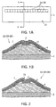
- a thermal head 1 has a plurality of heat generators 2A to 2N (N is a predetermined number) arranged in line on a head surface 1A perpendicularly to the traveling direction of a printing paper (not shown).
- Each of the heat generators 2A to 2N has a heat generation resistive element 5 on a protrusion of a glass layer 4 laminated on a ceramic substrate 3 as illustrated in a cross-sectional view taken along a line A-A' across the head surface 1A in Fig. 1B.
- the heat generation resistive element 5, together with electrodes 6 formed at one end and the other end thereof, is overlaid by a protective film 7 made of a glass material.
- the protective film 7 of the heat generators 2A to 2N corresponding to the damaged portion is likely to suffer a flaw 7A as illustrated in Fig. 2.
- the heat generation resistive element 5 changes its resistance value.
- an associated heat generation resistive element 5 is opened to break a current flow, resulting in a white line drawn on a printing paper along its traveling direction.
- Fig. 4 illustrates the relation between the resistance value of the heat generation resistive element 5 and the time change.
- a characteristic curve F1 of the heat generation resistive element 5 has a characteristic in which the resistance value of the heat generation resistive element 5 is R 0 at time T 0 , once decreases over time, and then gradually increases.
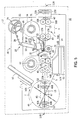
- a card printer to which the present invention is applied, is generally designated by reference numeral 10.
- a card material 13 inserted into the card printer from a card insertion slot 11A of a housing 11 through cleaning rollers 12A, 12B is carried by the card carrier 14 along a carrying path CR.
- the card material 13 employed in this embodiment conforms to the so-called International Organization for Standardization (ISO) standard. Specifically, the card material 13 has a magnetic stripe formed on one side along a longitudinal edge, and an Integrated Circuit (IC) memory embedded in the other side at a predetermined position near a front end of the card material 13.
- ISO International Organization for Standardization
- the card carrier 14 is composed of first and second carrying sections 14A, 14B disposed on front and back sides of a platen 15 along the carrying path CR.
- the first and second carrying sections 14A, 14B are provided with four pairs of carrying rollers 16A to 19A and 16B to 19B, respectively, which are mounted on axes for any rotation along the carrying path CR at predetermined intervals.
- the upper carrying rollers 16A to 19A are rotated in the same direction in association with each other according to the rotation of a driving motor (not shown), while the lower carrying rollers 16B to 19B are kept in contact with the corresponding upper carrying rollers 16A to 19A, so that the lower carrying rollers 16B to 19B are rotated in the direction opposite to the rotation of the upper carrying rollers 16A to 19A.
- the card material 13, inserted between the upper and lower carrying rollers 16A to 19A and 16B to 19B is carried forward or backward along the carrying path CR in accordance with the rotation of the upper carrying rollers 16A to 19A.
- a color image printing part 20 is disposed at a predetermined position opposing the platen 15 above the card carrier 14.
- a head holding mechanism 22 including a head part 21 is extended in a direction in which a thermal head 23 supported at a leading end of the head part 21 is pressed against the platen 15, and is retracted in a direction in which the thermal head 23 is brought away from the platen 15.
- the head holding mechanism 22 is constructed of a cam 25 which rotates on a driving shaft 24 of a head motor (not shown), and a link mechanism engaged with the cam 25 and including a shifter member 28, a connecting member 29 and a supporting member 30 with a rotating shafts 26, 27 as fixed links.
- the link mechanism 26 to 30 engaged with the cam 25 is extended in response to the driving of the head motor in a printing mode in order to press the thermal head 23 against the platen 15.
- the link mechanism 26 to 30 engaged with the cam 25 is retracted in response to the driving of head motor in order to bring the thermal head 23 away from the platen 15.
- the color image printing part 20 drives the head holding mechanism 22 to press the thermal head 23 against the platen 15 with a roll-shaped ink ribbon 33, supported by a supply reel 31 and a wind-up reel 32, and a card material 13 positioned on the platen 15 interposed in between. Subsequently, the thermal head 23 is heated in this state based on a predetermined image printing signal to thermal-transfer the ink on the ink ribbon 33 onto one side of the card material 13.
- the roll-shaped ink ribbon 33 is accommodated in a ribbon cassette 34.
- the ribbon cassette 34 is loaded capable of being removed between the color image printing part 20 and the platen 15 through a cassette insertion slot (not shown) formed on a side wall of the housing 11.
- the ink ribbon 33 includes color pigments of yellow Y, magenta M, cyan C and black K, each coated over at a predetermined length thereon as a pigment for one piece of the card material 13, followed by a film-like sheet L, as illustrated in Fig. 6. Further, a predetermined mark (not shown) is impressed at the head position for each page of the ink ribbon 33 in order that the head position of the ink ribbon 33 can be located by detecting the mark by an optical sensor (not shown) disposed on a running path of the ink ribbon 33.
- the supply real 31 is provided with a torque limiter (not shown) for applying a predetermined torque during rotation, so that the ink ribbon 33 is always applied with a back tension. Further, an optical sensor (not shown) is disposed near the supply real 31 for detecting the diameter of the rolled ink ribbon 33. And by detecting the tension of the ink ribbon 33, the winding state of the wind-up reel 32 can be controlled.
- a magnetic recording/reproducing part 40 is disposed below the carrying path CR in the second carrier 14B.
- a magnetic head 41 is exposed on the carrying path CR so as to be positioned side by side with the lower carrying roller 18B and contacted the upper carrying roller 18A only during recording and reproduction. And the magnetic head 41 is concealed below the carrying path CR other than during recording and reproduction.
- the magnetic recording/reproducing part 40 records information based on a predetermined recording signal on magnetic stripes (not shown) formed on one side of the card material 13, with the magnetic head 41 exposed on the carrying path CR. Subsequently, the magnetic recording/reproducing part 40 reproduces the recorded information to judge whether or not any recording errors are found on the magnetic stripes.
- Optical sensors 42, 43, 44 of photo-interrupter type are disposed on front and back sides of the first carrying section 14A and in front of the second carrying section 14B in order that the presence or absence of the card material 13 carried along the carrying path CR is detected.
- a rotary carrier 45 is disposed along the carrying path CR.
- the rotary carrier 45 has a rotary mechanism 46 supported on a rotating shaft 47 on which it can rotate in a direction indicated by an arrow r or in the opposite direction.
- the rotary mechanism 46 includes a first pair of flipper rollers 48A, 48B and a second pair of flipper rollers 49A, 49B. And each pair is capable of any rotation keeping a symmetrical position with the rotation shaft 47 in between.
- the flipper rollers 48A, 49A on an upper side each rotate in the same direction in conjunction with the rotation of the driving motors (not shown).
- the flipper rollers 48B, 49B on a lower side are each pressed against the corresponding flipper rollers 48a, 49A on the upper side, and rotate in the opposite direction to the rotation of the flipper rollers 48A, 49A.
- the card material 13 inserted between the first pair of flipper rollers 48A, 48B and/or between the second pair of flipper rollers 49A, 49B is carried forward or backward on the carrier path CR according to the rotation of the flipper rollers 48A, 49A on the upper side.
- the rotary carrier 45 holds the card material 13 carried from the second carrying section 14B in the rotary mechanism 46, and rotates the rotary mechanism 46 together with the card material 13 held therein over a predetermined angular distance in the direction indicated by the arrow r or in the opposite direction as required to position the rotary mechanism 46, so that the card material 13 is delivered in a predetermined direction determined by positioning.
- An IC recording/reproducing part 50 is disposed near the rotary carrier 45. As the card material 13 delivered from the rotary carrier 45 is inserted into an insertion slot 50A of the IC recording/reproducing part 50, each terminal of an IC memory (not shown) disposed on the other side of the card material 13 is brought into contact with an interface connector (not shown). As a result, the IC recording/reproducing part 50 records information based on a predetermined recording signal, and then reproduces the recorded information to judge whether or not any recording errors are found in the IC memory.
- An unacceptable card tray 51 is disposed near the rotary carrier 45.
- the rotary carrier 45 delivers a card material 13, which has been determined that no recording errors have been found in the magnetic recording/reproducing part 40 or in the IC recording/reproducing part 50, to an external card tray (not shown) through a card discharge slot 11B of the housing 11.
- a first optical sensor 52 and a second optical sensor 53 are disposed outside the first pair of flipper rollers 48A, 48B and outside the second pair of flipper rollers 49A, 49B (i.e., both in the centrifugal direction of the rotating shaft 47), respectively, for detecting the presence or absence of the card material 13 sent thereto along the carrying path CR.
- the card carrier 14, the color image printing part 20, the magnetic recording/reproducing part 40, the rotary carrier 45 and the IC recording/reproducing part 50 are each driven in predetermined states in accordance with the control of a CPU 61 which responds to instructions from a host computer 60 (Fig. 7), later described.
- Fig. 7 illustrates the circuit configuration of the color image printing part 20.
- predetermined image printing data D P is supplied from a host computer 60 through an interface (I/F) 62 and a Computer Interface (C/I) driver 63
- a memory controller 64 writes a one-frame portion of the image printing data D CP into corresponding frame memories 65 to 69 as color image printing data D PY (yellow Y), D PM (magenta M), D PC (cyan C) and D PK (black K), corresponding to the respective colors, and laminate data P DL (film-like sheet L) in accordance with the control of the CPU 61.
- the memory controller 64 reads the color image printing data D PY , D PM , D PC , D PK and the laminate data D PL from the respective frame memories 65 to 69 at predetermined timing in accordance with the control of the CPU 61. Then the color image printing data D PY , D PM , D PC are transmitted to color adjustment parts 70 to 72, respectively, and the color image printing data D PK and the laminate data D PL are transmitted to respective input terminals of a selector 73.
- the color adjustment parts 70 to 72 which are provided with a color conversion table (not shown) having standard image printing characteristics for each color, perform color adjustment for each color in accordance with an adjustment curve before and after color matching processing, and transmit resulting color image printing data D PY1 , D PM1 , D PC1 to a masking part 74.
- the masking part 74 separates unnecessary data from the supplied color image printing data D PY1 , D PM1 , D PC1 and transmits resulting color image printing data D PY2 , D PM2 , D PC2 to the other input terminal of the selector 73.
- the selector 73 sequentially transmits data selected as required from the respective color image printing data D PY2 , D PM2 , D PC , D PK and the laminate data D PL , supplied thereto, based on the control of the CPU 61 to a gamma correction part 75.
- the gamma correction part 75 performs a color-strength electrification time conversion with a predetermined heat correction coefficient which has been set on the basis of the control of the CPU 61, and supplies a head controller 76 with print image data D T resulting from the conversion.
- the head controller 76 which is disposed in the head holding mechanism 22, converts the print image data D T to a current signal D I which is then provided to the thermal head 23.
- a plurality of heat generation resistive elements arranged on a head surface (not shown) of the thermal head 23 are heated in accordance with the current signal D I . Consequently, the color image printing part 20 can heat the head surface of the thermal head 23 based on the image printing data D P , and print a desired color image in accordance with the image print data D P based on the heated head on one or the other side of the card material 13.
- the CPU 61 can move the thermal head 23 in the head part 22 closer to or away from the platen 15 by controlling the driving of mechanical controller 77 including the aforementioned cam 25 and the link mechanism 26 to 30, described in Fig. 5.
- the CPU 61 also sends control instructions to respective circuits through a bus 78.
- the color image printing part 20 is provided with a head diagnosis part 80 between the CPU 61 and the thermal head 23.
- the head diagnosis part 80 sequentially measures the resistance value of each heat generation resistive element one by one for a plurality of heat generators (not shown) disposed on the head surface of the thermal head 23 in order to permit judgement as to whether or not the resistance value of each heat generation resistive element is normal based on the results of the measurements.
- the CPU 61 first sends a switching signal S1 to the head diagnosis part 80 to selectively switch the head diagnosis part 80 to a printing mode or a head diagnosis mode.
- the head controller 76 sends electrification setting data D E to the thermal head 23 for sequentially measuring one by one the resistance value of the heat generation resistive elements corresponding to the respective heat generators of the thermal head 23 in accordance with the control of the CPU 61.
- the thermal head 23 has a plurality of heat generators 23H 1 to 23H N (N is for example equal to 640) on the head surface.
- the heat generators 23H 1 to 23H N are connected by a latch circuit 90 to a plurality of registers 91R 1 to 91R N , which constitute a serial-type shift register.
- Image printing data D I are orderly stored one by one in the plurality of registers 91R 1 to 91R N in synchronization with a clock CL inputted thereto.
- all outputs of the 91R 1 to 91R N are applied in parallel to the latch circuit 90.
- Respective heat generators 23H 1 to 23H N are connected to a common power supply 94 through heat generation resistive elements 93R 1 to 93R N which basically comprise transistors 92Q 1 to 92Q N , respectively, each of which has a collector connected to a load resistor. All emitters are connected to a common terminal (not shown) in the head diagnosis part 80. And bases are connected to each output stage of the latch circuit 90 through load resistors 95R 1 to 95R N , respectively.
- the latch circuit 90 upon receiving the electrification setting data D E supplied from the head controller 76, sequentially electrifies and connects one by one between a heat generator 23H I (I is an arbitrary number satisfying 1 ⁇ I ⁇ N) and a corresponding register 91R I , thereby sequentially turning on a transistor 92Q I in the heat generator 23H I .
- This causes a voltage of the power supply 94 to be applied to each heat generator 23H I , and a collector-emitter current to flow through a corresponding heat generation resistive element 93R I into the head diagnosis part 80.
- the head diagnosis part 80 has a configuration based on an operational amplifier 100, as illustrated in Fig. 9, which has one input terminal connected to the thermal head 23, to a drain of a power Metal Oxide Semiconductor (MOS) Field Effect Transistor (FET) 101 and to a load resistor 102R, and the other input terminal is connected to a reference voltage source 103.
- MOS Metal Oxide Semiconductor
- FET Field Effect Transistor
- a source of the power MOS FET 101, the load resistor 102R and the reference voltage source 103 are connected to a ground GND.
- the power MOS FET 101 is used as a switching circuit which turns on or off in response to "H” or "L” level of the switching signal S1 supplied from the CPU 61 to the gate thereof.
- the CPU 61 supplies the power MOS FET 101 with the switching signal S1 at "L" level to cause the power MOS FET 101 to turn OFF, the current supplied from each heat generator 23H I does not flow through the drain-source of the power MOS FET 101 but flows through the intermediate connection point P1 into the one input terminal of the operational amplifier 100 as well as through the load resistor 102R to the ground GND.
- the operational amplifier 100 calculates the difference in potential between the one input terminal and the other input terminal, subsequently converts the differential voltage to a digital form through an analog-to-digital (A/D) converter circuit 104, and sends the digital product to the CPU 61 as differential voltage data D VS .
- A/D analog-to-digital
- the operational amplifier 100 is composed of a differential amplifier circuit 110 as a basic component, and a current regulating circuit 111 connected thereto, as illustrated in Fig. 10.
- the differential amplifier circuit 110 has a pair of PNP transistors Q1, Q2, which have their bases connected to the power supply 94 through a heat generation resistive element 93R I of the heat generator 23H I and a load resistor 113R which has the same resistance value as the heat generation resistive element 93R I , respectively.
- An intermediate connection point P2 between the base of the transistor Q2 and the load resistor 113R is connected to an end of a voltage dividing resistor 114R which has the same resistance value as the load resistor 102R and has the other end connected to the ground GND.
- the reference voltage source 103 mentioned above in connection with Fig. 9 is actually composed of the resistors 113R, 114R connected in series between the power supply 94 and the ground GND, and the differential amplifier 110 connected to the intermediate connection point P2 between the resistors 113R and 114R.
- the transistor Q1 has a collector connected to the ground GND, while the transistor Q2 has a collector connected through a voltage dividing resistor 115R to the ground GND.
- An intermediate connection point P3 between the collector of the transistor Q2 and the resistor 115R is connected to the A/D converter circuit 104.
- the current regulating circuit 111 has a pair of PNP transistors Q3, Q4, which have their emitters connected commonly to the power supply 94 through load resistors 116R, 117R. Bases of the transistors Q3, Q4 are connected to one end of a capacitor C1, the other end of which is connected to the power supply 94, and also connected through a load resistor 118R to the ground GND. Thus, the current regulating circuit 111 is configured in order that the same current as that flowing into the transistor Q4 flows into the transistor Q3.
- the transistor Q3 has its collector connected through load resistors 119R, 120R commonly to emitters of the transistors Q1, Q2 in the differential amplifier circuit 110, respectively.
- the intermediate connection points P1, P2 both have the same potential difference, so that a differential voltage value outputted from the differential amplifier circuit 110 through the intermediate connection point P3 is applied as it is to the A/D converter circuit 104.
- the resistance value r I of the heat generation resistive element 93R I is higher than the set standard range to reduce the potential at the intermediate connection point P1
- a current flowing into the base of the transistor Q1 decreases, causing an emitter-collector current of the transistor Q1 to decrease.
- a current flowing from the current regulating circuit 111 is regular, a reduced portion of the emitter-collector current of the transistor Q1 is added to an emitter-collector current of the transistor Q2 to increase the same.
- the potential difference at the intermediate connection point P3 is increased and applied to the A/D converter circuit 104.
- the resistance value r I of the heat generation resistive element 93R I is lower than the set standard range to increase the potential at the intermediate connection point P1
- a current flowing into the base of the transistor Q1 increases, causing the emitter-collector current of the transistor Q1 to increase.
- the increased emitter-collector current of the transistor Q1 is subtracted from the emitter-collector current of the transistor Q2 to reduce the same.
- the potential difference at the intermediate connection point P3 is reduced and applied to the A/D converter circuit 104.
- the thermal head 23 when the thermal head 23 is applied with the electrification setting data D E , a current flows through the heat generation resistive element 93R I disposed in each heat generator 23H I within the thermal head 23 to generate a drop voltage V I across the heat generation resistive element 93R I .
- the head diagnosis part 80 calculates a difference between the voltage V I and the voltage V M of the reference voltage source 103 and converts the calculated difference to a digital form to produce differential voltage data D VS which is sent to the CPU 61.
- the CPU 61 also contains a predetermined conversion table (not shown), such that the resistance value r I of the heat generation resistive element 93R I corresponding to the differential voltage data D VS can be retrieved from the conversion table based on a characteristic curve F2 which represents the resistance value r I of the heat generation resistive element 93R I in proportion to the voltage of the differential voltage data D VS , as illustrated in Fig. 11.
- the CPU 61 sequentially retrieves from the conversion table the resistance value r I of the heat generation resistive element 93R I corresponding to the differential voltage data D VS sequentially supplied from the head diagnosis part 80 based on the differential voltage data D VS , and then stores the retrieved resistance value r I in a flash memory 81.
- the flash memory 81 previously stores initial resistance value (the resistance value measured when they were manufactured) r 0I of all the heat generation resistive elements 93R I , and also stores the resistance value r I of all the heat generation resistive elements 93R I measured in the previous head diagnosis mode.
- the CPU 61 judges that the resistance value r I of a heat generation resistive element 93R I corresponding to a voltage of differential voltage data D VS supplied from the head diagnosis part 80 is out of a predetermined range with respect to the characteristic curve F2 illustrated in Fig. 11, the CPU 61 sends a printing reference signal S2 to the host computer 60 through the C/I driver 63 and the interface 62 as required (Fig. 7).
- the host computer 60 upon receipt of the printing reference signal S2, judges whether or not a heat generator 23H I within the thermal head 23 exhibiting an abnormal electrification state actually is used for an image printing area based on image printing data D P within an image to be printed, and sends a diagnosis notification signal S3 in accordance with the result of the judgement to the CPU 61 through the interface and the C/I driver.
- the host computer 60 sends to an error display part 82 an error signal S4 indicating that the thermal head 23 has failed, when the result of the judgement is negative, thereby causing the error display part 82 to display on its display screen that the thermal head 23 has failed.
- the CPU 61 in the color image printing part 20 executes a head diagnosis processing procedure RT1 illustrated in Figs. 12, 13 based on the control of the host computer 60, to diagnose whether or not each of heat generators 23H 1 to 23H N , arranged on the surface of the thermal head 23, exhibits an abnormal electrification state by sequentially measuring one by one the resistance value of the heat generation resistive elements 93R 1 to 93R N within the respective heat generators 23H 1 to 23H N .
- the CPU 61 enters the head diagnosis processing procedure RT1 illustrated in Fig. 12 from step SP0 in accordance with the control of the host computer 60, before starting a printing operation or after ending a printing operation, that is, when not in the printing mode.
- the CPU 61 turns off the power MOS FET 101 to set the head diagnosis mode.
- the CPU 61 proceeds to step SP2, where the CPU 61 sequentially electrifies one by one the heat generation resistive elements 93R 1 to 93R N in the plurality of heat generators 23H 1 to 23H N of the thermal head 23.
- step SP3 where for one of the heat generators 23H I (1 ⁇ I ⁇ N), a current flowing into the intermediate connection point P1 from the power supply 94 through the head generation resistive element 93R I and a current flowing from the reference voltage source 103 are applied to one input terminal and the other input terminal, respectively, of the operational amplifier 100 in the head diagnosis unit 80 illustrated in Fig. 9, to force the operational amplifier 100 to calculate the difference between the voltage V I at the intermediate connection point P1 and the voltage V M of the reference voltage source 103. Then, the CPU 61 receives the differential voltage.
- the CPU 61 retrieves the resistance value r I of the heat generation resistive element 93R I corresponding to the received differential voltage in accordance with the predetermined conversion table (not shown) stored therein.
- the CPU 61 determines whether or not the retrieved resistance value r I of the heat generation resistive element 93R I is within a predetermined range with respect to the characteristic curve F2 in the aforementioned Fig. 11.
- step SP5 If a negative result is returned at step SP5, this means that the heat generation resistive element 93R I is in an open state or in a short-circuited state, in which case the CPU 61 proceeds to step SP6, where it further judges whether or not the resistance value r I is higher than the predetermined range with respect to the characteristic curve F2.
- step SP6 If an affirmative result is returned at step SP6, this means that the heat generation resistive element 93R I is in a short-circuited state, in which case the CPU 61 proceeds to step SP7 (Fig. 13), later described, where it notifies the host computer 60 of the fact that the heat generation resistive element 93R I exhibits an abnormal electrification state.
- step SP6 if a negative result is returned at step SP6, this means that the heat generation resistive element 93R I is in an open state, in which case the CPU 61 proceeds to step SP8, where the CPU 61 forces the host computer 60 to judge whether or not the heat generation resistive element 93R I is actually a heat generation resistive element R I of a heat generator 23H I falling into an image printing area based on image printing data D P within an image to be printed.
- step SP8 If an affirmative result is returned at step SP8, this means that the heat generator 23H I does affect the contents to be printed on a card material 13, in which case the CPU 61 proceeds to step SP7, where it notifies the host computer 60 of the fact that the heat generation resistive element 93R I exhibits an abnormal electrification state, as mentioned above.
- step SP8 determines that the heat generation resistive element 93R I is in a normal electrification state since the contents to be printed on the card material 13 will not be affected by the heat generation resistive element 93R I even if it is in an open state. Then, the CPU 61 proceeds to step SP9 (Fig. 13), later described.
- step SP5 if an affirmative result is returned, this means that the resistance value of the heat generation resistive element 93R I retrieved from the conversion table is within the predetermined range with respect to the characteristic curve F2, in which case the CPU 61 proceeds to step SP10, where it reads from the flash memory 81 the resistance value r I ' of the heat generation resistive element 93R I measured in the preceding head diagnosis mode, and an initial resistance value r 0I of the heat generation resistive element 93R I at the time of manufacturing.
- the CPU 61 calculates a changing rate A I of the resistance value r I of the heat generation resistive element 93R I measured at this time to the resistance value r I ' of the heat generation resistive element 93R I measured at the preceding time as represented by the following expression (2):
- a I
- step SP12 determines whether or not the difference between the changing rate A I and a changing rate A I ' which is calculated in the preceding head diagnosis mode is equal to or less than a predetermined value. If a negative result is returned, this means that it is highly likely that the heat generation resistive element 93R I falls into an abnormal electrification state.
- the CPU 61 proceeds to step SP13 illustrated in Fig. 13, where it judges whether the changing rate A I exceeds a predetermined value which is set as an abnormal changing rate.
- step SP13 If a negative result is returned at step SP13, this means that the difference between the changing rate A I and the previously calculated changing rate A I ' is equal to or more than the predetermined value and equal to or less than the predetermined value above which an abnormal changing rate is identified.
- the CPU 61 proceeds to step SP14, where it sets a flag representative of a warning (hereinafter referred to as the "warning flag") in the flash memory 81 in order to register that the heat generation resistive element 93R I is less likely to fall into an abnormal electrification state at this time.
- the warning flag hereinafter referred to as the "warning flag
- step SP15 judges whether or not a warning flag has been set in the flash memory 81 for the heat generation resistive element 93R I in the preceding head diagnosis mode.
- step SP15 If an affirmative result is returned at step SP15, this means that the heat generation resistive element 93R I has been likely to fall into an abnormal electrification state not only at the preceding time but also at the present time.
- the CPU 61 proceeds to step SP7, where it judges in the foregoing manner that the heat generation resistive element 93R I has been in an abnormal electrification state, and notifies the host computer 60 of this fact.
- step SP15 if a negative result is returned at step SP15, this means that the heat generation resistive element 93R I could exhibit for the first time an abnormal electrification state in the current head diagnosis mode, in which case the CPU 61 proceeds to step SP9.
- step SP12 illustrated in Fig. 12 if an affirmative result is returned, this means that the difference between the changing rate A I and a changing rate A I ' which is calculated in the preceding head diagnosis mode of the heat generation resistive element 93 R I is equal to or less than the predetermined value, and accordingly the heat generation resistive element 93R I exhibits a normal electrification state, in which case the CPU 61 proceeds to step SP16 (Fig. 13), where it overwrites the current resistance value r I and the changing rate A I of the heat generation resistive element 93R I in the flash memory 81.
- the thermal head 23 is likely to fall into a fault if the resistance value r I of the heat generation resistive element 93R I takes a value out of the predetermined range with respect to the initial resistance r 0I .
- the CPU 61 proceeds to step SP17, where it judges whether or not the difference between the resistance value r I and the initial resistance value r 0I is equal to or less than a predetermined value.
- step SP17 the CPU 61 proceeds to step SP7, where it notifies the host computer 60 of the fact that the heat generation resistive element 93R I exhibits an abnormal electrification state, similarly to the above.
- the host computer 60 upon receipt of the notification from the CPU 61, displays on the display screen of the error display part 82 that the thermal head 23 is faulty or likely to fall into a fault.
- step SP17 if an affirmative result is returned at step SP17, this means that the heat generation resistive element 93R I is in a normal electrification state, in which case the CPU 61 proceeds to step SP9, where it judges whether the heat generation resistive element 93R I is the last electrified heat generation resistive element 93R N .
- step SP9 the CPU 61 judges that the diagnosis has been completed for all the heat generation resistive elements 93R 1 to 93R N as to whether or not they exhibit an abnormal electrification state, and then proceeds immediately to step SP18 to terminate the head diagnosis processing procedure RT1.
- step SP9 the CPU 61 again returns to step SP3, where it executes the processing from step SP3 to step SP17 for the next electrified heat generation resistive element 93R I+1 as described above, and repeats this processing until an affirmative result is returned at step SP9.
- the heat generation resistive elements 93R 1 to 93R N in the plurality of heat generators 23H 1 to 23H N arranged on the surface of the thermal head 23 are sequentially electrified one by one, and the resistance value of the heat generation resistive elements 93R 1 to 93R N is measured respectively to determine whether or not each of the heat generation resistive elements 93R I (1 ⁇ I ⁇ N) is open or short-circuited based on the resistance value r I thereof during the head diagnosis mode.
- the changing rate A I of the heat generation resistive element 93R I is calculated on the basis of the resistance value r I ' of the heat generation resistive element 93R I measured at the preceding time and the resistance value r I corresponding thereto measured at the current time. It can be determined on the basis of each changing rate A I whether or not the associated heat generation resistive element 93R I is currently in a normal electrification state or is likely to suffer a fault in future, before actually entering a printing stage.
- each heat generation resistive element 93R I is determined to be normal at present, it can be judged whether or not the thermal head 23 is faulty or is likely to fall into a fault in accordance of the difference between the changing rate A I of the heat generation resistive element R I and the previously calculated changing rate A I ' of the heat generation resistive element 93R I ' corresponding thereto.
- the heat generation resistive elements 93R 1 to 93R N within the plurality of heat generators 23H 1 to 23H N arranged on the surface of the thermal head 23 are sequentially electrified one by one before starting a printing operation or after ending a printing operation. Then, the changing rate A I is calculated on the basis of the previously measured resistance value r I ' of each heat generation resistive element 93R I (1 ⁇ I ⁇ N) and the corresponding resistance value r I measured at the current time.
- the CPU 61 judges the host computer 60 of this fact as the predetermined error processing, so that the host computer 60 forces the error display part 82 to display on its display screen that the thermal head 23 is faulty or is likely to fall into a fault.
- the present invention is not limited thereto.
- the CPU 61 can bring the color image printing part 20 into a printing stop state instead of or in addition to notifying the host computer 60 of the fact. In this case, even if the color image printing part 20 is switched to a printing mode, it is possible to obviate printing errors on a card material 13 since the color image printing part 20 is in the printing stop state.
- the CPU 61 sends a printing reference signal S2 to the host computer 60 so that the host computer 60 judges whether or not the heat generation resistive element 93R X is actually a heat generation resistive element which corresponds to an image printing area based on image printing data D P within an image to be printed.
- the present invention is not limited thereto.
- a frame memory (not shown) for storing an image based on the image printing data D P so that the CPU 61 makes the above-mentioned determination based on the image printing data D P read from the frame memory, without intervention of the host computer 60.
- the CPU 61 uses a predetermined conversion table to retrieve the resistance value of each heat generation resistive element 93R I (1 ⁇ I ⁇ N) corresponding to differential voltage data D VS supplied from the head diagnosis part 80.
- the present invention is not limited thereto.
- the CPU 61 does inverse calculating differential voltage data D VS outputted from the head diagnosis part 30 to derive the resistance value of each heat generation resistive element 93R I .
- a wide variety of other configurations can be applied as measuring means as long as it can measure the resistance value of each electrified heat generation resistive element 93R I .
- the CPU 61 serving as calculation means, calculates the change rate A I for the resistance value of each heat generation resistive element 93RI based on the resistance value r I ' of each heat generation resistive element 93R I previously measured in the head diagnosis part 80 and the resistance value r I of each heat generation resistive element 93R I measured at this time.
- the present invention is not limited thereto. Alternatively, a wide variety of other configurations can be applied as the calculating means.
- the CPU 61 serving as diagnosis means, relies on the change rate A I for the resistance value r I of each heat generation resistive element 93R I to jugde a electrification state of the corresponding heat generation resistive element 93R I , and with the result of the judgement judges the condition of the thermal head 23 in accordance.
- the present invention is not limited thereto.
- the host computer 60 can be used as the diagnosis means, or a wide variety of other configurations can be applied as the diagnosis means, as long as it can readily judge, before actually entering a printing stage, whether or not each heat generation resistive element 93RI is currently in a normal electrification state, or whether or not a fault is currently occurring, or whether or not a fault is likely to occur in future.
- the flash memory 81 is used as storage means for storing the resistance value r I of each heat generation resistive element 93R I measured in the head diagnosis part 80.
- the present invention is not limited thereto, but a variety of configurations can be applied including, for example, electrically erasable programmable read only memory (EEPROM), static random access memory (static RAM), or the like.
- EEPROM electrically erasable programmable read only memory
- static RAM static random access memory
- the card material 13 in accordance with the ISO standard is used as a printing medium
- the present invention is not limited thereto.
- a card material in accordance with Japan Industrial Standard (JIS) can be used.
- the present invention can also be applied to a variety of card materials, which do not have an IC card and/or magnetic stripes.
- a thermal head diagnosis method for diagnosing the condition of a thermal head first measures respectively the resistance value of a plurality of heat generation resistive elements arranged on a head surface of the thermal head, and then calculates a change amount of the resistance value of each heat generation resistive element based on the resistance value of each heat generation resistive element measured in the past, and the resistance value of each heat generation resistive elements measured at the current time to determine a electrification state of each heat generation resistive element based on the calculation result for diagnosing the condition of the thermal head in accordance with the judgement result, thereby making it possible to diagnose the condition of the thermal head before entering a printing stage. Consequently, it is possible to realize a head diagnosis method which is capable of efficiently preventing printing errors.
Landscapes
- Electronic Switches (AREA)
- Accessory Devices And Overall Control Thereof (AREA)
Applications Claiming Priority (2)
| Application Number | Priority Date | Filing Date | Title |
|---|---|---|---|
| JP21417998 | 1998-07-29 | ||
| JP21417998A JP2000043307A (ja) | 1998-07-29 | 1998-07-29 | ヘッド診断装置及びヘッド診断方法 |
Publications (2)
| Publication Number | Publication Date |
|---|---|
| EP0982134A2 true EP0982134A2 (fr) | 2000-03-01 |
| EP0982134A3 EP0982134A3 (fr) | 2000-09-20 |
Family
ID=16651555
Family Applications (1)
| Application Number | Title | Priority Date | Filing Date |
|---|---|---|---|
| EP99114794A Withdrawn EP0982134A3 (fr) | 1998-07-29 | 1999-07-28 | Appareil et procédé pour le diagnostic de défauts d'une tête imprimante |
Country Status (4)
| Country | Link |
|---|---|
| EP (1) | EP0982134A3 (fr) |
| JP (1) | JP2000043307A (fr) |
| CN (1) | CN1106944C (fr) |
| CA (1) | CA2278881A1 (fr) |
Cited By (5)
| Publication number | Priority date | Publication date | Assignee | Title |
|---|---|---|---|---|
| WO2002055310A1 (fr) * | 2001-01-09 | 2002-07-18 | Encad, Inc. | Systeme et procede de gestion de la qualite d'une tete d'impression a jet d'encre |
| EP1658982A2 (fr) * | 2004-11-20 | 2006-05-24 | Samsung Electronics Co., Ltd. | Tête d'impression thermique |
| EP2100742A1 (fr) * | 2008-03-14 | 2009-09-16 | Custom Engineering SpA | Dispositif de contrôle d'impression pour imprimante thermique |
| EP2360022A1 (fr) * | 2008-12-12 | 2011-08-24 | Shandong New Beiyang Information Technology Co., Ltd. | Dispositif et procédé de détection de tête d'impression thermique et imprimante thermique les utilisant |
| CN102189812A (zh) * | 2010-01-22 | 2011-09-21 | 精工爱普生株式会社 | 头元件的动作确认机构及方法和头元件数确认方法 |
Families Citing this family (8)
| Publication number | Priority date | Publication date | Assignee | Title |
|---|---|---|---|---|
| JP6679941B2 (ja) * | 2016-01-14 | 2020-04-15 | セイコーエプソン株式会社 | 印刷装置、制御方法、及び、印刷システム |
| JP2017119413A (ja) * | 2015-12-25 | 2017-07-06 | セイコーエプソン株式会社 | 印刷装置、制御方法、及び、印刷システム |
| JP6679982B2 (ja) * | 2015-12-25 | 2020-04-15 | セイコーエプソン株式会社 | 印刷装置、及び、制御方法 |
| WO2019212511A1 (fr) | 2018-04-30 | 2019-11-07 | Hewlett-Packard Development Company, L.P. | Détermination de frappe potentielle de tête d'impression |
| JP7263877B2 (ja) * | 2019-03-27 | 2023-04-25 | ブラザー工業株式会社 | 印刷装置 |
| CN110789236B (zh) * | 2019-11-06 | 2020-09-25 | 上海商米科技集团股份有限公司 | 热敏打印机的打印头坏点检测方法 |
| CN110861412A (zh) * | 2019-11-28 | 2020-03-06 | 湖南凯通电子有限公司 | 一种印字机 |
| JP2022179919A (ja) * | 2021-05-24 | 2022-12-06 | セイコーエプソン株式会社 | 印刷装置及び印刷物の生産方法 |
Citations (5)
| Publication number | Priority date | Publication date | Assignee | Title |
|---|---|---|---|---|
| JPS60159662A (ja) * | 1984-01-31 | 1985-08-21 | Tokyo Electric Co Ltd | サ−マルヘツドの発熱体故障検出装置 |
| US4769657A (en) * | 1985-08-29 | 1988-09-06 | Kabushiki Kaisha Sato | Fault detection device for thermal printing head heating circuits |
| EP0394699A1 (fr) * | 1989-04-24 | 1990-10-31 | Lexmark International, Inc. | Appareil et méthode pour détecter les éléments de chauffage défectueux dans les imprimantes à jet d'encre |
| US5469068A (en) * | 1992-09-01 | 1995-11-21 | Fuji Photo Film Co., Ltd. | Thermal printer and device and method for measuring resistance of thermal head of thermal printer |
| US5546112A (en) * | 1994-10-28 | 1996-08-13 | Pitney Bowes Inc. | Epm having a system for detecting fault conditions of the thermal printhead |
Family Cites Families (5)
| Publication number | Priority date | Publication date | Assignee | Title |
|---|---|---|---|---|
| US5608333A (en) * | 1993-06-18 | 1997-03-04 | Fuji Photo Film Co., Ltd. | Method of driving heating element to match its resistance, thermal printer, and resistance measuring device |
| JP3310788B2 (ja) * | 1994-09-02 | 2002-08-05 | 富士写真フイルム株式会社 | サーマルヘッドの抵抗値測定装置及びサーマルプリンタ |
| JPH0958041A (ja) * | 1995-08-29 | 1997-03-04 | Tec Corp | サーマルプリンタ |
| JP3590702B2 (ja) * | 1995-11-16 | 2004-11-17 | 富士写真フイルム株式会社 | サーマルヘッドの抵抗データ測定方法及び装置並びにこれを備えたサーマルプリンタ |
| JPH10100465A (ja) * | 1996-09-27 | 1998-04-21 | Sanyo Electric Co Ltd | サーマルヘッドの温度測定用抵抗体基板、サーマルヘッドの温度測定装置およびサーマルヘッドの温度測定装置を備えるサーマルプリンタ |
-
1998
- 1998-07-29 JP JP21417998A patent/JP2000043307A/ja active Pending
-
1999
- 1999-07-26 CA CA 2278881 patent/CA2278881A1/fr not_active Abandoned
- 1999-07-28 EP EP99114794A patent/EP0982134A3/fr not_active Withdrawn
- 1999-07-29 CN CN99111863A patent/CN1106944C/zh not_active Expired - Fee Related
Patent Citations (5)
| Publication number | Priority date | Publication date | Assignee | Title |
|---|---|---|---|---|
| JPS60159662A (ja) * | 1984-01-31 | 1985-08-21 | Tokyo Electric Co Ltd | サ−マルヘツドの発熱体故障検出装置 |
| US4769657A (en) * | 1985-08-29 | 1988-09-06 | Kabushiki Kaisha Sato | Fault detection device for thermal printing head heating circuits |
| EP0394699A1 (fr) * | 1989-04-24 | 1990-10-31 | Lexmark International, Inc. | Appareil et méthode pour détecter les éléments de chauffage défectueux dans les imprimantes à jet d'encre |
| US5469068A (en) * | 1992-09-01 | 1995-11-21 | Fuji Photo Film Co., Ltd. | Thermal printer and device and method for measuring resistance of thermal head of thermal printer |
| US5546112A (en) * | 1994-10-28 | 1996-08-13 | Pitney Bowes Inc. | Epm having a system for detecting fault conditions of the thermal printhead |
Non-Patent Citations (1)
| Title |
|---|
| PATENT ABSTRACTS OF JAPAN vol. 009, no. 334 (P-417), 27 December 1985 (1985-12-27) & JP 60 159662 A (TOKYO DENKI KK), 21 August 1985 (1985-08-21) * |
Cited By (11)
| Publication number | Priority date | Publication date | Assignee | Title |
|---|---|---|---|---|
| WO2002055310A1 (fr) * | 2001-01-09 | 2002-07-18 | Encad, Inc. | Systeme et procede de gestion de la qualite d'une tete d'impression a jet d'encre |
| US6866359B2 (en) | 2001-01-09 | 2005-03-15 | Eastman Kodak Company | Ink jet printhead quality management system and method |
| EP1658982A2 (fr) * | 2004-11-20 | 2006-05-24 | Samsung Electronics Co., Ltd. | Tête d'impression thermique |
| EP1658982A3 (fr) * | 2004-11-20 | 2007-10-17 | Samsung Electronics Co., Ltd. | Tête d'impression thermique |
| EP2100742A1 (fr) * | 2008-03-14 | 2009-09-16 | Custom Engineering SpA | Dispositif de contrôle d'impression pour imprimante thermique |
| EP2360022A1 (fr) * | 2008-12-12 | 2011-08-24 | Shandong New Beiyang Information Technology Co., Ltd. | Dispositif et procédé de détection de tête d'impression thermique et imprimante thermique les utilisant |
| EP2360022A4 (fr) * | 2008-12-12 | 2013-06-26 | Shandong New Beiyang Inf Tech | Dispositif et procédé de détection de tête d'impression thermique et imprimante thermique les utilisant |
| CN102189812A (zh) * | 2010-01-22 | 2011-09-21 | 精工爱普生株式会社 | 头元件的动作确认机构及方法和头元件数确认方法 |
| EP2347907A3 (fr) * | 2010-01-22 | 2011-10-19 | Seiko Epson Corporation | Mécanisme de vérification de l'opération d'un élément de tête, procédé de vérification de l'opération d'un élément de tête et procédé de vérification du numéro d'un élément de tête |
| US8654161B2 (en) | 2010-01-22 | 2014-02-18 | Seiko Epson Corporation | Head element operation check mechanism, head element operation check method, and head element number check method |
| CN102189812B (zh) * | 2010-01-22 | 2014-08-06 | 精工爱普生株式会社 | 头元件数确认机构和头元件数确认方法 |
Also Published As
| Publication number | Publication date |
|---|---|
| CA2278881A1 (fr) | 2000-01-29 |
| JP2000043307A (ja) | 2000-02-15 |
| CN1106944C (zh) | 2003-04-30 |
| EP0982134A3 (fr) | 2000-09-20 |
| CN1243068A (zh) | 2000-02-02 |
Similar Documents
| Publication | Publication Date | Title |
|---|---|---|
| EP0982134A2 (fr) | Appareil et procédé pour le diagnostic de défauts d'une tête imprimante | |
| JPH0655750A (ja) | サーマルプリンタ | |
| US7391334B2 (en) | Connection checking system, printer device, method of checking connected state, connection checking program, and recording medium storing connection checking program | |
| CN100471679C (zh) | 通过检测热打印头类型来形成图像的装置和方法 | |
| JP2650949B2 (ja) | 液晶表示装置 | |
| US5684931A (en) | Label printer, such as a thermal printer for printing labels | |
| JP2523625B2 (ja) | プリンタ装置 | |
| JP2005153416A (ja) | サーマルヘッドのスジ印画補正方法及び装置、及びサーマルヘッド及びサーマルプリンタ | |
| JPH09300682A (ja) | 印字装置および自動改札機 | |
| JPH09218619A (ja) | ユニット寿命監視機構 | |
| JPS6092875A (ja) | サ−マルプリンタ | |
| JPH0250849A (ja) | サーマルヘッドの発熱回路不良検出装置 | |
| JP2001105703A (ja) | 熱転写リボンカセット | |
| JP4691859B2 (ja) | カードリーダ | |
| JPH03128257A (ja) | カード対応機の印字装置 | |
| US20070229088A1 (en) | Failure display unit and disk drive device with failure display function | |
| JPS62124966A (ja) | 感熱転写記録装置 | |
| JPH0896092A (ja) | 媒体処理装置 | |
| JP4151283B2 (ja) | カードリーダ | |
| JPS63178063A (ja) | 感熱記録装置 | |
| JP2021092716A (ja) | 液晶装置及び液晶装置の検査方法 | |
| JPH0752422A (ja) | 可逆性感熱式記録媒体の消色装置 | |
| WO1992016912A1 (fr) | Carte magnetique du type a impression et dispositif de lecture/ecriture | |
| JP2001134133A (ja) | 画像形成装置 | |
| JPH0239951A (ja) | 通電熱転写プリンターにおける画像記録方法 |
Legal Events
| Date | Code | Title | Description |
|---|---|---|---|
| PUAI | Public reference made under article 153(3) epc to a published international application that has entered the european phase |
Free format text: ORIGINAL CODE: 0009012 |
|
| AK | Designated contracting states |
Kind code of ref document: A2 Designated state(s): DE ES FR GB IT |
|
| AX | Request for extension of the european patent |
Free format text: AL;LT;LV;MK;RO;SI |
|
| PUAL | Search report despatched |
Free format text: ORIGINAL CODE: 0009013 |
|
| AK | Designated contracting states |
Kind code of ref document: A3 Designated state(s): AT BE CH CY DE DK ES FI FR GB GR IE IT LI LU MC NL PT SE |
|
| AX | Request for extension of the european patent |
Free format text: AL;LT;LV;MK;RO;SI |
|
| RIC1 | Information provided on ipc code assigned before grant |
Free format text: 7B 41J 2/05 A, 7B 41J 2/35 B |
|
| 17P | Request for examination filed |
Effective date: 20010320 |
|
| AKX | Designation fees paid |
Free format text: DE ES FR GB IT |
|
| STAA | Information on the status of an ep patent application or granted ep patent |
Free format text: STATUS: THE APPLICATION IS DEEMED TO BE WITHDRAWN |
|
| 18D | Application deemed to be withdrawn |
Effective date: 20050201 |