EP0977262A2 - Integrierter Halbleiterchip mit modularen Füllstrukturen - Google Patents
Integrierter Halbleiterchip mit modularen Füllstrukturen Download PDFInfo
- Publication number
- EP0977262A2 EP0977262A2 EP99112844A EP99112844A EP0977262A2 EP 0977262 A2 EP0977262 A2 EP 0977262A2 EP 99112844 A EP99112844 A EP 99112844A EP 99112844 A EP99112844 A EP 99112844A EP 0977262 A2 EP0977262 A2 EP 0977262A2
- Authority
- EP
- European Patent Office
- Prior art keywords
- substrate
- areas
- semiconductor chip
- polysilicon
- filling structures
- Prior art date
- Legal status (The legal status is an assumption and is not a legal conclusion. Google has not performed a legal analysis and makes no representation as to the accuracy of the status listed.)
- Withdrawn
Links
Images

Classifications
-
- H—ELECTRICITY
- H10—SEMICONDUCTOR DEVICES; ELECTRIC SOLID-STATE DEVICES NOT OTHERWISE PROVIDED FOR
- H10D—INORGANIC ELECTRIC SEMICONDUCTOR DEVICES
- H10D84/00—Integrated devices formed in or on semiconductor substrates that comprise only semiconducting layers, e.g. on Si wafers or on GaAs-on-Si wafers
-
- H10W20/40—
Definitions
- the present invention relates to an integrated semiconductor chip according to the preamble of claim 1.
- the substrate potential of the chip For the operation of the semiconductor chip, it is desirable to homogenize the substrate potential of the chip as best as possible. This ensures that the substrate potential for everyone Components that are applied to the substrate, is evenly distributed. This results in a better and more uniform power supply for all over the chip area distributed components.
- the wave propagation properties of voltage pulses on electrical conductors are about uniform More predictable and more homogeneous. Through a The waveguide properties are therefore also a uniform substrate potential from wiring levels above improved. So far, attempts have been made to homogenize it the electrical substrate potential by use of EPI substrates and through additional substrate contacts in to reach the individual circuits. By using EPI substrates can also have the well-known "latch-up" effect be made smaller. A disadvantage of this approach is that an additional one to apply the epitaxial layer to the substrate costly process step in the manufacturing process necessary is.
- the object of the present invention is to provide a comprehensive coverage Homogenization of the substrate potential relationships to achieve on an integrated semiconductor chip.
- the corresponding effort in the manufacturing process of Chips are kept as low as possible.
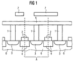
- Figure 1 shows schematically a cross section of modular Fill structures 1 to 5 of all relevant process levels up to and including the metal conductor tracks of a metallization level 5.
- the structure and structure of the modular Filling structures 1 to 5 the structure and structure of the active Areas of the chip are the same. This is the arrangement the different filling structures shown in cross section 1 to 5 largely defined.
- Extend 1 to 5 are a variety of electrical conductive contact points 1 between the metal conductor tracks the metallization level 5 and the substrate 6.
- the filling structures consist of a large number of each other same sections A. In each of sections A is an electrically conductive contact point 1 between the metal conductor tracks the metallization level 5 and the substrate 6 available.
- Each of the identical sections A comprises a proportional substrate 6 according to the size of each Section A, areas with polysilicon 2, the are above the substrate 6, a doping region 3, which in the Substrate and spaced from the regions with polysilicon 2 is arranged, and an electrically conductive contact point 1, those with the doping region 3 and the metal conductor tracks of the Metallization level 5 is electrically connected.
- the Substrate 6 are below the areas with polysilicon 2, respectively Trenches 4 filled with oxide are arranged.
- the areas with Polysilicon 2 and the trenches 4 filled with oxide adjacent Sections A of the plurality of identical sections A of the filling structures are as common areas executed.
- the substrate potential is continuously at reference potential held.
- the homogenization of the Area allocation of the chip through the applied mineral conductor tracks the metallization level 5 further improved.
- the Power supply all over the entire chip area Components applied to the substrate 6 become more homogeneous.
- the line capacities are due to a uniform substrate potential between one over the filling structures 1 to 5 located wiring level 7 and the substrate 6, the co-determining for the waveguide properties in the wiring level 7 are more uniform over the entire chip area distributed. This will improve the waveguiding properties homogenized and improved in the wiring level 7. This supports the reliable operation of the chip, because wave propagation properties of Voltage or current pulses on the chip become more predictable.
- the homogeneous substrate potential also means that Effectively suppresses the "leek-up" effect.
- FIG. 2 shows a layout structure of part of a chip area, over which fill structures extend.
- a cross section the filling structures along a line B-B is shown shown schematically in FIG. Section A from Figure 1 is indicated in Figure 2 with a dashed line.
- relevant process levels of the chip becomes a possible one Execution of a layout structure with modular filling structures shown.
- the substrate of the semiconductor chip has (not completely visible) trenches 4 filled with oxide, on which areas are applied with polysilicon 2, these only one Cover part of the surface of the trenches 4 filled with oxide.
- the trenches 4 filled with oxide and the areas deposited thereon with polysilicon 2 are contiguous throughout Areas of the chip area over which the filling structures are located extend, arranged, enclosing areas that no trenches 4 filled with oxide and areas with polysilicon 2 and arranged at regular intervals and are aligned in parallel. Within such an area, that of areas filled with polysilicon 2 and with oxide Trenches 4 is surrounded, doping regions 3 in Arranged substrate 6 of the semiconductor chip.
- band-shaped metal conductor tracks of the metallization level 5 are such arranged that each lying at right angles to each other Metal conductor tracks of the metallization level 5 crossing areas form, which are each above one of the contact points 1 and cover them.
- the metal conductor tracks of the metallization level 5 are with the contact points 1 in the area of Crossing areas electrically connected.
- the doping region 3 consists of p + -doped silicon
- the substrate 6 consists of p - -doped silicon.
- n + -doped silicon in the doping region 3 and n - -doped silicon in the substrate 6 is also possible.
Landscapes
- Internal Circuitry In Semiconductor Integrated Circuit Devices (AREA)
- Semiconductor Integrated Circuits (AREA)
Abstract
Description
- Schaffung von gleichen Schichthärten über der gesamten Chipfläche durch homogene Flächenbelegung unterhalb der jeweils obersten Schicht, wichtig hinsichtlich "CMP" (Chemical Mecnanical Polishing), "Dishing",
- Homogenisierung von Belichtungsausleuchtung und Beugungseffekten über der gesamten Chipfläche, "OPE" (Optical Proximity Effect),
- Homogenisierung und Verbesserung des Ätzprozesses über der gesamten Chipfläche, "RIE" (Reaktive Ione Etch), "Micro Loading".
- Figur 1
- einen Querschnitt von modularen Füllstrukturen bis einschließlich einer Metallisierungsebene
- Figur 2
- eine Draufsicht (Layoutstruktur) eines Teils einer Chipfläche, über die sich modulare Füllstrukturen erstrecken
Claims (7)
- Integrierter Halbleiterchip mit einem Substrat (6) und darauf angeordneten modularen Füllstrukturen (1 bis 5), die Metalleiterbahnen einer Metallisierungsebene (5) einschließen und die derart beschaffen sind, daß in den Bereichen der Chipfläche, über die sich die Füllstrukturen (1 bis 5) erstrecken, eine Vielzahl von elektrisch leitenden Kontaktstellen (1) zwischen den Metalleiterbahnen der Metallisierungsebene (5) und dem Substrat (6) vorhanden sind.
- Integrierter Halbleiterchip nach Anspruch 1,
dadurch gekennzeichnet, daß die modularen Füllstrukturen aus einer Vielzahl von untereinander gleichen Abschnitten (A) bestehen, und daß in jedem der Abschnitte (A) eine elektrisch leitende Kontaktstelle (1) zwischen den Metalleiterbahnen der Metallisierungsebene (5) und dem Substrat (6) vorhanden ist. - Integrierter Halbleiterchip nach Anspruch 2,
dadurch gekennzeichnet, daß jeder der untereinander gleichen Abschnitte (A)umfaßt.ein anteiliges Substrat (6) entsprechend der Größe des jeweiligen Abschnitts (A),Gebiete mit Polysilizium (2), die sich über dem Substrat (6) befinden,ein Dotierungsgebiet (3), das im Substrat und beabstandet von den Gebieten mit Polysilizium (2) angeordnet ist, undeine elektrisch leitende Kontaktstelle (1), die mit dem Dotierungsgebiet (3) und den Metalleiterbahnen der Metallisterungsebene (5) elektrisch leitend verbunden ist, - Integrierter Halbleiterchip nach Anspruch 3,
dadurch gekennzeichnet, daß im Substrat (6) unterhalb der Gebiete mit Polysilizium (2) jeweils mit Oxid gefüllte Gräben (4) angeordnet sind. - Integrierter Halbleiterchip nach Anspruch 3,
dadurch gekennzeichnet, daß das Dotierungsgebiet (3) und das Substrat (6) aus dotiertem Silizium gleicher Dotierungspolarität besteht, wobei das Silizium im Dotierungsgebiet (3) mit hoher Konzentration und im Substrat (6) mit niedriger Konzentration dotiert ist. - Integrierter Halbleiterchip nach Anspruch 4,
dadurch gekennzeichnet, daß die Gebiete mit Polysilizium (2) und die mit Oxid gefüllten Gräben (4) benachbarter Abschnitte (A) der Vielzahl der untereinander gleichen Abschnitte (A) der Füllstrukturen als jeweils gemeinsame Gebiete ausgeführt sind. - Integrierter Halbleiterchip nach einem der vorhergehenden Ansprüche,
dadurch gekennzeichnet, daß in den Bereichen der Chipfläche, über die sich die Füllstrukturen (1 bis 5) erstrecken, die Füllstrukturen (1 bis 5) folgende Layoutstruktur aufweisen:das Substrat (6) des Halbleiterchips weist mit Oxid gefüllte Gräben (4) auf, auf denen Gebiete mit Polysilizium (2) aufgebracht sind, wobei diese nur einen Teil der Fläche der mit Oxid gefüllten Gräben (4) bedecken,die mit Oxid gefüllten Gräben (4) und die darauf aufgebrachten Gebiete mit Polysilizium (2) sind zusammenhängend über die gesamten Bereiche der Chipfläche, über die sich die Füllstrukturen erstrecken, angeordnet, wobei sie Bereiche umschließen, die keine mit Oxid gefüllten Gräben (4) und Gebiete mit Polysilizium (2) aufweisen und die in regelmäßigen Abständen angeordnet und parallel ausgerichtet sind,innerhalb eines solchen Bereichs, der von Gebieten mit Polysilizium (2) und mit Oxid gefüllten Gräben (4) umgeben ist, sind Dotierungsgebiete (3) im Substrat (6) des Halbleiterchips angeordnet,innerhalb eines solchen Bereichs eines Dotierungsgebiets (3) sind auf das Dotierungsgebiet (3) elektrisch leitende Kontaktstellen (1) aufgebracht, die über das jeweilige Dotierungsgebiet (3) eine elektrisch leitende Kontaktierung zum Substrat (6) des Halbleiterchips herstellen, wobei sie nur einen Teil dieses Bereichs bedecken,bandförmige Metalleiterbahnen der Metallisierungsebene (5), die kreuzförmig in regelmäßigen Abständen und je Richtung parallel zueinander ausgerichtet sind, sind derart angeordnet, daß die jeweils rechtwinklig zueinander liegenden Metallleiterbahnen der Metallisierungsebene (5) Kreuzungsflächen bilden, die sich jeweils über einem der elektrisch leitenden Kontaktstellen (1) befinden und diese bedecken,die Metallleiterbahnen der Metallisierungsebene (5) sind mit den elektrisch leitenden Kontaktstellen (1) im Bereich der Kreuzungsflächen elektrisch leitend verbunden.
Applications Claiming Priority (2)
| Application Number | Priority Date | Filing Date | Title |
|---|---|---|---|
| DE19834234 | 1998-07-29 | ||
| DE19834234A DE19834234C2 (de) | 1998-07-29 | 1998-07-29 | Integrierter Halbleiterchip mit Füllstrukturen |
Publications (2)
| Publication Number | Publication Date |
|---|---|
| EP0977262A2 true EP0977262A2 (de) | 2000-02-02 |
| EP0977262A3 EP0977262A3 (de) | 2000-05-10 |
Family
ID=7875762
Family Applications (1)
| Application Number | Title | Priority Date | Filing Date |
|---|---|---|---|
| EP99112844A Withdrawn EP0977262A3 (de) | 1998-07-29 | 1999-07-02 | Integrierter Halbleiterchip mit modularen Füllstrukturen |
Country Status (6)
| Country | Link |
|---|---|
| US (1) | US6307263B1 (de) |
| EP (1) | EP0977262A3 (de) |
| JP (1) | JP4152533B2 (de) |
| KR (1) | KR100673670B1 (de) |
| DE (1) | DE19834234C2 (de) |
| TW (1) | TW447104B (de) |
Cited By (1)
| Publication number | Priority date | Publication date | Assignee | Title |
|---|---|---|---|---|
| US8765607B2 (en) | 2011-06-01 | 2014-07-01 | Freescale Semiconductor, Inc. | Active tiling placement for improved latch-up immunity |
Families Citing this family (4)
| Publication number | Priority date | Publication date | Assignee | Title |
|---|---|---|---|---|
| US6833622B1 (en) | 2003-02-27 | 2004-12-21 | Cypress Semiconductor Corp. | Semiconductor topography having an inactive region formed from a dummy structure pattern |
| DE102005008476B4 (de) | 2005-02-24 | 2006-12-21 | Infineon Technologies Ag | Leitbahnanordnung sowie zugehöriges Herstellungsverfahren |
| KR100855558B1 (ko) * | 2007-07-02 | 2008-09-01 | 삼성전자주식회사 | 반도체 집적 회로 장치 및 그 제조 방법 |
| JP5475260B2 (ja) | 2008-04-18 | 2014-04-16 | 株式会社神戸製鋼所 | 配線構造、薄膜トランジスタ基板およびその製造方法、並びに表示装置 |
Family Cites Families (10)
| Publication number | Priority date | Publication date | Assignee | Title |
|---|---|---|---|---|
| JPS6370550A (ja) * | 1986-09-12 | 1988-03-30 | Nec Corp | 半導体集積回路装置 |
| JP2858404B2 (ja) * | 1990-06-08 | 1999-02-17 | 株式会社デンソー | 絶縁ゲート型バイポーラトランジスタおよびその製造方法 |
| US5196920A (en) * | 1992-04-21 | 1993-03-23 | Mitsubishi Denki Kabushiki Kaisha | Semiconductor integrated circuit device for limiting capacitive coupling between adjacent circuit blocks |
| US5625232A (en) * | 1994-07-15 | 1997-04-29 | Texas Instruments Incorporated | Reliability of metal leads in high speed LSI semiconductors using dummy vias |
| US5464996A (en) * | 1994-08-29 | 1995-11-07 | Texas Instruments Incorporated | Process tracking bias generator for advanced lateral overflow antiblooming drain |
| JP3207347B2 (ja) * | 1996-01-26 | 2001-09-10 | シャープ株式会社 | 半導体装置 |
| US5747380A (en) * | 1996-02-26 | 1998-05-05 | Taiwan Semiconductor Manufacturing Company, Ltd. | Robust end-point detection for contact and via etching |
| EP0888636A1 (de) * | 1996-03-22 | 1999-01-07 | Telefonaktiebolaget Lm Ericsson | Durch ein gitter von elektrisch leitenden stiften abgeschirmte halbleiteranordnung und verfahren dafür |
| TW329563B (en) * | 1996-06-01 | 1998-04-11 | Winbond Electronics Corp | The manufacturing method for load resistors of SRAM |
| JPH1041302A (ja) * | 1996-07-26 | 1998-02-13 | Nec Corp | 半導体装置およびその製造方法 |
-
1998
- 1998-07-29 DE DE19834234A patent/DE19834234C2/de not_active Expired - Fee Related
-
1999
- 1999-07-02 EP EP99112844A patent/EP0977262A3/de not_active Withdrawn
- 1999-07-14 TW TW088111925A patent/TW447104B/zh not_active IP Right Cessation
- 1999-07-26 JP JP21085599A patent/JP4152533B2/ja not_active Expired - Fee Related
- 1999-07-28 KR KR1019990030757A patent/KR100673670B1/ko not_active Expired - Fee Related
- 1999-07-29 US US09/363,263 patent/US6307263B1/en not_active Expired - Lifetime
Cited By (1)
| Publication number | Priority date | Publication date | Assignee | Title |
|---|---|---|---|---|
| US8765607B2 (en) | 2011-06-01 | 2014-07-01 | Freescale Semiconductor, Inc. | Active tiling placement for improved latch-up immunity |
Also Published As
| Publication number | Publication date |
|---|---|
| TW447104B (en) | 2001-07-21 |
| KR100673670B1 (ko) | 2007-01-23 |
| KR20000012029A (ko) | 2000-02-25 |
| DE19834234C2 (de) | 2000-11-30 |
| US6307263B1 (en) | 2001-10-23 |
| JP2000058766A (ja) | 2000-02-25 |
| EP0977262A3 (de) | 2000-05-10 |
| DE19834234A1 (de) | 2000-02-10 |
| JP4152533B2 (ja) | 2008-09-17 |
Similar Documents
| Publication | Publication Date | Title |
|---|---|---|
| DE19624916C2 (de) | Flüssigkristallanzeigevorrichtung und Verfahren zu ihrer Herstellung | |
| DE69031603T2 (de) | Integrierter Torschaltungs-Schaltkreis | |
| CH699933A1 (de) | Vertikaler Hallsensor. | |
| DE3423211C2 (de) | Halbleiterbauteil | |
| DE10353387A1 (de) | Leistungstransistoranordnung und Verfahren zu deren Herstellung | |
| DE102008020452B4 (de) | Halbleiterschaltung mit einer Matching-Struktur und Verfahren zur Erzeugung eines Layouts einer Halbleiterschaltung mit einer Matching-Struktur | |
| DE69622115T2 (de) | Verbesserungen an nichtflüchtigen Speicheranordnungen oder bezüglich derselben | |
| DE4444584A1 (de) | Halbleiterwafer | |
| DE10164606B4 (de) | Flip-Chip-Halbleitereinrichtung mit außerhalb von Energiezufuhranschlussflächen angeordneten Signalanschlussflächen | |
| DE102005059035B4 (de) | Isolationsgrabenstrukturen für hohe Spannungen | |
| EP0362493A1 (de) | Hallelement | |
| DE19834234C2 (de) | Integrierter Halbleiterchip mit Füllstrukturen | |
| DE1616438C3 (de) | Integrierte Schaltung, Verwendung dieser Schaltung und Verfahren zu ihrer Herstellung | |
| DE69033641T2 (de) | Stromversorgungssystem für Master slice integrierte Schaltung | |
| DE4127795A1 (de) | Herstellungsverfahren und aufbau eines mos-transistors | |
| DE2353770A1 (de) | Halbleiteranordnung | |
| DE2342923B1 (de) | Verfahren zur Herstellung einer Zweiphasen-Ladungsverschiebeanordnung und nach diesem Verfahren hergestellte Zweiphasen-Ladungsverschiebeanordnung | |
| DE102004060369A1 (de) | Halbleiterscheibe mit Teststruktur | |
| DE2540350A1 (de) | Halbleiter-bauelement | |
| WO2001037376A1 (de) | Anordnung zur elektrischen verbindung zwischen chips in einer dreidimensional ausgeführten schaltung | |
| DE68925150T2 (de) | Bipolartransistor und Verfahren zu dessen Herstellung | |
| DE19918671A1 (de) | Vertikal integrierbare Schaltung und Verfahren zu ihrer Herstellung | |
| DE2213657C3 (de) | Planare integrierte Halbleiterschaltung | |
| DE102005002678A1 (de) | Ritzrahmen mit verbesserter Füllroutine | |
| DE19960563B4 (de) | Halbleiterstruktur und entsprechendes Herstellungsverfahren |
Legal Events
| Date | Code | Title | Description |
|---|---|---|---|
| PUAI | Public reference made under article 153(3) epc to a published international application that has entered the european phase |
Free format text: ORIGINAL CODE: 0009012 |
|
| AK | Designated contracting states |
Kind code of ref document: A2 Designated state(s): DE FR GB IE IT |
|
| AX | Request for extension of the european patent |
Free format text: AL;LT;LV;MK;RO;SI |
|
| PUAL | Search report despatched |
Free format text: ORIGINAL CODE: 0009013 |
|
| AK | Designated contracting states |
Kind code of ref document: A3 Designated state(s): AT BE CH CY DE DK ES FI FR GB GR IE IT LI LU MC NL PT SE |
|
| AX | Request for extension of the european patent |
Free format text: AL;LT;LV;MK;RO;SI |
|
| RIC1 | Information provided on ipc code assigned before grant |
Free format text: 7H 01L 23/52 A, 7H 01L 23/528 B, 7H 01L 23/58 B |
|
| 17P | Request for examination filed |
Effective date: 20000818 |
|
| AKX | Designation fees paid |
Free format text: DE FR GB IE IT |
|
| RAP1 | Party data changed (applicant data changed or rights of an application transferred) |
Owner name: INFINEON TECHNOLOGIES AG |
|
| STAA | Information on the status of an ep patent application or granted ep patent |
Free format text: STATUS: THE APPLICATION HAS BEEN WITHDRAWN |
|
| 18W | Application withdrawn |
Effective date: 20060329 |