EP0977262A2 - Integrated semiconductor chip with modular dummy structures - Google Patents
Integrated semiconductor chip with modular dummy structures Download PDFInfo
- Publication number
- EP0977262A2 EP0977262A2 EP99112844A EP99112844A EP0977262A2 EP 0977262 A2 EP0977262 A2 EP 0977262A2 EP 99112844 A EP99112844 A EP 99112844A EP 99112844 A EP99112844 A EP 99112844A EP 0977262 A2 EP0977262 A2 EP 0977262A2
- Authority
- EP
- European Patent Office
- Prior art keywords
- substrate
- areas
- semiconductor chip
- polysilicon
- filling structures
- Prior art date
- Legal status (The legal status is an assumption and is not a legal conclusion. Google has not performed a legal analysis and makes no representation as to the accuracy of the status listed.)
- Withdrawn
Links
Images

Classifications
-
- H—ELECTRICITY
- H01—ELECTRIC ELEMENTS
- H01L—SEMICONDUCTOR DEVICES NOT COVERED BY CLASS H10
- H01L27/00—Devices consisting of a plurality of semiconductor or other solid-state components formed in or on a common substrate
- H01L27/02—Devices consisting of a plurality of semiconductor or other solid-state components formed in or on a common substrate including semiconductor components specially adapted for rectifying, oscillating, amplifying or switching and having at least one potential-jump barrier or surface barrier; including integrated passive circuit elements with at least one potential-jump barrier or surface barrier
- H01L27/04—Devices consisting of a plurality of semiconductor or other solid-state components formed in or on a common substrate including semiconductor components specially adapted for rectifying, oscillating, amplifying or switching and having at least one potential-jump barrier or surface barrier; including integrated passive circuit elements with at least one potential-jump barrier or surface barrier the substrate being a semiconductor body
-
- H—ELECTRICITY
- H01—ELECTRIC ELEMENTS
- H01L—SEMICONDUCTOR DEVICES NOT COVERED BY CLASS H10
- H01L23/00—Details of semiconductor or other solid state devices
- H01L23/48—Arrangements for conducting electric current to or from the solid state body in operation, e.g. leads, terminal arrangements ; Selection of materials therefor
- H01L23/482—Arrangements for conducting electric current to or from the solid state body in operation, e.g. leads, terminal arrangements ; Selection of materials therefor consisting of lead-in layers inseparably applied to the semiconductor body
- H01L23/485—Arrangements for conducting electric current to or from the solid state body in operation, e.g. leads, terminal arrangements ; Selection of materials therefor consisting of lead-in layers inseparably applied to the semiconductor body consisting of layered constructions comprising conductive layers and insulating layers, e.g. planar contacts
-
- H—ELECTRICITY
- H01—ELECTRIC ELEMENTS
- H01L—SEMICONDUCTOR DEVICES NOT COVERED BY CLASS H10
- H01L2924/00—Indexing scheme for arrangements or methods for connecting or disconnecting semiconductor or solid-state bodies as covered by H01L24/00
- H01L2924/0001—Technical content checked by a classifier
- H01L2924/0002—Not covered by any one of groups H01L24/00, H01L24/00 and H01L2224/00
Abstract
Description
Die vorliegende Erfindung betrifft einen integrierten Halbleiterchip
nach dem Oberbegriff des Patentanspruchs 1.The present invention relates to an integrated semiconductor chip
according to the preamble of
Betrachtet man die Fläche (Layoutstruktur) eines integrierten Halbleiterchips, lassen sich aufgrund der Strukturunterschiede in der obersten Schicht im allgemeinen sogenannte aktive Bereiche und inaktive Bereiche erkennen. In den aktiven Bereichen sind beispielsweise Bauelemente oder Funktionsgruppen (z.B. Transistoren, Speicherzellen) angeordnet, die die Funktionalität des Halbleiterchips bewerkstelligen, in den inaktiven Bereichen sind hingegen keine Bauelemente oder Funktionsgruppen enthalten. Moderne Fertigungsprozesse erfordern hinsichtlich des topographischen Aufbaus von integrierten Halbleiterchips insbesondere eine homogene Flächenbelegung in allen relevanten Prozeßebenen vom Substrat bis einschließlich einer ersten Metallisierungsebene. Das bedeutet, daß der strukturelle Aufbau dieser Prozeßebenen in den aktiven und inaktiven Bereichen des Chips weitgehend ähnlich sein soll. Zu diesem Zweck werden innerhalb der inaktiven Bereiche in den oben genannten Prozeßebenen sogenannte modulare Füllstrukturen vorgesehen, die ähnlich aufgebaut sind, wie die Strukturen der aktiven Bereiche. Die Verwendung von modularen Füllstrukturen ist bereits gängige Praxis. Sie werden, nochmals kurz in Schlagworten dargestellt, vor allem aus drei Gründen verwendet:
- Schaffung von gleichen Schichthärten über der gesamten Chipfläche durch homogene Flächenbelegung unterhalb der jeweils obersten Schicht, wichtig hinsichtlich "CMP" (Chemical Mecnanical Polishing), "Dishing",
- Homogenisierung von Belichtungsausleuchtung und Beugungseffekten über der gesamten Chipfläche, "OPE" (Optical Proximity Effect),
- Homogenisierung und Verbesserung des Ätzprozesses über der gesamten Chipfläche, "RIE" (Reaktive Ione Etch), "Micro Loading".
- Creation of the same layer hardness over the entire chip area through homogeneous area coverage below the top layer, important with regard to "CMP" (Chemical Mecnanical Polishing), "Dishing",
- Homogenization of exposure illumination and diffraction effects over the entire chip area, "OPE" (Optical Proximity Effect),
- Homogenization and improvement of the etching process over the entire chip area, "RIE" (reactive ion etch), "micro loading".
Für den Betrieb des Halbleiterchips ist es erstrebenswert, das Substratpotential des Chips bestmöglich zu homogenisieren. Dadurch wird erreicht, daß das Substratpotential für alle Bauelemente, die auf dem Substrat aufgebracht sind, gleichmäßig verteilt ist. Daraus ergibt sich eine bessere und gleichmäßigere Spannungsversorgung aller über die Chipfläche verteilten Bauelemente. Die Wellenausbreitungseigenschaften von Spannungsimpulsen auf elektrischen Leitern sind über einheitlichem Potential berechenbarer und homogener. Durch ein einheitliches Substratpotential werden deshalb auch die Wellenleitungseigenschaften von darüber liegenden Verdrahtungsebenen verbessert. Bisher wurde versucht, eine Homogenisierung des elektrischen Substratpotentials durch Verwendung von EPI-Substraten und durch zusätzliche Substratkontakte in den einzelnen Schaltungen zu erreichen. Durch Verwendung von EPI-Substraten kann außerdem der bekannte "Latch-up"-Effekt verkleinert werden. Ein Nachteil dieses Vorgehens ist, daß zur Aufbringung der Epitaxie-Schicht auf das Substrat ein zusätzlicher kostspieliger Prozeßschritt beim Herstellungsprozeß notwendig ist.For the operation of the semiconductor chip, it is desirable to homogenize the substrate potential of the chip as best as possible. This ensures that the substrate potential for everyone Components that are applied to the substrate, is evenly distributed. This results in a better and more uniform power supply for all over the chip area distributed components. The wave propagation properties of voltage pulses on electrical conductors are about uniform More predictable and more homogeneous. Through a The waveguide properties are therefore also a uniform substrate potential from wiring levels above improved. So far, attempts have been made to homogenize it the electrical substrate potential by use of EPI substrates and through additional substrate contacts in to reach the individual circuits. By using EPI substrates can also have the well-known "latch-up" effect be made smaller. A disadvantage of this approach is that an additional one to apply the epitaxial layer to the substrate costly process step in the manufacturing process necessary is.
Die Aufgabe der vorliegenden Erfindung ist es, eine flächendeckende Homogenisierung der Substratpotentialverhältnisse auf einem integrierten Halbleiterchip zu erreichen. Dabei soll der entsprechende Aufwand beim Herstellungsprozeß des Chips möglichst gering gehalten werden. The object of the present invention is to provide a comprehensive coverage Homogenization of the substrate potential relationships to achieve on an integrated semiconductor chip. Here the corresponding effort in the manufacturing process of Chips are kept as low as possible.
Die Aufgabe wird gelöst durch einen integrierten Halbleiterchip
mit modularen Füllstrukturen nach den Merkmalen des Patentanspruchs
1.The task is solved by an integrated semiconductor chip
with modular filling structures according to the features of the
Vorteilhafte Aus- und Weiterbildungen sind in Unteransprüchen gekennzeichnet.Advantageous training and further education are in the subclaims featured.
Im folgenden wird die Erfindung anhand der in der Zeichnung dargestellten Figuren näher erläutert.In the following the invention based on the in the drawing illustrated figures explained in more detail.
Es zeigen:
Figur 1- einen Querschnitt von modularen Füllstrukturen bis einschließlich einer Metallisierungsebene
Figur 2- eine Draufsicht (Layoutstruktur) eines Teils einer Chipfläche, über die sich modulare Füllstrukturen erstrecken
- Figure 1
- a cross section of modular filling structures up to and including a metallization level
- Figure 2
- a plan view (layout structure) of part of a chip area over which modular fill structures extend
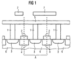
Figur 1 zeigt schematisch einen Querschnitt von modularen
Füllstrukturen 1 bis 5 aller relevanten Prozeßebenen bis einschließlich
den Metalleiterbahnen einer Metallisierungsebene
5. Um die eingangs genannten Aufgaben möglichst gut erfüllen
zu können, sollte der Aufbau und die Struktur der modularen
Füllstrukturen 1 bis 5 dem Aufbau und der Struktur der aktiven
Bereiche des Chips gleichen. Dadurch ist die Anordnung
der im Querschnitt dargestellten unterschiedlichen Füllstrukturen
1 bis 5 weitgehend festgelegt.Figure 1 shows schematically a cross section of
In den Bereichen der Chipfläche, über die sich modulare Füllstrukturen
1 bis 5 erstrecken, sind eine Vielzahl von elektrisch
leitenden Kontaktstellen 1 zwischen den Metalleiterbahnen
der Metallisierungsebene 5 una dem Substrat 6 angeordnet.
Die Füllstrukturen bestehen aus einer Vielzahl von untereinander
gleichen Abschnitten A. In jedem der Abschnitte A
ist eine elektrisch leitende Kontaktstelle 1 zwischen den Metalleiterbahnen
der Metallisierungsebene 5 und dem Substrat 6
vorhanden. Jeder der untereinander gleichen Abschnitte A umfaßt
ein anteiliges Substrat 6 entsprechend der Größe des jeweiligen
Abschnitts A, Gebiete mit Polysilizium 2, die sich
über dem Substrat 6 befinden, ein Dotierungsgebiet 3, das im
Substrat und beabstandet von den Gebieten mit Polysilizium 2
angeordnet ist, und eine elektrisch leitende Kontaktstelle 1,
die mit dem Dotierungsgebiet 3 und den Metalleiterbahnen der
Metallisierungsebene 5 elektrisch leitend verbunden ist. Im
Substrat 6 sind unterhalb der Gebiete mit Polysilizium 2 jeweils
mit Oxid gefüllte Gräben 4 angeordnet. Die Gebiete mit
Polysilizium 2 und die mit Oxid gefüllten Gräben 4 benachbarter
Abschnitte A der Vielzahl der untereinander gleichen Abschnitte
A der Füllstrukturen sind als jeweils gemeinsame Gebiete
ausgeführt.In the areas of the chip area over which there are modular filling structures
Extend 1 to 5 are a variety of electrical
Bisher wurden Füllstrukturen zur Homogenisierung der Flächenbelegung
eines Chips elektrisch nicht benutzt. Daher bestanden
auch in den Bereichen einer Chipfläche, über die sich
Füllstrukturen erstrecken, keine elektrisch leitenden Verbindungen
zwischen dem Substrat 6 und darüber befindlichen Prozeßebenen.
In den Bereichen der Chipfläche, über die sich modulare
Füllstrukturen erstrecken, sind Metalleiterbahnen der
Metallisierungsebene 5 aufgebracht. Um das Substratpotential
des Chips zu homogenisieren, sind diese über elektrisch leitende
Kontaktstellen 1 und Dotierungsgebiete 3 mit dem
Substrat 6 elektrisch leitend verbunden. Die Dotierungsgebiete
3 umfassen dabei Gebiete mit hochdotiertem Silizium. Die
Metalleiterbahnen der Metallisierungsebene 5 sind im Betrieb
des Halbleiterchips ihrerseits auf Bezugspotential (beispielsweise
"GND")So far, filling structures have been used to homogenize the area coverage
of a chip is not used electrically. Therefore passed
also in the areas of a chip area over which
Filling structures extend, no electrically conductive connections
between the
Durch die flächendeckende elektrisch leitende Verbindung zwischen
den Metalleiterbahnen der Metallisierungsebene 5 und
dem Substrat 6 wird das Substratpotential durchgehend auf Bezugspotential
gehalten. Daneben wird die Homogenisierung der
Flächenbelegung des Chips durch die aufgebrachten Meralleiterbahnen
der Metallisierungsebene 5 weiter verbessert. Die
Spannungsversorgung aller über der gesamten Chipfläche auf
dem Substrat 6 aufgebrachten Bauelemente wird homogener.
Durch ein einheitliches Substratpotential sind die Leitungskapazitäten
zwischen einer über den Füllstrukturen 1 bis 5
befindlichen Verdrahtungsebene 7 und dem Substrat 6, die mitbestimmend
für die Wellenleitungseigenschaften in der Verdrahtungsebene
7 sind, über die gesamte Chipfläche gleichmäßiger
verteilt. Dadurch werden die Wellenleitungseigenschaften
in der Verdrahtungsebene 7 homogenisiert und verbessert.
Dies wirkt unterstützend hinsichtlich eines zuverlässigen Betriebs
des Chips, da Wellenausbreitungseigenschaften von
Spannungs- oder Stromimpulsen auf dem Chip berechenbarer werden.
Durch homogenes Substratpotential wird außerdem der
"Lauch-up"-Effekt wirksam unterdrückt.Due to the area-wide electrically conductive connection between
the metal conductor tracks of the
Durch eine derartige Anordnung ist für eine Homogenisierung
des Substratpotentials weder eine zusätzliche Chipfläche noch
ein zusätzlicher Prozeßschritt notwendig. Es wird keine zusätzliche
Chipfläche benötigt, da die modularen Füllstrukturen
1 bis 5, die, wie oben dargestellt, bereits zur Homogenisierung
der Flächenbelegung verwendet werden, nur eine weitere
Funktion erhalten, indem sie nun auch für elektrische
Zwecke benutzt werden. Es erfordert keinen zusätzlichen Prozeßschritt,
da bisher vorgesehene Füllmuster nunmehr in Form
der Kontaktstellen 1 elektrisch leitend sind, in ihrer geometrischen
Form und Anordnung jedoch gleich bleiben. Elektrische
Kontakte sind notwendig in den aktiven Bereichen des
Chips, beispielsweise zur Kontaktierung von Bauelementen, so
daß der dazu notwendige Prozeßschritt lediglich auf die Flächen
des Chips ausgedehnt wird, über die sich Füllstrukturen
1 bis 5 erstrecken. Die elektrisch leitenden Kontaktstellen 1
entsprechen in ihrem Aufbau dabei den Kontakten in den aktiven
Bereichen des Chips. Der Prozeßschritt zur Anordnung der
Metalleiterbahnen der Metallisierungsebene 5 entspricht dem
Prozeßschritt, in dem die Merallisierungsschicht in den aktiven
Bereichen des Chips aufgebracht wird. Such an arrangement is for homogenization
the substrate potential neither an additional chip area nor
an additional process step is necessary. There will be no additional
Chip area is required because of the
Figur 2 zeigt eine Layoutstruktur eines Teils einer Chipfläche, über die sich Füllstrukturen erstrecken. Ein Querschnitt der Füllstrukturen entlang einer Linie B-B ist in der Darstellung nach Figur 1 schematisch gezeigt. Ein Abschnitt A aus Figur 1 ist in Figur 2 mit einer gestrichelten Linie gekennzeichnet. Anhand der in Figur 1 im Querschnitt dargestellten relevanten Prozeßebenen des Chips wird eine mögliche Ausführung einer Layoutstruktur mit modularen Füllstrukturen dargestellt.FIG. 2 shows a layout structure of part of a chip area, over which fill structures extend. A cross section the filling structures along a line B-B is shown shown schematically in FIG. Section A from Figure 1 is indicated in Figure 2 with a dashed line. Using the cross-section shown in Figure 1 relevant process levels of the chip becomes a possible one Execution of a layout structure with modular filling structures shown.
Das Substrat des Halbleiterchips weist (nicht vollständig
sichtbare) mit Oxid gefüllte Gräben 4 auf, auf denen Gebiete
mit Polysilizium 2 aufgebracht sind, wobei diese nur einen
Teil der Fläche der mit Oxid gefüllten Gräben 4 bedecken. Die
mit Oxid gefüllten Gräben 4 und die darauf aufgebrachten Gebiete
mit Polysilizium 2 sind zusammenhängend über die gesamten
Bereiche der Chipfläche, über die sich die Füllstrukturen
erstrecken, angeordnet, wobei sie Bereiche umschließen, die
keine mit Oxid gefüllten Gräben 4 und Gebiete mit Polysilizium
2 aufweisen und die in regelmäßigen Abständen angeordnet
und parallel ausgerichtet sind. Innerhalb eines solchen Bereichs,
der von Gebieten mit Polysilizium 2 und mit Oxid gefüllten
Gräben 4 umgeben ist, sind Dotierungsgebiete 3 im
Substrat 6 des Halbleiterchips angeordnet. Innerhalb eines
solchen Bereichs eines Dotierungsgebiets 3 sind auf das Dotierungsgebiet
3 elektrisch leitende Kontaktstellen 1 aufgebracht,
die über das jeweilige Dotierungsgebiet 3 eine elektrisch
leitende Kontaktierung zum Substrat 6 des Halbleiterchips
herstellen, wobei sie nur einen Teil dieses Bereichs
bedecken. Bandförmige Metalleiterbahnen der Metallisierungsebene
5, die kreuzförmig in regelmäßigen Abständen und je
Richtung parallel zueinander ausgerichtet sind, sind derart
angeordnet, daß die jeweils rechtwinklig zueinander liegenden
Metalleiterbahnen der Metallisierungsebene 5 Kreuzungsflächen
bilden, die sich jeweils über einem der Kontaktestellen 1 befinden
und diese bedecken. Die Metalleiterbahen der Metallisierungsebene
5 sind mit den Kontaktstellen 1 im Bereich der
Kreuzungsflächen elektrisch leitend verbunden.The substrate of the semiconductor chip has (not completely
visible) trenches 4 filled with oxide, on which areas
are applied with
Im Ausführungsbeispiel besteht das Dotierungsgebiet 3 aus p+-dotiertem
Silizium, das Substrat 6 aus p--dotiertem Silizium.
Es ist jedoch auch eine Ausführung mit n+-dotiertem Silizium
im Dotierungsgebiet 3 und n--dotiertem Silizium im Substrat 6
möglich.In the exemplary embodiment, the
Claims (7)
dadurch gekennzeichnet, daß die modularen Füllstrukturen aus einer Vielzahl von untereinander gleichen Abschnitten (A) bestehen, und daß in jedem der Abschnitte (A) eine elektrisch leitende Kontaktstelle (1) zwischen den Metalleiterbahnen der Metallisierungsebene (5) und dem Substrat (6) vorhanden ist.Integrated semiconductor chip according to Claim 1,
characterized in that the modular filling structures consist of a plurality of mutually identical sections (A) and in that in each of the sections (A) there is an electrically conductive contact point (1) between the metal conductor tracks of the metallization level (5) and the substrate (6) is.
dadurch gekennzeichnet, daß jeder der untereinander gleichen Abschnitte (A)
characterized in that each of the mutually identical sections (A)
dadurch gekennzeichnet, daß im Substrat (6) unterhalb der Gebiete mit Polysilizium (2) jeweils mit Oxid gefüllte Gräben (4) angeordnet sind.Integrated semiconductor chip according to Claim 3,
characterized in that trenches (4) filled with oxide are arranged in the substrate (6) below the regions with polysilicon (2).
dadurch gekennzeichnet, daß das Dotierungsgebiet (3) und das Substrat (6) aus dotiertem Silizium gleicher Dotierungspolarität besteht, wobei das Silizium im Dotierungsgebiet (3) mit hoher Konzentration und im Substrat (6) mit niedriger Konzentration dotiert ist.Integrated semiconductor chip according to Claim 3,
characterized in that the doping region (3) and the substrate (6) consist of doped silicon of the same doping polarity, the silicon being doped in the doping region (3) with a high concentration and in the substrate (6) with a low concentration.
dadurch gekennzeichnet, daß die Gebiete mit Polysilizium (2) und die mit Oxid gefüllten Gräben (4) benachbarter Abschnitte (A) der Vielzahl der untereinander gleichen Abschnitte (A) der Füllstrukturen als jeweils gemeinsame Gebiete ausgeführt sind.Integrated semiconductor chip according to Claim 4,
characterized in that the areas with polysilicon (2) and the trenches (4) filled with oxide (4) of adjacent sections (A) of the plurality of sections (A) of the filling structures which are identical to one another are each designed as common areas.
dadurch gekennzeichnet, daß in den Bereichen der Chipfläche, über die sich die Füllstrukturen (1 bis 5) erstrecken, die Füllstrukturen (1 bis 5) folgende Layoutstruktur aufweisen:
characterized in that in the areas of the chip area over which the filling structures (1 to 5) extend, the filling structures (1 to 5) have the following layout structure:
Applications Claiming Priority (2)
| Application Number | Priority Date | Filing Date | Title |
|---|---|---|---|
| DE19834234 | 1998-07-29 | ||
| DE19834234A DE19834234C2 (en) | 1998-07-29 | 1998-07-29 | Integrated semiconductor chip with filling structures |
Publications (2)
| Publication Number | Publication Date |
|---|---|
| EP0977262A2 true EP0977262A2 (en) | 2000-02-02 |
| EP0977262A3 EP0977262A3 (en) | 2000-05-10 |
Family
ID=7875762
Family Applications (1)
| Application Number | Title | Priority Date | Filing Date |
|---|---|---|---|
| EP99112844A Withdrawn EP0977262A3 (en) | 1998-07-29 | 1999-07-02 | Integrated semiconductor chip with modular dummy structures |
Country Status (6)
| Country | Link |
|---|---|
| US (1) | US6307263B1 (en) |
| EP (1) | EP0977262A3 (en) |
| JP (1) | JP4152533B2 (en) |
| KR (1) | KR100673670B1 (en) |
| DE (1) | DE19834234C2 (en) |
| TW (1) | TW447104B (en) |
Cited By (1)
| Publication number | Priority date | Publication date | Assignee | Title |
|---|---|---|---|---|
| US8765607B2 (en) | 2011-06-01 | 2014-07-01 | Freescale Semiconductor, Inc. | Active tiling placement for improved latch-up immunity |
Families Citing this family (3)
| Publication number | Priority date | Publication date | Assignee | Title |
|---|---|---|---|---|
| US6833622B1 (en) | 2003-02-27 | 2004-12-21 | Cypress Semiconductor Corp. | Semiconductor topography having an inactive region formed from a dummy structure pattern |
| DE102005008476B4 (en) * | 2005-02-24 | 2006-12-21 | Infineon Technologies Ag | Guideway arrangement and associated production method |
| KR100855558B1 (en) | 2007-07-02 | 2008-09-01 | 삼성전자주식회사 | Semiconductor integrated circuit device and method of fabricating the same |
Citations (4)
| Publication number | Priority date | Publication date | Assignee | Title |
|---|---|---|---|---|
| US4937649A (en) * | 1986-09-12 | 1990-06-26 | Nec Corporation | Semiconductor integrated circuit having a capacitor for stabilizing a voltage at a power supplying wiring |
| EP0567694A1 (en) * | 1992-04-21 | 1993-11-03 | Mitsubishi Denki Kabushiki Kaisha | Semiconductor integrated circuit device with noise protecting shield |
| US5464992A (en) * | 1990-06-08 | 1995-11-07 | Nippondenso Co., Ltd. | Insulated gate bipolar transistor provided with a minority carrier extracting layer |
| WO1997035344A1 (en) * | 1996-03-22 | 1997-09-25 | Telefonaktiebolaget Lm Ericsson | Semiconductor device shielded by an array of electrically conducting pins and a method to manufacture such a device |
Family Cites Families (6)
| Publication number | Priority date | Publication date | Assignee | Title |
|---|---|---|---|---|
| US5625232A (en) * | 1994-07-15 | 1997-04-29 | Texas Instruments Incorporated | Reliability of metal leads in high speed LSI semiconductors using dummy vias |
| US5464996A (en) * | 1994-08-29 | 1995-11-07 | Texas Instruments Incorporated | Process tracking bias generator for advanced lateral overflow antiblooming drain |
| JP3207347B2 (en) * | 1996-01-26 | 2001-09-10 | シャープ株式会社 | Semiconductor device |
| US5747380A (en) * | 1996-02-26 | 1998-05-05 | Taiwan Semiconductor Manufacturing Company, Ltd. | Robust end-point detection for contact and via etching |
| TW329563B (en) * | 1996-06-01 | 1998-04-11 | Winbond Electronics Corp | The manufacturing method for load resistors of SRAM |
| JPH1041302A (en) * | 1996-07-26 | 1998-02-13 | Nec Corp | Semiconductor device and its manufacture |
-
1998
- 1998-07-29 DE DE19834234A patent/DE19834234C2/en not_active Expired - Fee Related
-
1999
- 1999-07-02 EP EP99112844A patent/EP0977262A3/en not_active Withdrawn
- 1999-07-14 TW TW088111925A patent/TW447104B/en not_active IP Right Cessation
- 1999-07-26 JP JP21085599A patent/JP4152533B2/en not_active Expired - Fee Related
- 1999-07-28 KR KR1019990030757A patent/KR100673670B1/en not_active IP Right Cessation
- 1999-07-29 US US09/363,263 patent/US6307263B1/en not_active Expired - Lifetime
Patent Citations (4)
| Publication number | Priority date | Publication date | Assignee | Title |
|---|---|---|---|---|
| US4937649A (en) * | 1986-09-12 | 1990-06-26 | Nec Corporation | Semiconductor integrated circuit having a capacitor for stabilizing a voltage at a power supplying wiring |
| US5464992A (en) * | 1990-06-08 | 1995-11-07 | Nippondenso Co., Ltd. | Insulated gate bipolar transistor provided with a minority carrier extracting layer |
| EP0567694A1 (en) * | 1992-04-21 | 1993-11-03 | Mitsubishi Denki Kabushiki Kaisha | Semiconductor integrated circuit device with noise protecting shield |
| WO1997035344A1 (en) * | 1996-03-22 | 1997-09-25 | Telefonaktiebolaget Lm Ericsson | Semiconductor device shielded by an array of electrically conducting pins and a method to manufacture such a device |
Cited By (1)
| Publication number | Priority date | Publication date | Assignee | Title |
|---|---|---|---|---|
| US8765607B2 (en) | 2011-06-01 | 2014-07-01 | Freescale Semiconductor, Inc. | Active tiling placement for improved latch-up immunity |
Also Published As
| Publication number | Publication date |
|---|---|
| KR20000012029A (en) | 2000-02-25 |
| DE19834234A1 (en) | 2000-02-10 |
| JP4152533B2 (en) | 2008-09-17 |
| TW447104B (en) | 2001-07-21 |
| JP2000058766A (en) | 2000-02-25 |
| DE19834234C2 (en) | 2000-11-30 |
| KR100673670B1 (en) | 2007-01-23 |
| EP0977262A3 (en) | 2000-05-10 |
| US6307263B1 (en) | 2001-10-23 |
Similar Documents
| Publication | Publication Date | Title |
|---|---|---|
| DE19624916C2 (en) | Liquid crystal display device and method of manufacturing the same | |
| DE3423211C2 (en) | Semiconductor device | |
| DE102005059035B4 (en) | Isolation trench structures for high voltages | |
| DE1514818A1 (en) | Solid-state circuit, consisting of a semiconductor body with inserted active components and an insulating layer with applied passive components and conductor tracks | |
| DE2351761A1 (en) | MONOLITHICALLY INTEGRATED SEMI-CONDUCTOR CIRCUIT ARRANGEMENT DIVIDED INTO CHIPS | |
| DE2334405B2 (en) | Large-scale integrated (LSI) semiconductor circuit and method for manufacturing a large number of such semiconductor circuits | |
| DE4444584A1 (en) | Semiconductor wafer for burn-in testing of integrated circuits | |
| DE10164606B4 (en) | A flip-chip semiconductor device with signal pads arranged outside power supply pads | |
| DE102008020452B4 (en) | A semiconductor circuit with a matching structure and a method for generating a layout of a semiconductor circuit with a matching structure | |
| DE102006008454B4 (en) | Pad structure, pad layout structure, semiconductor device, and pad layout method | |
| DE2514012B1 (en) | MONOLITHICALLY INTEGRATED SEMI-CONDUCTOR CIRCUIT, IN PARTICULAR FOR COUPLING COMPONENTS OF SWITCHING SYSTEMS | |
| DE1616438C3 (en) | Integrated circuit, use of this circuit and method of making it | |
| DE19834234C2 (en) | Integrated semiconductor chip with filling structures | |
| DE4127795A1 (en) | MANUFACTURING METHOD AND DESIGN OF A MOS TRANSISTOR | |
| WO2001037376A1 (en) | Arrangement for electrically connecting chips in a circuit that is embodied in a three-dimensional manner | |
| DE4327290C2 (en) | Integrated semiconductor circuit | |
| DE2540350A1 (en) | SEMICONDUCTOR COMPONENT | |
| DE102004060369A1 (en) | Semiconductor circuit manufacturing wafer, has connection contacts provided in test structure-area and forming two rows, which run in longitudinal direction and are displaced against each other transverse to longitudinal direction | |
| EP1075027A2 (en) | Contacting of metal interconnections of integrated semiconductor chips | |
| DE2213657C3 (en) | Planar semiconductor integrated circuit | |
| DE19918671A1 (en) | Vertically integrable circuit and method for its manufacture | |
| DE10127350C1 (en) | Semiconductor structure with buried conductor tracks and method for electrical contacting of the buried conductor tracks | |
| DE10259634A1 (en) | Process for making contacts on a wafer | |
| DE102005051835A1 (en) | Layer filling for homogeneous process processing | |
| EP0908950A2 (en) | Integrated circuit |
Legal Events
| Date | Code | Title | Description |
|---|---|---|---|
| PUAI | Public reference made under article 153(3) epc to a published international application that has entered the european phase |
Free format text: ORIGINAL CODE: 0009012 |
|
| AK | Designated contracting states |
Kind code of ref document: A2 Designated state(s): DE FR GB IE IT |
|
| AX | Request for extension of the european patent |
Free format text: AL;LT;LV;MK;RO;SI |
|
| PUAL | Search report despatched |
Free format text: ORIGINAL CODE: 0009013 |
|
| AK | Designated contracting states |
Kind code of ref document: A3 Designated state(s): AT BE CH CY DE DK ES FI FR GB GR IE IT LI LU MC NL PT SE |
|
| AX | Request for extension of the european patent |
Free format text: AL;LT;LV;MK;RO;SI |
|
| RIC1 | Information provided on ipc code assigned before grant |
Free format text: 7H 01L 23/52 A, 7H 01L 23/528 B, 7H 01L 23/58 B |
|
| 17P | Request for examination filed |
Effective date: 20000818 |
|
| AKX | Designation fees paid |
Free format text: DE FR GB IE IT |
|
| RAP1 | Party data changed (applicant data changed or rights of an application transferred) |
Owner name: INFINEON TECHNOLOGIES AG |
|
| STAA | Information on the status of an ep patent application or granted ep patent |
Free format text: STATUS: THE APPLICATION HAS BEEN WITHDRAWN |
|
| 18W | Application withdrawn |
Effective date: 20060329 |