EP0958622B2 - Organisches lichtemittierendes bauelement und dessen herstellung - Google Patents
Organisches lichtemittierendes bauelement und dessen herstellung Download PDFInfo
- Publication number
- EP0958622B2 EP0958622B2 EP97920818A EP97920818A EP0958622B2 EP 0958622 B2 EP0958622 B2 EP 0958622B2 EP 97920818 A EP97920818 A EP 97920818A EP 97920818 A EP97920818 A EP 97920818A EP 0958622 B2 EP0958622 B2 EP 0958622B2
- Authority
- EP
- European Patent Office
- Prior art keywords
- layer
- organic
- emitting device
- organic light
- conductive layer
- Prior art date
- Legal status (The legal status is an assumption and is not a legal conclusion. Google has not performed a legal analysis and makes no representation as to the accuracy of the status listed.)
- Expired - Lifetime
Links
- 238000004519 manufacturing process Methods 0.000 title description 2
- 239000000758 substrate Substances 0.000 claims abstract description 13
- 239000011368 organic material Substances 0.000 claims abstract description 7
- KRHYYFGTRYWZRS-UHFFFAOYSA-M Fluoride anion Chemical compound [F-] KRHYYFGTRYWZRS-UHFFFAOYSA-M 0.000 claims description 18
- 238000000034 method Methods 0.000 claims description 14
- 239000000463 material Substances 0.000 claims description 7
- 229920000547 conjugated polymer Polymers 0.000 claims description 5
- 238000000151 deposition Methods 0.000 claims description 5
- 238000004544 sputter deposition Methods 0.000 claims description 5
- 239000010410 layer Substances 0.000 abstract description 77
- 239000012044 organic layer Substances 0.000 abstract description 26
- 230000004888 barrier function Effects 0.000 abstract description 15
- 229920002120 photoresistant polymer Polymers 0.000 description 17
- 229920000553 poly(phenylenevinylene) Polymers 0.000 description 8
- -1 poly(p-phenylene vinylene) Polymers 0.000 description 7
- ZUSQJEHVTIBRNR-UHFFFAOYSA-N aluminum;lithium;oxygen(2-) Chemical compound [Li+].[O-2].[O-2].[Al+3] ZUSQJEHVTIBRNR-UHFFFAOYSA-N 0.000 description 5
- 238000000059 patterning Methods 0.000 description 5
- XKRFYHLGVUSROY-UHFFFAOYSA-N Argon Chemical compound [Ar] XKRFYHLGVUSROY-UHFFFAOYSA-N 0.000 description 4
- QVGXLLKOCUKJST-UHFFFAOYSA-N atomic oxygen Chemical compound [O] QVGXLLKOCUKJST-UHFFFAOYSA-N 0.000 description 4
- 239000004020 conductor Substances 0.000 description 4
- 239000011521 glass Substances 0.000 description 4
- AMGQUBHHOARCQH-UHFFFAOYSA-N indium;oxotin Chemical compound [In].[Sn]=O AMGQUBHHOARCQH-UHFFFAOYSA-N 0.000 description 4
- 238000001755 magnetron sputter deposition Methods 0.000 description 4
- 239000001301 oxygen Substances 0.000 description 4
- 229910052760 oxygen Inorganic materials 0.000 description 4
- 229910001148 Al-Li alloy Inorganic materials 0.000 description 3
- FCVHBUFELUXTLR-UHFFFAOYSA-N [Li].[AlH3] Chemical compound [Li].[AlH3] FCVHBUFELUXTLR-UHFFFAOYSA-N 0.000 description 3
- VVTSZOCINPYFDP-UHFFFAOYSA-N [O].[Ar] Chemical compound [O].[Ar] VVTSZOCINPYFDP-UHFFFAOYSA-N 0.000 description 3
- 229910045601 alloy Inorganic materials 0.000 description 3
- 239000000956 alloy Substances 0.000 description 3
- 239000004411 aluminium Substances 0.000 description 3
- 229910052782 aluminium Inorganic materials 0.000 description 3
- XAGFODPZIPBFFR-UHFFFAOYSA-N aluminium Chemical compound [Al] XAGFODPZIPBFFR-UHFFFAOYSA-N 0.000 description 3
- 239000002800 charge carrier Substances 0.000 description 3
- 238000004140 cleaning Methods 0.000 description 3
- 238000010276 construction Methods 0.000 description 3
- 230000000694 effects Effects 0.000 description 3
- 238000001459 lithography Methods 0.000 description 3
- 239000011159 matrix material Substances 0.000 description 3
- XLOMVQKBTHCTTD-UHFFFAOYSA-N Zinc monoxide Chemical compound [Zn]=O XLOMVQKBTHCTTD-UHFFFAOYSA-N 0.000 description 2
- 238000010521 absorption reaction Methods 0.000 description 2
- 229910052786 argon Inorganic materials 0.000 description 2
- 238000003491 array Methods 0.000 description 2
- 238000004380 ashing Methods 0.000 description 2
- 230000008021 deposition Effects 0.000 description 2
- 238000001312 dry etching Methods 0.000 description 2
- 238000010894 electron beam technology Methods 0.000 description 2
- 238000005530 etching Methods 0.000 description 2
- 230000008020 evaporation Effects 0.000 description 2
- 238000001704 evaporation Methods 0.000 description 2
- 230000003287 optical effect Effects 0.000 description 2
- 238000000206 photolithography Methods 0.000 description 2
- 238000001552 radio frequency sputter deposition Methods 0.000 description 2
- 238000003631 wet chemical etching Methods 0.000 description 2
- WHXSMMKQMYFTQS-UHFFFAOYSA-N Lithium Chemical compound [Li] WHXSMMKQMYFTQS-UHFFFAOYSA-N 0.000 description 1
- 239000003125 aqueous solvent Substances 0.000 description 1
- 239000010406 cathode material Substances 0.000 description 1
- 239000011248 coating agent Substances 0.000 description 1
- 239000011247 coating layer Substances 0.000 description 1
- 238000000576 coating method Methods 0.000 description 1
- 150000002222 fluorine compounds Chemical group 0.000 description 1
- 239000007789 gas Substances 0.000 description 1
- 229910052744 lithium Inorganic materials 0.000 description 1
- 230000000873 masking effect Effects 0.000 description 1
- 229910052751 metal Inorganic materials 0.000 description 1
- 239000002184 metal Substances 0.000 description 1
- 229910044991 metal oxide Inorganic materials 0.000 description 1
- 150000004706 metal oxides Chemical class 0.000 description 1
- 239000003960 organic solvent Substances 0.000 description 1
- 238000001020 plasma etching Methods 0.000 description 1
- 239000004033 plastic Substances 0.000 description 1
- 229920003023 plastic Polymers 0.000 description 1
- 230000002035 prolonged effect Effects 0.000 description 1
- 239000011241 protective layer Substances 0.000 description 1
- 239000002904 solvent Substances 0.000 description 1
- 238000002207 thermal evaporation Methods 0.000 description 1
- XOLBLPGZBRYERU-UHFFFAOYSA-N tin dioxide Chemical compound O=[Sn]=O XOLBLPGZBRYERU-UHFFFAOYSA-N 0.000 description 1
- 229910001887 tin oxide Inorganic materials 0.000 description 1
- 239000011787 zinc oxide Substances 0.000 description 1
Images

Classifications
-
- H—ELECTRICITY
- H10—SEMICONDUCTOR DEVICES; ELECTRIC SOLID-STATE DEVICES NOT OTHERWISE PROVIDED FOR
- H10K—ORGANIC ELECTRIC SOLID-STATE DEVICES
- H10K59/00—Integrated devices, or assemblies of multiple devices, comprising at least one organic light-emitting element covered by group H10K50/00
- H10K59/10—OLED displays
- H10K59/17—Passive-matrix OLED displays
-
- H—ELECTRICITY
- H10—SEMICONDUCTOR DEVICES; ELECTRIC SOLID-STATE DEVICES NOT OTHERWISE PROVIDED FOR
- H10K—ORGANIC ELECTRIC SOLID-STATE DEVICES
- H10K50/00—Organic light-emitting devices
- H10K50/10—OLEDs or polymer light-emitting diodes [PLED]
- H10K50/17—Carrier injection layers
-
- H—ELECTRICITY
- H10—SEMICONDUCTOR DEVICES; ELECTRIC SOLID-STATE DEVICES NOT OTHERWISE PROVIDED FOR
- H10K—ORGANIC ELECTRIC SOLID-STATE DEVICES
- H10K50/00—Organic light-emitting devices
- H10K50/10—OLEDs or polymer light-emitting diodes [PLED]
- H10K50/17—Carrier injection layers
- H10K50/171—Electron injection layers
-
- H—ELECTRICITY
- H10—SEMICONDUCTOR DEVICES; ELECTRIC SOLID-STATE DEVICES NOT OTHERWISE PROVIDED FOR
- H10K—ORGANIC ELECTRIC SOLID-STATE DEVICES
- H10K50/00—Organic light-emitting devices
- H10K50/80—Constructional details
- H10K50/805—Electrodes
- H10K50/82—Cathodes
-
- H—ELECTRICITY
- H10—SEMICONDUCTOR DEVICES; ELECTRIC SOLID-STATE DEVICES NOT OTHERWISE PROVIDED FOR
- H10K—ORGANIC ELECTRIC SOLID-STATE DEVICES
- H10K59/00—Integrated devices, or assemblies of multiple devices, comprising at least one organic light-emitting element covered by group H10K50/00
- H10K59/80—Constructional details
- H10K59/805—Electrodes
- H10K59/8052—Cathodes
-
- H—ELECTRICITY
- H10—SEMICONDUCTOR DEVICES; ELECTRIC SOLID-STATE DEVICES NOT OTHERWISE PROVIDED FOR
- H10K—ORGANIC ELECTRIC SOLID-STATE DEVICES
- H10K2102/00—Constructional details relating to the organic devices covered by this subclass
- H10K2102/301—Details of OLEDs
- H10K2102/351—Thickness
-
- H—ELECTRICITY
- H10—SEMICONDUCTOR DEVICES; ELECTRIC SOLID-STATE DEVICES NOT OTHERWISE PROVIDED FOR
- H10K—ORGANIC ELECTRIC SOLID-STATE DEVICES
- H10K50/00—Organic light-emitting devices
- H10K50/80—Constructional details
- H10K50/805—Electrodes
- H10K50/81—Anodes
-
- H—ELECTRICITY
- H10—SEMICONDUCTOR DEVICES; ELECTRIC SOLID-STATE DEVICES NOT OTHERWISE PROVIDED FOR
- H10K—ORGANIC ELECTRIC SOLID-STATE DEVICES
- H10K50/00—Organic light-emitting devices
- H10K50/80—Constructional details
- H10K50/84—Passivation; Containers; Encapsulations
- H10K50/844—Encapsulations
-
- H—ELECTRICITY
- H10—SEMICONDUCTOR DEVICES; ELECTRIC SOLID-STATE DEVICES NOT OTHERWISE PROVIDED FOR
- H10K—ORGANIC ELECTRIC SOLID-STATE DEVICES
- H10K59/00—Integrated devices, or assemblies of multiple devices, comprising at least one organic light-emitting element covered by group H10K50/00
- H10K59/80—Constructional details
- H10K59/805—Electrodes
- H10K59/8051—Anodes
-
- H—ELECTRICITY
- H10—SEMICONDUCTOR DEVICES; ELECTRIC SOLID-STATE DEVICES NOT OTHERWISE PROVIDED FOR
- H10K—ORGANIC ELECTRIC SOLID-STATE DEVICES
- H10K59/00—Integrated devices, or assemblies of multiple devices, comprising at least one organic light-emitting element covered by group H10K50/00
- H10K59/80—Constructional details
- H10K59/87—Passivation; Containers; Encapsulations
- H10K59/873—Encapsulations
Definitions
- the present invention relates to organic light-emitting devices, in particular patterned or pixelated organic light-emitting diodes, and a method or fabricating the same.
- OLED's Organic light-emitting devices such as described in EP 0 349 265 , our earlier US-A-5,247,190 or in Van Slyke et al.'s US-A-4,539,507 have great potential for use as monochrome and multi-colour displays OLED's based on semiconductive conjugated polymers are described in our earlier US-A-5,247,190 , the contents of which are incorporated herein by reference.
- an OLED consists of an anode which injects positive charge carriers, a cathode which injects negative charge carriers and at least one organic electroluminescent layer sandwiched between the two electrodes.
- the thickness of the at least one organic layer is of the order of 100 nm and the electrical conductivity of the material of the at least one organic layer is sufficiently low as to avoid current spread from the overlap area between the cathode and the anode.
- the electrical conductivity of the material of the at least one organic layer is sufficiently low as to avoid current spread from the overlap area between the cathode and the anode.
- light emission from the at least one organic layer occurs only where the cathode and the anode overlap and therefore pixelation and patterning is achieved simply by patterning the electrodes.
- High resolution is readily achieved and is principally limited only by the overlap area of the cathode and the anode and thus by the size of the cathode and the anode.
- Dot-matrix displays are commonly fabricated by arranging the cathode and the anode as perpendicular arrays of rows and columns, with the at least one organic layer being disposed therebetween.
- US 4 670 355 describes an inorganic light-emitting device.
- Low resolution dot-matrix displays can, for example, be fabricated by coating at least one organic electroluminescent layer onto a substrate having thereon an array of indium-tin oxide (ITO) lines which act as an anode.
- ITO indium-tin oxide
- a cathode comprising an array of lines perpendicular to those of the anode is provided on the other side of the at least one organic layer.
- These cathode lines may, for example, be lines of aluminium or an aluminium-based alloy which can be evaporated or sputtered through a physical shadow mask.
- shadow masking may not be desirable for various reasons.
- there are significant constraints on the use of shadow masks when displays of large area and/or high resolution are required. In order to produce such electrode line arrays and other patterns of large area and/or high resolution one would normally have to use various forms of lithography.
- Maintaining the desired electrical and light output characteristics of the pixels in an OLED display when lithographic processes are used to fabricate the electrode patterns, in particular where those patterns are on top of the at least one organic layer, is not trivial owing to the risk of the lithographic processes modifying and potentially damaging the organic layer/electrode interfaces and the vicinity.
- damage during lithography may originate from the photoresists, the developers, the etching processes (both dry and wet, negative and positive techniques and etch and lift-off) or the solvents used. It should be mentioned here that conjugated polymers are often deposited from and are soluble in organic or aqueous solvents.
- Plasma etching/ashing is very often used in lithography to remove the photoresist or residual photoresist which may not have been washed off by the developer.
- Organic electroluminescent and charge transporting materials would normally be damaged, modified and/or etched very rapidly in such dry etching/ashing processes if directly exposed to the plasma.
- the present invention provides an organic light-emitting device according to claim 1.
- the first conductive layer is the anode and the second conductive layer is the cathode.
- first conductive layer is the cathode and the second conductive layer is the anode.
- At least one of the two electrodes is at least semi-transparent.
- the anode is light-transmissive. More preferably, the anode comprises indium-tin oxide, tin oxide or zinc oxide.
- the anode has a thickness in the range of from 50 to 200 nm.
- the cathode comprises Al or an alloy thereof.
- the first conductive layer is patterned.
- the at least one organic layer is patterned.
- the organic material is a conjugated polymer.
- the thickness of the at least one organic layer is about 100 nm.
- the fluoride layer has a thickness in the range of from 2 to 5 nm.
- the sheet resistance of the fluoride layer is at least 1 M ⁇ /square.
- the fluoride layer is a continuous layer.
- the fluoride is preferably a fluoride of Ca or Mg.
- the substrate comprises a glass or a plastics material.
- the second conductive layer is deposited by sputtering, preferably by DC magnetron or RF sputtering. In another embodiment the second conductive layer is deposited by evaporation, preferably by resistive or electron-beam thermal evaporation.
- the step of forming the second conductive layer comprises deposition through a shadow mask to form a patterned second conductive layer.
- the step of forming the second conductive layer comprises the steps of: forming a layer of a photoresist over the fluoride layer; patterning the layer of photoresist to expose regions of the fluoride layer where the second conductive layer is to be formed; depositing a conductive layer over the patterned layer of photoresist; and removing the regions of the conductive layer which overlie the patterned layer of photoresist.
- the method further comprises, prior to the step of depositing the conductive layer, a plasma cleaning step to remove any residual photoresist.
- the step of forming the second conductive layer comprises the steps of: forming a layer of conductive material; forming a layer of a photoresist over the layer of conductive material; patterning the layer of photoresist to expose regions of the conductive layer; removing the exposed regions of the conductive layer; and removing the photoresist.
- the fluoride layer should have sufficient electrical resistance to prevent current Spread in the device, particularly between pixels of the device.
- a continuous fluoride layer establishes a well defined interface between the upper electrode and the organic layer.
- the interface between the upper electrode and the organic layer can be controlled by various processes, for example dry or wet cleaning, to which the barrier layer is much more resistant than the organic layer.
- the fluoride layer acts as a very efficient etch-stop. Edge effects at the edges of pixels, which could occur when a patterned electrode is directly in contact with the adjacent organic layer, are also reduced if not eliminated with the introduction of a continuous fluoride layer.
- Such use of an intermediate fluoride layer in a method of fabricating organic light-emitting devices provides devices of improved performance and stability, particularly when the upper electrode deposited over the organic layer is a patterned layer.
- the organic layer is deposited by way of evaporation (resistive or electron-beam) or sputtering (reactive or non-reactive).
- the preferred method for example in the case where an inorganic metal oxide is used, is DC magnetron sputtering from a metal or alloy target in the presence of oxygen such that the stoichiometry can be readily controlled and the desired electrical properties can be achieved.
- RF sputtering from a dielectric target is also a possibility.
- the organic light-emitting device comprises a substrate 1, an anode 3 formed over the substrate 1, a layer 5 of a light-emissive organic material formed over the anode 3, a barrier layer 7 formed over the organic layer 5, and a cathode 9 formed over the barrier layer 7.
- the substrate 1 is a piece of glass, preferably having a thickness of less than 1.1 mm.
- the anode 3 is a patterned array of lines, preferably of indium-tin oxide having a thickness of from 50 to about 200nm.
- the organic layer 5 is a layer of poly( p -phenylene vinylene) (PPV), an organic conjugated polymer as described in our earlier US-A-5,247,190 .
- the organic layer 5 preferably has a thickness of the order of 100nm.
- the barrier layer 7 is a continuous layer of aluminium-lithium oxide of about 3.5nm in thickness in this reference example, but is a fluoride layer in the claimed invention.
- the cathode 9 is a patterned array of lines.
- the organic light-emitting device is fabricated in the following way.
- the substrate is coated with a thin layer of a conductive material, preferably indium-tin oxide of from about 50 to about 200nm.
- the conductive material is patterned as an array of lines by way of standard wet-chemical etching.
- the etched structure is then, after cleaning, overcoated with a layer of poly( p- phenylene vinylene) having a thickness of about 100nm.
- This structure is then overcoated with a continuous layer of aluminium-lithium oxide by DC magnetron sputtering from an aluminium-lithium target with a lithium content of from about 3 to about 5% in the aluminium to a thickness of typically 3.5 nm.
- Oxygen is mixed into the argon sputter gas in a ratio of about 4 (argon) to 1 (oxygen) in order to oxidise the aluminium-lithium while it is deposited on the substrate 1. It has been found that the exact stoichiometry of the oxide, although important for achieving efficient devices, is not crucial for the purpose of the present invention, namely to protect the organic layer from subsequent processing steps and act as an etch stop, as long as the sheet resistance of the barrier layer 7 is low enough to prevent intolerable current spread between neighbouring lines of the cathode 9. In this context intolerable here means that neighbouring pixels which are in the off state are not accidentally switched on due to the spread of current.
- the patterned cathode 9 can be formed on the barrier layer 7 by sputtering.
- a patterned cathode 9 can be formed by sputtering through a shadow mask consisting of closely spaced fine lines which is placed in close proximity to the structure during deposition.
- Standard lift-off photolithography can also be employed to form a patterned cathode 9.
- photoresist is coated the over the barrier layer 7 and then patterned/exposed and developed such that the photoresist is washed away where the cathode 9 is to be formed.
- a short argon-oxygen plasma clean can be used to clean off residual photoresist from the barrier layer 7. It has been found that neither this wet process nor the plasma clean damage the thin barrier layer 7 or the underlying organic layer-5.
- the material of the cathode 9 is then sputtered over the etched area and the photoresist with the overcoated material is washed off (lifted-off).
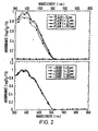
- the etch-stop property of a thin aluminium-lithium oxide layer is shown in Figure 2 .
- the poly( p -phenylene vinylene) is etched away significantly, in particular after prolonged exposure to the plasma.
- the traces in the bottom section of Figure 2 show an equivalent film of poly( p -phenylene vinylene) on a glass substrate but with an overlying layer of about 3.5nm of aluminium-lithium oxide deposited thereon by reactive DC magnetron sputtering from an aluminium-lithium target.
- the traces show very clearly that the thin oxide layer is very efficient in protecting the poly( p -phenylene vinylene) layer from the plasma etch, i.e., the oxide layer acts as an etch-stop.
- etch photolithography can be employed to form a patterned cathode 9.
- the barrier layer 7 is coated with a continuous layer of the material for the cathode 9.
- a photoresist is spun on top, patterned/exposed and developed.
- the layer is etched away (dry or wet-chemical etching) and finally, after etching is complete, the residual photoresist is removed.
- the continuous thin barrier layer which is a fluoride layer according to the invention acts as a protective layer and etch stop during the patterning process. It also acts as a buffer layer to reduce or eliminate possible edge effects at the edges of the pixels since these edges are not in direct contact with the organic layer. Without the barrier layer there would be a much greater risk of damaging the at least one organic layer and the interface with the top electrode where the top electrode is, for example, patterned to fabricate dot-matrix displays. Furthermore, the thin barrier layer also protects the organic layers to some degree against the ingress of, for example, oxygen and moisture, where no thick cathode layer is present.
Landscapes
- Physics & Mathematics (AREA)
- Optics & Photonics (AREA)
- Electroluminescent Light Sources (AREA)
- Materials For Medical Uses (AREA)
- Magnetic Heads (AREA)
- Oxygen, Ozone, And Oxides In General (AREA)
- Led Devices (AREA)
Claims (7)
- Organisches, lichtemittierendes Bauelement, umfassend:einen Träger (1); eine erste leitende Schicht (3), die auf dem Träger ausgebildet ist; mindestens eine auf der ersten leitenden Schicht ausgebildete Schicht eines lichtemittierenden organischen Materials (5); und eine zweite leitende Schicht (9), die über der mindestens einen Schicht des lichtemittierenden, organischen Materials ausgebildet ist,dadurch gekennzeichnet,
dass es zusätzlich eine einzelne elektrische Fluorid-Schicht (7) gibt, wobei sich diese einzelne dielektrische Fluorid-Schicht zwischen der mindestens einen Schicht eines lichtemittierenden, organischen Materials und der zweiten leitenden Schicht befindet und wobei die Fluorid-Schicht eine Dicke zwischen 1 und 10 nm aufweist. - Organisches, lichtemittierendes Bauelement nach Anspruch 1, wobei die Fluorid-Schicht eine Schicht des Ca-Fluorids oder Mg-Fluorids ist.
- Organisches, lichtemittierendes Bauelement nach Anspruch 1 oder 2, wobei der Flächenwiderstand der Fluorid-Schicht mindestens 1 MΩ/Quadrat beträgt.
- Organisches, lichtemittierendes Bauelement nach einem der vorangegangenen Ansprüche, wobei die zweite leitende Schicht strukturiert ist.
- Organisches, lichtemittierendes Bauelement nach einem der vorangegangenen Ansprüche, wobei die mindestens eine Schicht des organischen, lichtemittierenden Materials mindestens eines Schicht eines konjugierten Polymers umfasst.
- Organisches, lichtemittierendes Bauelement nach einem der vorangegangenen Ansprüche, wobei die zweite leitende Schicht die Kathode ist.
- Verfahren zur Herstellung eines organischen, lichtemittierenden Bauelements nach einem der vorangegangenen Ansprüche, wobei das Verfahren den Schritt des Aufbringens der zweiten leitenden Schicht (9) durch Kathodenzerstäubung umfasst.
Priority Applications (3)
| Application Number | Priority Date | Filing Date | Title |
|---|---|---|---|
| EP06075382A EP1672722A3 (de) | 1996-05-03 | 1997-05-02 | Organische lichtemittierende Vorrichtung und Verfahren zu ihrer Herstellung |
| EP06075364A EP1684368A3 (de) | 1996-05-03 | 1997-05-02 | Organische lichtemittierende Vorrichtung und Verfahren zu ihrer Herstellung |
| EP06075367A EP1672721A3 (de) | 1996-05-03 | 1997-05-02 | Organische lichtemittierende Vorrichtung und Verfahren zu ihrer Herstellung |
Applications Claiming Priority (3)
| Application Number | Priority Date | Filing Date | Title |
|---|---|---|---|
| GB9609282 | 1996-05-03 | ||
| GBGB9609282.0A GB9609282D0 (en) | 1996-05-03 | 1996-05-03 | Protective thin oxide layer |
| PCT/GB1997/001208 WO1997042666A1 (en) | 1996-05-03 | 1997-05-02 | Organic light-emitting device and method of fabricating the same |
Related Child Applications (3)
| Application Number | Title | Priority Date | Filing Date |
|---|---|---|---|
| EP06075367A Division EP1672721A3 (de) | 1996-05-03 | 1997-05-02 | Organische lichtemittierende Vorrichtung und Verfahren zu ihrer Herstellung |
| EP06075382A Division EP1672722A3 (de) | 1996-05-03 | 1997-05-02 | Organische lichtemittierende Vorrichtung und Verfahren zu ihrer Herstellung |
| EP06075364A Division EP1684368A3 (de) | 1996-05-03 | 1997-05-02 | Organische lichtemittierende Vorrichtung und Verfahren zu ihrer Herstellung |
Publications (3)
| Publication Number | Publication Date |
|---|---|
| EP0958622A1 EP0958622A1 (de) | 1999-11-24 |
| EP0958622B1 EP0958622B1 (de) | 2006-03-15 |
| EP0958622B2 true EP0958622B2 (de) | 2009-08-05 |
Family
ID=10793145
Family Applications (4)
| Application Number | Title | Priority Date | Filing Date |
|---|---|---|---|
| EP06075364A Withdrawn EP1684368A3 (de) | 1996-05-03 | 1997-05-02 | Organische lichtemittierende Vorrichtung und Verfahren zu ihrer Herstellung |
| EP06075382A Withdrawn EP1672722A3 (de) | 1996-05-03 | 1997-05-02 | Organische lichtemittierende Vorrichtung und Verfahren zu ihrer Herstellung |
| EP06075367A Withdrawn EP1672721A3 (de) | 1996-05-03 | 1997-05-02 | Organische lichtemittierende Vorrichtung und Verfahren zu ihrer Herstellung |
| EP97920818A Expired - Lifetime EP0958622B2 (de) | 1996-05-03 | 1997-05-02 | Organisches lichtemittierendes bauelement und dessen herstellung |
Family Applications Before (3)
| Application Number | Title | Priority Date | Filing Date |
|---|---|---|---|
| EP06075364A Withdrawn EP1684368A3 (de) | 1996-05-03 | 1997-05-02 | Organische lichtemittierende Vorrichtung und Verfahren zu ihrer Herstellung |
| EP06075382A Withdrawn EP1672722A3 (de) | 1996-05-03 | 1997-05-02 | Organische lichtemittierende Vorrichtung und Verfahren zu ihrer Herstellung |
| EP06075367A Withdrawn EP1672721A3 (de) | 1996-05-03 | 1997-05-02 | Organische lichtemittierende Vorrichtung und Verfahren zu ihrer Herstellung |
Country Status (6)
| Country | Link |
|---|---|
| US (4) | US6541790B1 (de) |
| EP (4) | EP1684368A3 (de) |
| AT (1) | ATE320663T1 (de) |
| DE (1) | DE69735483T3 (de) |
| GB (1) | GB9609282D0 (de) |
| WO (1) | WO1997042666A1 (de) |
Families Citing this family (48)
| Publication number | Priority date | Publication date | Assignee | Title |
|---|---|---|---|---|
| GB9609282D0 (en) | 1996-05-03 | 1996-07-10 | Cambridge Display Tech Ltd | Protective thin oxide layer |
| US5776622A (en) † | 1996-07-29 | 1998-07-07 | Eastman Kodak Company | Bilayer eletron-injeting electrode for use in an electroluminescent device |
| JP4142782B2 (ja) | 1998-06-26 | 2008-09-03 | Tdk株式会社 | 有機el素子 |
| JP3692844B2 (ja) * | 1998-07-24 | 2005-09-07 | セイコーエプソン株式会社 | 電界発光素子、及び電子機器 |
| JP2000173776A (ja) | 1998-12-07 | 2000-06-23 | Tdk Corp | 有機el素子 |
| JP2000252074A (ja) * | 1998-12-29 | 2000-09-14 | Tdk Corp | 有機el素子 |
| JP2000223272A (ja) | 1999-01-27 | 2000-08-11 | Tdk Corp | 有機el素子 |
| BR0011205A (pt) * | 1999-04-28 | 2002-02-19 | Du Pont | Dispositivo eletrônico orgânico flexível, display eletroluminescente, fotodetector e método de aperfeiçoamento da resistência à degradação do oxigênio e da umidade |
| KR100377321B1 (ko) * | 1999-12-31 | 2003-03-26 | 주식회사 엘지화학 | 피-형 반도체 성질을 갖는 유기 화합물을 포함하는 전기소자 |
| KR100721656B1 (ko) * | 2005-11-01 | 2007-05-23 | 주식회사 엘지화학 | 유기 전기 소자 |
| EP1173049B1 (de) * | 2000-02-02 | 2015-05-27 | Mitsubishi Chemical Corporation | Organisches elektrolumineszentes element |
| GB2361356B (en) * | 2000-04-14 | 2005-01-05 | Seiko Epson Corp | Light emitting device |
| US6670213B2 (en) | 2001-10-10 | 2003-12-30 | Cambridge Display Technology Limited | Method of preparing photoresponsive devices, and devices made thereby |
| GB0125620D0 (en) | 2001-10-25 | 2001-12-19 | Cambridge Display Tech Ltd | Monomers and low band gap polymers formed therefrom |
| GB0207134D0 (en) | 2002-03-27 | 2002-05-08 | Cambridge Display Tech Ltd | Method of preparation of organic optoelectronic and electronic devices and devices thereby obtained |
| US20050158454A1 (en) * | 2002-04-04 | 2005-07-21 | Dielectric Systems, Inc. | Method and system for forming an organic light-emitting device display having a plurality of passive polymer layers |
| JP2003317969A (ja) * | 2002-04-19 | 2003-11-07 | Print Labo Kk | El発光装置 |
| GB0215309D0 (en) | 2002-07-03 | 2002-08-14 | Cambridge Display Tech Ltd | Combined information display and information input device |
| GB0226010D0 (en) | 2002-11-08 | 2002-12-18 | Cambridge Display Tech Ltd | Polymers for use in organic electroluminescent devices |
| GB0229653D0 (en) | 2002-12-20 | 2003-01-22 | Cambridge Display Tech Ltd | Electrical connection of optoelectronic devices |
| JP4429917B2 (ja) * | 2002-12-26 | 2010-03-10 | 株式会社半導体エネルギー研究所 | 発光装置、表示装置及び電子機器 |
| US6790594B1 (en) * | 2003-03-20 | 2004-09-14 | Eastman Kodak Company | High absorption donor substrate coatable with organic layer(s) transferrable in response to incident laser light |
| GB0311234D0 (en) | 2003-05-16 | 2003-06-18 | Isis Innovation | Organic phosphorescent material and organic optoelectronic device |
| GB2404284B (en) * | 2003-07-10 | 2007-02-21 | Dainippon Printing Co Ltd | Organic electroluminescent element |
| US6953705B2 (en) * | 2003-07-22 | 2005-10-11 | E. I. Du Pont De Nemours And Company | Process for removing an organic layer during fabrication of an organic electronic device |
| KR100663624B1 (ko) * | 2004-04-29 | 2007-01-02 | 엘지.필립스 엘시디 주식회사 | 액정표시장치 제조방법 |
| EP1627891A1 (de) | 2004-08-11 | 2006-02-22 | Covion Organic Semiconductors GmbH | Polymere zur Verwendung in elektrolumineszierenden Anordnungen |
| KR20070097085A (ko) * | 2004-12-30 | 2007-10-02 | 이 아이 듀폰 디 네모아 앤드 캄파니 | 조사를 사용하는 장치 패턴화 |
| KR20060091648A (ko) * | 2005-02-16 | 2006-08-21 | 삼성에스디아이 주식회사 | 다층 캐소드를 포함하는 유기 발광 소자 |
| US7822616B2 (en) * | 2005-08-30 | 2010-10-26 | Lg Electronics Inc. | Time slot position coding of multiple frame types |
| CN101371619B (zh) | 2006-01-18 | 2013-11-13 | Lg化学株式会社 | 具有堆叠式有机发光单元的oled |
| US20070194321A1 (en) * | 2006-02-17 | 2007-08-23 | Semiconductor Energy Laboratory Co., Ltd. | Light emitting element, light emitting device, and electronic device |
| EP1821579A3 (de) * | 2006-02-17 | 2008-04-02 | Semiconductor Energy Laboratory Co., Ltd. | Lichtemittierendes Element, lichtemittierende Vorrichtung und elektronisches Gerät |
| CN101401487B (zh) * | 2006-03-07 | 2013-04-24 | Lg化学株式会社 | 有机发光器件及其制备方法 |
| US20080100202A1 (en) * | 2006-11-01 | 2008-05-01 | Cok Ronald S | Process for forming oled conductive protective layer |
| US7646144B2 (en) | 2006-12-27 | 2010-01-12 | Eastman Kodak Company | OLED with protective bi-layer electrode |
| US7750558B2 (en) | 2006-12-27 | 2010-07-06 | Global Oled Technology Llc | OLED with protective electrode |
| CA2678798C (en) * | 2007-03-19 | 2017-06-20 | Nanosys, Inc. | Methods for encapsulating nanocrystals |
| US20100155749A1 (en) * | 2007-03-19 | 2010-06-24 | Nanosys, Inc. | Light-emitting diode (led) devices comprising nanocrystals |
| US20100110728A1 (en) * | 2007-03-19 | 2010-05-06 | Nanosys, Inc. | Light-emitting diode (led) devices comprising nanocrystals |
| JP2010157493A (ja) * | 2008-12-02 | 2010-07-15 | Sony Corp | 表示装置およびその製造方法 |
| US11198270B2 (en) | 2008-12-30 | 2021-12-14 | Nanosys, Inc. | Quantum dot films, lighting devices, and lighting methods |
| US10214686B2 (en) | 2008-12-30 | 2019-02-26 | Nanosys, Inc. | Methods for encapsulating nanocrystals and resulting compositions |
| US8343575B2 (en) | 2008-12-30 | 2013-01-01 | Nanosys, Inc. | Methods for encapsulating nanocrystals and resulting compositions |
| JP5453952B2 (ja) * | 2009-06-23 | 2014-03-26 | ソニー株式会社 | 有機エレクトロルミネッセンス素子およびその製造方法、並びに表示装置およびその製造方法 |
| GB2475247B (en) * | 2009-11-10 | 2012-06-13 | Cambridge Display Tech Ltd | Organic optoelectronic device and method |
| EP2638321B1 (de) | 2010-11-10 | 2019-05-08 | Nanosys, Inc. | Quantenpunktfilme, beleuchtungsvorrichtungen und beleuchtungsverfahren |
| CN104124372A (zh) * | 2013-04-24 | 2014-10-29 | 海洋王照明科技股份有限公司 | 一种有机电致发光器件及其制备方法 |
Family Cites Families (34)
| Publication number | Priority date | Publication date | Assignee | Title |
|---|---|---|---|---|
| US4539507A (en) | 1983-03-25 | 1985-09-03 | Eastman Kodak Company | Organic electroluminescent devices having improved power conversion efficiencies |
| JPS60182692A (ja) | 1984-02-29 | 1985-09-18 | ホ−ヤ株式会社 | 薄膜el素子とその製造方法 |
| US4720532A (en) * | 1986-08-22 | 1988-01-19 | Massachusetts Institute Of Technology | Organopolysilazane precursors to silicon nitride-rich mixed SiC/Si3 N4 |
| US4720432A (en) | 1987-02-11 | 1988-01-19 | Eastman Kodak Company | Electroluminescent device with organic luminescent medium |
| JPH0266873A (ja) * | 1988-06-27 | 1990-03-06 | Eastman Kodak Co | 電界発光デバイス |
| US5085946A (en) | 1989-01-13 | 1992-02-04 | Ricoh Company, Ltd. | Electroluminescence device |
| EP0390551B1 (de) | 1989-03-31 | 1996-07-10 | Kabushiki Kaisha Toshiba | Organische elektrolumineszente Vorrichtung |
| GB8909011D0 (en) | 1989-04-20 | 1989-06-07 | Friend Richard H | Electroluminescent devices |
| EP0439627B1 (de) | 1989-08-18 | 1996-07-10 | Idemitsu Kosan Company Limited | Organisches elektrolumineszentes element |
| JP2895868B2 (ja) * | 1989-08-21 | 1999-05-24 | 出光興産株式会社 | 有機エレクトロルミネッセンス素子 |
| DE69110922T2 (de) | 1990-02-23 | 1995-12-07 | Sumitomo Chemical Co | Organisch elektrolumineszente Vorrichtung. |
| JP2776040B2 (ja) | 1990-04-27 | 1998-07-16 | 凸版印刷株式会社 | 有機薄膜el素子 |
| US5059861A (en) | 1990-07-26 | 1991-10-22 | Eastman Kodak Company | Organic electroluminescent device with stabilizing cathode capping layer |
| US5059862A (en) | 1990-07-26 | 1991-10-22 | Eastman Kodak Company | Electroluminescent device with improved cathode |
| US5047687A (en) | 1990-07-26 | 1991-09-10 | Eastman Kodak Company | Organic electroluminescent device with stabilized cathode |
| JP2793383B2 (ja) * | 1991-06-24 | 1998-09-03 | 出光興産株式会社 | 有機エレクトロルミネッセンス素子 |
| US5294870A (en) * | 1991-12-30 | 1994-03-15 | Eastman Kodak Company | Organic electroluminescent multicolor image display device |
| JPH0668977A (ja) * | 1992-08-13 | 1994-03-11 | Konica Corp | 多色電界発光表示装置 |
| JP3300069B2 (ja) * | 1992-11-19 | 2002-07-08 | パイオニア株式会社 | 有機エレクトロルミネッセンス素子 |
| US5489383A (en) * | 1993-06-16 | 1996-02-06 | Hitachi Zosen Corporation | Screw type dewatering machine |
| US5491377A (en) * | 1993-08-03 | 1996-02-13 | Janusauskas; Albert | Electroluminescent lamp and method |
| JPH07166160A (ja) | 1993-12-16 | 1995-06-27 | Toppan Printing Co Ltd | 有機薄膜el素子 |
| JPH07211458A (ja) | 1994-01-17 | 1995-08-11 | Fuji Electric Co Ltd | 薄膜発光素子 |
| JPH08102360A (ja) * | 1994-09-29 | 1996-04-16 | Toyota Central Res & Dev Lab Inc | 有機無機複合薄膜型電界発光素子 |
| JP3529543B2 (ja) | 1995-04-27 | 2004-05-24 | パイオニア株式会社 | 有機エレクトロルミネッセンス素子 |
| JPH08325564A (ja) | 1995-06-05 | 1996-12-10 | Nec Corp | 有機薄膜el素子 |
| DE19532064A1 (de) | 1995-08-31 | 1997-03-06 | Bosch Gmbh Robert | Elektrolumineszierendes Schichtsystem |
| GB9609282D0 (en) * | 1996-05-03 | 1996-07-10 | Cambridge Display Tech Ltd | Protective thin oxide layer |
| US5776622A (en) | 1996-07-29 | 1998-07-07 | Eastman Kodak Company | Bilayer eletron-injeting electrode for use in an electroluminescent device |
| US5714838A (en) * | 1996-09-20 | 1998-02-03 | International Business Machines Corporation | Optically transparent diffusion barrier and top electrode in organic light emitting diode structures |
| US6274979B1 (en) * | 1997-09-17 | 2001-08-14 | Texas Instruments Incorporated | Organic light emitting diodes |
| US6172459B1 (en) | 1998-07-28 | 2001-01-09 | Eastman Kodak Company | Electron-injecting layer providing a modified interface between an organic light-emitting structure and a cathode buffer layer |
| JP2000340366A (ja) * | 1999-05-27 | 2000-12-08 | Tdk Corp | 発光ダイオード |
| JP4212284B2 (ja) | 2002-03-12 | 2009-01-21 | パナソニック株式会社 | マグネトロン駆動用昇圧トランス |
-
1996
- 1996-05-03 GB GBGB9609282.0A patent/GB9609282D0/en active Pending
-
1997
- 1997-05-02 US US09/180,037 patent/US6541790B1/en not_active Expired - Lifetime
- 1997-05-02 WO PCT/GB1997/001208 patent/WO1997042666A1/en not_active Ceased
- 1997-05-02 EP EP06075364A patent/EP1684368A3/de not_active Withdrawn
- 1997-05-02 EP EP06075382A patent/EP1672722A3/de not_active Withdrawn
- 1997-05-02 EP EP06075367A patent/EP1672721A3/de not_active Withdrawn
- 1997-05-02 AT AT97920818T patent/ATE320663T1/de not_active IP Right Cessation
- 1997-05-02 DE DE69735483T patent/DE69735483T3/de not_active Expired - Lifetime
- 1997-05-02 EP EP97920818A patent/EP0958622B2/de not_active Expired - Lifetime
-
2003
- 2003-01-24 US US10/350,129 patent/US6881598B2/en not_active Expired - Lifetime
-
2005
- 2005-04-07 US US11/101,042 patent/US7394093B2/en not_active Expired - Fee Related
-
2008
- 2008-05-23 US US12/126,263 patent/US7786474B2/en not_active Expired - Fee Related
Also Published As
| Publication number | Publication date |
|---|---|
| WO1997042666A1 (en) | 1997-11-13 |
| EP1672721A3 (de) | 2010-06-30 |
| GB9609282D0 (en) | 1996-07-10 |
| EP1672722A3 (de) | 2010-06-30 |
| US20030151356A1 (en) | 2003-08-14 |
| US20080278071A1 (en) | 2008-11-13 |
| EP1672721A2 (de) | 2006-06-21 |
| DE69735483T2 (de) | 2006-11-23 |
| US6881598B2 (en) | 2005-04-19 |
| EP1684368A2 (de) | 2006-07-26 |
| EP0958622A1 (de) | 1999-11-24 |
| EP0958622B1 (de) | 2006-03-15 |
| DE69735483D1 (de) | 2006-05-11 |
| DE69735483T3 (de) | 2009-12-03 |
| ATE320663T1 (de) | 2006-04-15 |
| US20050181526A1 (en) | 2005-08-18 |
| US6541790B1 (en) | 2003-04-01 |
| EP1684368A3 (de) | 2010-06-30 |
| US7394093B2 (en) | 2008-07-01 |
| EP1672722A2 (de) | 2006-06-21 |
| US7786474B2 (en) | 2010-08-31 |
Similar Documents
| Publication | Publication Date | Title |
|---|---|---|
| EP0958622B2 (de) | Organisches lichtemittierendes bauelement und dessen herstellung | |
| US7190112B2 (en) | Photoresist mask/smoothing layer ensuring the field homogeneity and better step-coverage in OLED displays | |
| US5276380A (en) | Organic electroluminescent image display device | |
| US7160633B2 (en) | Structure-defining materials for OLEDs | |
| US6013538A (en) | Method of fabricating and patterning OLEDs | |
| US6297516B1 (en) | Method for deposition and patterning of organic thin film | |
| JP3948082B2 (ja) | 有機エレクトロルミネッセンス素子の製造方法 | |
| EP0951073B1 (de) | Polymere organische elektroluminezente Pixel-Vorrichtung und Verfahren zur Herstellung | |
| US6582888B1 (en) | Method for producing organic electroluminescent components | |
| WO1998059356A1 (en) | Passive matrix oled display and method of forming the same | |
| US20040212298A1 (en) | Structured electrodes | |
| HK1092946A (en) | Organic light-emittiing device and method of fabricating the same | |
| HK1092945A (en) | Organic light-emitting device and method of fabricating the same | |
| HK1092944A (en) | Organic light-emitting device and method of fabricating the same | |
| JP3900611B2 (ja) | 電界発光素子及びその製造方法 | |
| JP3728615B2 (ja) | 電界発光素子及びその製造方法 | |
| CA2397857C (en) | Oled devices with photoresist mask/smoothing layer | |
| KR100415433B1 (ko) | 유기 전계 발광 소자 및 그의 제조 방법 | |
| KR20030030792A (ko) | 유기 전계 발광 소자 및 그의 제조 방법 | |
| JPH0566423A (ja) | 液晶表示装置 | |
| JP2002373789A (ja) | 有機発光ダイオード及びその製造方法 |
Legal Events
| Date | Code | Title | Description |
|---|---|---|---|
| PUAI | Public reference made under article 153(3) epc to a published international application that has entered the european phase |
Free format text: ORIGINAL CODE: 0009012 |
|
| 17P | Request for examination filed |
Effective date: 19990312 |
|
| AK | Designated contracting states |
Kind code of ref document: A1 Designated state(s): AT BE CH DE DK ES FI FR GB GR IE IT LI LU MC NL PT SE |
|
| RIN1 | Information on inventor provided before grant (corrected) |
Inventor name: PICHLER, KARL |
|
| 17Q | First examination report despatched |
Effective date: 20020821 |
|
| 111Z | Information provided on other rights and legal means of execution |
Free format text: ATBECHDEDKESFIFRGBGRIEITLILUMCNLPTSE Effective date: 20040930 |
|
| GRAP | Despatch of communication of intention to grant a patent |
Free format text: ORIGINAL CODE: EPIDOSNIGR1 |
|
| GRAS | Grant fee paid |
Free format text: ORIGINAL CODE: EPIDOSNIGR3 |
|
| GRAA | (expected) grant |
Free format text: ORIGINAL CODE: 0009210 |
|
| AK | Designated contracting states |
Kind code of ref document: B1 Designated state(s): AT BE CH DE DK ES FI FR GB GR IE IT LI LU MC NL PT SE |
|
| PG25 | Lapsed in a contracting state [announced via postgrant information from national office to epo] |
Ref country code: LI Free format text: LAPSE BECAUSE OF FAILURE TO SUBMIT A TRANSLATION OF THE DESCRIPTION OR TO PAY THE FEE WITHIN THE PRESCRIBED TIME-LIMIT Effective date: 20060315 Ref country code: IT Free format text: LAPSE BECAUSE OF FAILURE TO SUBMIT A TRANSLATION OF THE DESCRIPTION OR TO PAY THE FEE WITHIN THE PRESCRIBED TIME-LIMIT;WARNING: LAPSES OF ITALIAN PATENTS WITH EFFECTIVE DATE BEFORE 2007 MAY HAVE OCCURRED AT ANY TIME BEFORE 2007. THE CORRECT EFFECTIVE DATE MAY BE DIFFERENT FROM THE ONE RECORDED. Effective date: 20060315 Ref country code: FI Free format text: LAPSE BECAUSE OF FAILURE TO SUBMIT A TRANSLATION OF THE DESCRIPTION OR TO PAY THE FEE WITHIN THE PRESCRIBED TIME-LIMIT Effective date: 20060315 Ref country code: CH Free format text: LAPSE BECAUSE OF FAILURE TO SUBMIT A TRANSLATION OF THE DESCRIPTION OR TO PAY THE FEE WITHIN THE PRESCRIBED TIME-LIMIT Effective date: 20060315 Ref country code: BE Free format text: LAPSE BECAUSE OF FAILURE TO SUBMIT A TRANSLATION OF THE DESCRIPTION OR TO PAY THE FEE WITHIN THE PRESCRIBED TIME-LIMIT Effective date: 20060315 Ref country code: AT Free format text: LAPSE BECAUSE OF FAILURE TO SUBMIT A TRANSLATION OF THE DESCRIPTION OR TO PAY THE FEE WITHIN THE PRESCRIBED TIME-LIMIT Effective date: 20060315 |
|
| REG | Reference to a national code |
Ref country code: GB Ref legal event code: FG4D Ref country code: CH Ref legal event code: EP |
|
| RIC1 | Information provided on ipc code assigned before grant |
Ipc: H01L 27/15 20060101ALI20060120BHEP Ipc: H01L 51/52 20060101AFI20060120BHEP |
|
| REG | Reference to a national code |
Ref country code: IE Ref legal event code: FG4D |
|
| PG25 | Lapsed in a contracting state [announced via postgrant information from national office to epo] |
Ref country code: IE Free format text: LAPSE BECAUSE OF NON-PAYMENT OF DUE FEES Effective date: 20060502 |
|
| REF | Corresponds to: |
Ref document number: 69735483 Country of ref document: DE Date of ref document: 20060511 Kind code of ref document: P |
|
| PGFP | Annual fee paid to national office [announced via postgrant information from national office to epo] |
Ref country code: FR Payment date: 20060517 Year of fee payment: 10 |
|
| PGFP | Annual fee paid to national office [announced via postgrant information from national office to epo] |
Ref country code: NL Payment date: 20060524 Year of fee payment: 10 |
|
| PG25 | Lapsed in a contracting state [announced via postgrant information from national office to epo] |
Ref country code: MC Free format text: LAPSE BECAUSE OF NON-PAYMENT OF DUE FEES Effective date: 20060531 |
|
| PG25 | Lapsed in a contracting state [announced via postgrant information from national office to epo] |
Ref country code: SE Free format text: LAPSE BECAUSE OF FAILURE TO SUBMIT A TRANSLATION OF THE DESCRIPTION OR TO PAY THE FEE WITHIN THE PRESCRIBED TIME-LIMIT Effective date: 20060615 Ref country code: DK Free format text: LAPSE BECAUSE OF FAILURE TO SUBMIT A TRANSLATION OF THE DESCRIPTION OR TO PAY THE FEE WITHIN THE PRESCRIBED TIME-LIMIT Effective date: 20060615 |
|
| PG25 | Lapsed in a contracting state [announced via postgrant information from national office to epo] |
Ref country code: ES Free format text: LAPSE BECAUSE OF FAILURE TO SUBMIT A TRANSLATION OF THE DESCRIPTION OR TO PAY THE FEE WITHIN THE PRESCRIBED TIME-LIMIT Effective date: 20060626 |
|
| PG25 | Lapsed in a contracting state [announced via postgrant information from national office to epo] |
Ref country code: PT Free format text: LAPSE BECAUSE OF FAILURE TO SUBMIT A TRANSLATION OF THE DESCRIPTION OR TO PAY THE FEE WITHIN THE PRESCRIBED TIME-LIMIT Effective date: 20060816 |
|
| REG | Reference to a national code |
Ref country code: CH Ref legal event code: PL |
|
| ET | Fr: translation filed | ||
| PLBI | Opposition filed |
Free format text: ORIGINAL CODE: 0009260 |
|
| PLAX | Notice of opposition and request to file observation + time limit sent |
Free format text: ORIGINAL CODE: EPIDOSNOBS2 |
|
| 26 | Opposition filed |
Opponent name: EASTMAN KODAK COMPANY |
|
| NLR1 | Nl: opposition has been filed with the epo |
Opponent name: EASTMAN KODAK COMPANY |
|
| PLAF | Information modified related to communication of a notice of opposition and request to file observations + time limit |
Free format text: ORIGINAL CODE: EPIDOSCOBS2 |
|
| PLBB | Reply of patent proprietor to notice(s) of opposition received |
Free format text: ORIGINAL CODE: EPIDOSNOBS3 |
|
| PG25 | Lapsed in a contracting state [announced via postgrant information from national office to epo] |
Ref country code: NL Free format text: LAPSE BECAUSE OF NON-PAYMENT OF DUE FEES Effective date: 20071201 |
|
| NLV4 | Nl: lapsed or anulled due to non-payment of the annual fee |
Effective date: 20071201 |
|
| REG | Reference to a national code |
Ref country code: FR Ref legal event code: ST Effective date: 20080131 |
|
| PG25 | Lapsed in a contracting state [announced via postgrant information from national office to epo] |
Ref country code: GR Free format text: LAPSE BECAUSE OF FAILURE TO SUBMIT A TRANSLATION OF THE DESCRIPTION OR TO PAY THE FEE WITHIN THE PRESCRIBED TIME-LIMIT Effective date: 20060616 |
|
| PG25 | Lapsed in a contracting state [announced via postgrant information from national office to epo] |
Ref country code: LU Free format text: LAPSE BECAUSE OF NON-PAYMENT OF DUE FEES Effective date: 20060502 Ref country code: FR Free format text: LAPSE BECAUSE OF NON-PAYMENT OF DUE FEES Effective date: 20070531 |
|
| PUAH | Patent maintained in amended form |
Free format text: ORIGINAL CODE: 0009272 |
|
| STAA | Information on the status of an ep patent application or granted ep patent |
Free format text: STATUS: PATENT MAINTAINED AS AMENDED |
|
| 27A | Patent maintained in amended form |
Effective date: 20090805 |
|
| AK | Designated contracting states |
Kind code of ref document: B2 Designated state(s): AT BE CH DE DK ES FI FR GB GR IE IT LI LU MC NL PT SE |
|
| REG | Reference to a national code |
Ref country code: ES Ref legal event code: FD2A Effective date: 20060503 |
|
| PGFP | Annual fee paid to national office [announced via postgrant information from national office to epo] |
Ref country code: DE Payment date: 20160527 Year of fee payment: 20 Ref country code: GB Payment date: 20160527 Year of fee payment: 20 |
|
| REG | Reference to a national code |
Ref country code: DE Ref legal event code: R071 Ref document number: 69735483 Country of ref document: DE |
|
| REG | Reference to a national code |
Ref country code: GB Ref legal event code: PE20 Expiry date: 20170501 |
|
| PG25 | Lapsed in a contracting state [announced via postgrant information from national office to epo] |
Ref country code: GB Free format text: LAPSE BECAUSE OF EXPIRATION OF PROTECTION Effective date: 20170501 |