EP0944924B1 - Verfahren zum herstellen eines licht aussendenden und/oder empfangenden halbleiterkörpers - Google Patents
Verfahren zum herstellen eines licht aussendenden und/oder empfangenden halbleiterkörpers Download PDFInfo
- Publication number
- EP0944924B1 EP0944924B1 EP97918885A EP97918885A EP0944924B1 EP 0944924 B1 EP0944924 B1 EP 0944924B1 EP 97918885 A EP97918885 A EP 97918885A EP 97918885 A EP97918885 A EP 97918885A EP 0944924 B1 EP0944924 B1 EP 0944924B1
- Authority
- EP
- European Patent Office
- Prior art keywords
- layer
- semiconductor
- semiconductor body
- gap
- light
- Prior art date
- Legal status (The legal status is an assumption and is not a legal conclusion. Google has not performed a legal analysis and makes no representation as to the accuracy of the status listed.)
- Expired - Lifetime
Links
Images


Classifications
-
- H—ELECTRICITY
- H10—SEMICONDUCTOR DEVICES; ELECTRIC SOLID-STATE DEVICES NOT OTHERWISE PROVIDED FOR
- H10H—INORGANIC LIGHT-EMITTING SEMICONDUCTOR DEVICES HAVING POTENTIAL BARRIERS
- H10H20/00—Individual inorganic light-emitting semiconductor devices having potential barriers, e.g. light-emitting diodes [LED]
- H10H20/80—Constructional details
- H10H20/81—Bodies
- H10H20/8215—Bodies characterised by crystalline imperfections, e.g. dislocations; characterised by the distribution of dopants, e.g. delta-doping
-
- H—ELECTRICITY
- H10—SEMICONDUCTOR DEVICES; ELECTRIC SOLID-STATE DEVICES NOT OTHERWISE PROVIDED FOR
- H10F—INORGANIC SEMICONDUCTOR DEVICES SENSITIVE TO INFRARED RADIATION, LIGHT, ELECTROMAGNETIC RADIATION OF SHORTER WAVELENGTH OR CORPUSCULAR RADIATION
- H10F77/00—Constructional details of devices covered by this subclass
- H10F77/70—Surface textures, e.g. pyramid structures
-
- H—ELECTRICITY
- H10—SEMICONDUCTOR DEVICES; ELECTRIC SOLID-STATE DEVICES NOT OTHERWISE PROVIDED FOR
- H10F—INORGANIC SEMICONDUCTOR DEVICES SENSITIVE TO INFRARED RADIATION, LIGHT, ELECTROMAGNETIC RADIATION OF SHORTER WAVELENGTH OR CORPUSCULAR RADIATION
- H10F77/00—Constructional details of devices covered by this subclass
- H10F77/70—Surface textures, e.g. pyramid structures
- H10F77/703—Surface textures, e.g. pyramid structures of the semiconductor bodies, e.g. textured active layers
-
- H—ELECTRICITY
- H10—SEMICONDUCTOR DEVICES; ELECTRIC SOLID-STATE DEVICES NOT OTHERWISE PROVIDED FOR
- H10W—GENERIC PACKAGES, INTERCONNECTIONS, CONNECTORS OR OTHER CONSTRUCTIONAL DETAILS OF DEVICES COVERED BY CLASS H10
- H10W72/00—Interconnections or connectors in packages
- H10W72/851—Dispositions of multiple connectors or interconnections
- H10W72/874—On different surfaces
- H10W72/884—Die-attach connectors and bond wires
-
- H—ELECTRICITY
- H10—SEMICONDUCTOR DEVICES; ELECTRIC SOLID-STATE DEVICES NOT OTHERWISE PROVIDED FOR
- H10W—GENERIC PACKAGES, INTERCONNECTIONS, CONNECTORS OR OTHER CONSTRUCTIONAL DETAILS OF DEVICES COVERED BY CLASS H10
- H10W90/00—Package configurations
- H10W90/701—Package configurations characterised by the relative positions of pads or connectors relative to package parts
- H10W90/731—Package configurations characterised by the relative positions of pads or connectors relative to package parts of die-attach connectors
- H10W90/736—Package configurations characterised by the relative positions of pads or connectors relative to package parts of die-attach connectors between a chip and a stacked lead frame, conducting package substrate or heat sink
-
- H—ELECTRICITY
- H10—SEMICONDUCTOR DEVICES; ELECTRIC SOLID-STATE DEVICES NOT OTHERWISE PROVIDED FOR
- H10W—GENERIC PACKAGES, INTERCONNECTIONS, CONNECTORS OR OTHER CONSTRUCTIONAL DETAILS OF DEVICES COVERED BY CLASS H10
- H10W90/00—Package configurations
- H10W90/701—Package configurations characterised by the relative positions of pads or connectors relative to package parts
- H10W90/751—Package configurations characterised by the relative positions of pads or connectors relative to package parts of bond wires
- H10W90/756—Package configurations characterised by the relative positions of pads or connectors relative to package parts of bond wires between a chip and a stacked lead frame, conducting package substrate or heat sink
-
- Y—GENERAL TAGGING OF NEW TECHNOLOGICAL DEVELOPMENTS; GENERAL TAGGING OF CROSS-SECTIONAL TECHNOLOGIES SPANNING OVER SEVERAL SECTIONS OF THE IPC; TECHNICAL SUBJECTS COVERED BY FORMER USPC CROSS-REFERENCE ART COLLECTIONS [XRACs] AND DIGESTS
- Y02—TECHNOLOGIES OR APPLICATIONS FOR MITIGATION OR ADAPTATION AGAINST CLIMATE CHANGE
- Y02E—REDUCTION OF GREENHOUSE GAS [GHG] EMISSIONS, RELATED TO ENERGY GENERATION, TRANSMISSION OR DISTRIBUTION
- Y02E10/00—Energy generation through renewable energy sources
- Y02E10/50—Photovoltaic [PV] energy
Definitions
- the invention relates to a method for producing a light-emitting and / or receiving semiconductor body with at least one semiconductor layer which consists of GaAs x P 1-x with 0 ⁇ x ⁇ 1.
- EP 584 599 describes a light-emitting diode chip in which on a n-type GaP substrate an n-type GaP epitaxial layer and applied a p-type GaP epitaxial layer thereon is.
- the bottom of the GaP substrate is with a Contact metallization made of an Au-Ge alloy and on the top of the p-type GaP epitaxial layer applied a contact metallization, starting out from the p-type GaP epitaxial layer, for example an Au layer, an Au-Zn layer, a Ti-W-N layer and an Au or Al layer.
- light-emitting diodes are known in which on a GaP substrate a layer sequence of GaAsP is applied by means of epitaxy is.
- This layer sequence points out, for example a GaAsP transition layer from the GaP substrate with increasing As content, an n-doped GaAsP layer (Dopant: e.g. tellurium or sulfur) and a p-doped GaAsP layer (dopant: zinc).
- a contact metallization for example, starting from the p-doped GaAsP layer a gold-zinc layer, a TiWN layer and one There is an aluminum layer.
- the bottom of the GaP substrate is provided with a contact metallization, for example from a gold germanium layer applied to the GaP substrate consists.
- a semiconductor body described above can be used A light emitting diode can be made to emit light the range from yellow to super red.
- the disadvantage of this Semiconductor body is that in the semiconductor body only a fraction of the light generated from the semiconductor body is decoupled.
- a solar cell is described in US Pat. No. 4,582,952, which, based on a transparent GaP substrate, from a first p-doped GaAsP layer with graded As content, from a second p-doped GaAsP layer, from an n-doped GaAsP layer and from one GaP cover layer is built up.
- the GaP substrate and the GaP cover layers are each with a plurality of metal contacts Mistake.
- the object of the invention is to develop a method for producing a light-emitting and / or receiving semiconductor body with at least one semiconductor layer made of GaAs x P 1-x with 0 x x ⁇ 1, which has an improved coupling in and out of light.
- At least part of the surface of the semiconductor layer is treated in a first etching step with an etching solution of the composition H 2 SO 4 : H 2 O 2 : H 2 O and subsequently in a second etching step with dilute hydrofluoric acid, so that at least part of the surface of the semiconductor layer is roughened.
- the surface is advantageously roughened achieved that compared to a flat surface greater proportion of the radiation generated in the semiconductor body at an angle to the surface of the semiconductor layer that is smaller than the critical angle of total reflection is.
- Another advantage of the roughened semiconductor surface is that in a semiconductor device in which a semiconductor body directly from a plastic coating is surrounded, an increased adhesive strength between the Semiconductor body and the plastic coating is achieved. This creates the danger of the plastic covering becoming detached from the semiconductor body during operation and consequently accelerated aging of the semiconductor device is reduced.
- the method is used for a semiconductor body with an n-doped GaP substrate on which a layer sequence of GaAsP is applied, the entire free surface of the semiconductor body roughened.
- the free surface Part of the surface to understand that not with a Contact metallization layer is provided.
- the GaP substrate for the in the GaAsP layer sequence generated electromagnetic radiation permeable because the band gap of GaAsP is smaller than that by GaP. Therefore, the radiation can advantageously pass through the entire free surface of the semiconductor body be coupled out of this.
- One advantageously has an underside of the GaP substrate applied contact metallization at the border a mirror surface to the semiconductor body. This has to Consequence that of the GaAsP layer sequence in the direction of Contact metallization radiation emitted by this largely is reflected and subsequently by the free surface can be coupled out.
- the procedure and its training will be the second Etching step uses a 40-50% hydrofluoric acid.
- the second Etching step is carried out at a temperature between 15 and 30 °, performed especially at approx. 25 ° and lasts between 30 Minutes and 120 minutes.
- the semiconductor body has a GaP substrate on which a layer sequence of nitrogen (N) -doped GaP (short: GaP: N) is applied.
- N nitrogen
- the substrate for that in the GaP layer sequence generated radiation permeable, so that here too by the Roughening the semiconductor surface a significant increase the light decoupling is achieved.
- a layer sequence of GaAs x P 1-x with 0 x x ⁇ 1 or GaP: N is first applied to a substrate wafer made of GaP.
- a first contact metallization is then applied to the underside of the substrate wafer and a plurality of second contact metallizations are applied to the top of the layer sequence.
- the free surface of the layer sequence is first treated in a first etching step with the etching solution of the composition H 2 SO 4 : H 2 O 2 : H 2 O and in a second etching step with hydrofluoric acid (HF).
- the semiconductor wafer consisting of Substrate wafer, layer sequence, first and second contact metallizations to individual semiconductor bodies, e.g. B. LED chips, isolated.
- the side faces of the semiconductor body be roughened, the semiconductor wafer after the Application of the first and second contact metallizations for Example on an adhesive film or another holding device applied and in individual light emitting diode semiconductor body sporadically. Then the two above Etching steps are carried out before the isolated semiconductor body lifted off the holding means and z. B. too LEDs are processed further.
- the semiconductor body shown in FIG. 1 is a light-emitting semiconductor body, e.g. B. a light emitting diode semiconductor body.
- a light-emitting layer sequence 18 is arranged on a GaP substrate 1.
- a first GaAs x P 1-x epitaxial layer 2 with 0 x x ⁇ 1 is applied, over which in turn a second nAs-doped GaAs x P 1-x epitaxial layer 3 with 0 x x ⁇ 1 is arranged.
- Te or S can be used as the n-dopant.
- the underside of the GaP substrate 1 is provided with a first contact metallization 5, which consists, for example, of an Au-Ge alloy / Ag / Au layer sequence.
- a second contact metallization 6 is applied to the top of the third GaAs x P 1-x epitaxial layer 4.
- Any other combination of materials and layers known to the person skilled in the art to be suitable can also be used for the contact metallizations 5 and 6.
- the method for producing the roughening 8 consists of a first and a second etching step, the free surface 7 of the semiconductor body during the first etching step using an etching solution of the composition H 2 SO 4 : H 2 O 2 : H 2 O (3: 1: 1) and is treated with hydrofluoric acid (40 to 50%) in the second etching step.
- the first etching step is carried out at a temperature of between 15 and 80 °, especially 25 ° C and lasts between 30 seconds and 10 minutes.
- the second etching step is carried out at a temperature between 15 and 30 ° C and takes between 30 minutes and 120 minutes.
- the semiconductor body shown in Figure 2 also a Semiconductor body emitting light, in turn, has a GaP substrate 1 on. There is an n-doped first on the GaP substrate GaP: N epitaxial layer 9 applied, over which a p-doped second GaP: N epitaxial layer 10 is arranged.
- N-doping of GaP becomes a narrowing of the band gap reached, causing the GaP substrate to turn for that in layer sequence 17 from first 9 and second 10 GaP: N epitaxial layer generated light is transparent.
- FIG. 1 Another difference from the semiconductor body shown in FIG. 1 is that only the top 11 of the Semiconductor body is provided with a roughening 8 and the Side surfaces 12 are not roughened. That to make the roughening 8 used method corresponds for example the method explained in connection with Figure 1.
- FIG. 2 shows an example of how the Semiconductor body in a conventional LED housing a first 19 and a second 20 electrical connection, an opaque body 21 and one translucent envelope 22, may be installed.
- the semiconductor body is, for example, electrical conductive solder or adhesive with its first Contact metallization 5 on the second electrical connection 20 attached.
- the second contact metallization 6 is by means of a bonding wire 23 with the first electrical connection 19 connected.
- the base body 21 partially encloses the electrical Connections 19, 20 and has a recess in the semiconductor body is arranged.
- the recess is for example shaped so that it is for that of the semiconductor body decoupled light forms a reflector.
- HOT STUFF is the recess with the translucent envelope 22 filled directly to the free surface 7 of the semiconductor body borders.
- the envelope 22 is, for example made of a transparent synthetic resin and forms with the roughening 8 of the semiconductor body has a micro toothing from the adhesive strength of the cladding 22 on the semiconductor body increases and thus the risk of delamination
- the semiconductor body of Figure 1 in such a Housing can be installed.
- the micro toothing forms then of course not only on the top of the semiconductor body but also on the side surfaces.
- the housing can also be made in one piece from a transparent Be made of plastic and have any shape.
- the semiconductor body of FIG. 1 can of course also be used be manufactured in such a way that it is only on its top 11 has a roughening 8.
- the semiconductor body can likewise of Figure 2 over its entire free surface 7 with a Roughening 8 are provided.
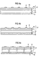
- the semiconductor wafer consisting of the GaP substrate, the first 2, second 3 and third 4 GaAs x P 1-x epitaxial layer, the first 5 and the second 6 contact metallizations, is placed on a holding means 16, for example one Adhesive film, applied and separated into individual semiconductor bodies. This is done, for example, using saws.
- the finished, roughened semiconductor body can then be separated from the holding means 16 and for example processed into LEDs.
- the process sequence shown schematically in FIG simultaneous production of a plurality of semiconductor bodies 2 differs from that of FIG essentially in that the first and the second etching step is carried out before the semiconductor wafer is separated. This ensures that only a part, namely not part of the upper side covered by the contact metallizations 6 11 of the semiconductor wafer with a roughening 8 becomes.
Landscapes
- Led Devices (AREA)
- Weting (AREA)
- Semiconductor Lasers (AREA)
Abstract
Description
Claims (9)
- Verfahren zum Herstellen eines Licht aussendenden und/oder empfangenden Halbleiterkörpers mit mindestens einer Halbleiterschicht, die aus GaAsxP1-x mit 0 ≤ X < 1 besteht, dadurch gekennzeichnet, daß zumindest ein Teil der Oberfläche der Halbleiterschicht in einem ersten Ätzschritt mit einer Ätzlösung der Zusammensetzung H2SO4:H2O2:H2O und nachfolgend in einem zweiten Ätzschritt mit Flußsäure behandelt wird, so daß zumindest auf dem Teil der Oberfläche der Halbleiterschicht eine Aufrauhung (8) erzeugt wird.
- Verfahren nach Anspruch 1, dadurch gekennzeichnet, daß die Aufrauhung (8) die Gestalt von nebeneinander angeordneten Sägezähnen aufweist.
- Verfahren nach Anspruch 1 oder 2, dadurch gekennzeichnet, daß ein Halbleiterkörper mit einem GaP-Substrat verwendet wird, auf dem eine Schichtenfolge (17,18) aufgebracht ist, die mindestens eine mit Stickstoff dotierte GaP-Epitaxieschicht aufweist.
- Verfahren nach Anspruch 1 oder 2, dadurch gekennzeichnet, daß ein Halbleiterkörper mit einem GaP-Substrat verwendet wird, auf dem eine Schichtenfolge (17,18) aufgebracht ist, die mindestens eine GaAsxP1-x-Epitaxieschicht mit 0 < x < 1 aufweist.
- Verfahren nach einem der Ansprüche 1 bis 4, dadurch gekennzeichnet, daß die gesamte freie Oberfläche (7) des Halbleiterkörpers die Aufrauhung (8) aufweist.
- Verfahren zum gleichzeitigen Herstellen einer Mehrzahl von Licht aussendenden und/oder empfangenden Halbleiterkörpern mit mindestens einer Halbleiterschicht, die aus GaAsxP1-x mit 0 ≤ x < 1 bzw. aus GaP:N besteht, das die folgenden Schritte enthält:a) zunächst wird auf eine Substratscheibe (13) aus GaP eine Schichtenfolge (17,18) aus GaAsxP1-x mit 0 ≤ x < 1 aufgebracht,b) auf die Unterseite (14) der Substratscheibe (13) wird eine erste Kontaktmetallisierung (5) und auf die Oberseite (15) der Schichtenfolge (17,18) mindestens eine zweite Kontaktmetallisierung (6) aufgebracht ,c) die freie Oberfläche der Schichtenfolge (17, 18) wird zunächst in einem ersten Ätzschritt mit einer Ätzlösung der Zusammensetzung H2SO4:H2O2:H2O und in einem zweiten Ätzschritt mit Flußsäure (HF) behandelt , so daß eine Aufrauhung (8) der freien Oberfläche erzeugt wird undd) die Halbleiterscheibe, bestehend aus der Substratscheibe (13), der Schichtenfolge (17, 18), der ersten (5) und den zweiten (6) Kontaktmetallisierungen wird zu einzelnen Halbleiterkörpern vereinzelt.
- Verfahren zum gleichzeitigen Herstellen einer Mehrzahl von Licht aussendenden und/oder empfangenden Halbleiterkörpern mit mindestens einer Halbleiterschicht, die aus GaAsxP1-x mit 0 ≤ x < 1 bzw. aus GaP:N besteht, das die folgenden Schritte enthält:a) zunächst wird auf eine Substratscheibe (13) aus GaP eine Schichtenfolge (17,18) aus GaAsxP1-x mit 0 ≤ x < 1 aufgebracht,b) auf die Unterseite (14) der Substratscheibe (13) wird eine erste Kontaktmetallisierung (5) und auf die Oberseite (15) der Schichtenfolge (17,18) eine Mehrzahl von zweiten Kontaktmetallisierungen (6) aufgebracht,c) die Halbleiterscheibe, bestehend aus der Substratscheibe (13), der Schichtenfolge (17,18), der ersten (5) und den zweiten (6) Kontaktmetallisierungen, wird auf einem Haltemittel (16) aufgebracht ,d) die Halbleiterscheibe wird zu einzelnen Halbleiterkörpern vereinzelt unde) die freien Oberflächen der Halbleiterkörper werden zunächst in einem ersten Ätzschritt mit einer Ätzlösung der Zusammensetzung H2SO4:H2O2:H2O und in einem zweiten Ätzschritt mit Flußsäure (HF) behandelt , so daß eine Aufrauhung (8) der Oberflächen erzeugt wird.
- Verfahren nach einem der Ansprüche 1 bis 7, dadurch gekennzeichnet, daß beim ersten Ätzschritt für die Ätzlösung H2SO4:H2O2:H2O ein Verhältnis von 3:1:1, eine Temperatur zwischen 15 und 80°C und eine Ätzdauer zwischen einer halben Minute und 10 Minuten gewählt wird.
- Verfahren nach einem der Ansprüche 1 bis 8, dadurch gekennzeichnet, daß beim zweiten Ätzschritt eine 40-50%ige Flußsäure, eine Temperatur zwischen 15 und 30°C und eine Ätzdauer zwischen 30 Minuten und 120 Minuten gewählt wird.
Applications Claiming Priority (3)
| Application Number | Priority Date | Filing Date | Title |
|---|---|---|---|
| DE19632627A DE19632627A1 (de) | 1996-08-13 | 1996-08-13 | Verfahren zum Herstellen eines Licht aussendenden und/oder empfangenden Halbleiterkörpers |
| DE19632627 | 1996-08-13 | ||
| PCT/DE1997/001729 WO1998007195A1 (de) | 1996-08-13 | 1997-08-13 | Verfahren zum herstellen eines licht aussendenden und/oder empfangenden halbleiterkörpers |
Publications (2)
| Publication Number | Publication Date |
|---|---|
| EP0944924A1 EP0944924A1 (de) | 1999-09-29 |
| EP0944924B1 true EP0944924B1 (de) | 2002-10-23 |
Family
ID=7802534
Family Applications (1)
| Application Number | Title | Priority Date | Filing Date |
|---|---|---|---|
| EP97918885A Expired - Lifetime EP0944924B1 (de) | 1996-08-13 | 1997-08-13 | Verfahren zum herstellen eines licht aussendenden und/oder empfangenden halbleiterkörpers |
Country Status (7)
| Country | Link |
|---|---|
| US (1) | US6531405B1 (de) |
| EP (1) | EP0944924B1 (de) |
| JP (1) | JP2001501365A (de) |
| CN (1) | CN1227748C (de) |
| DE (2) | DE19632627A1 (de) |
| TW (1) | TW353237B (de) |
| WO (1) | WO1998007195A1 (de) |
Families Citing this family (36)
| Publication number | Priority date | Publication date | Assignee | Title |
|---|---|---|---|---|
| DE10006738C2 (de) | 2000-02-15 | 2002-01-17 | Osram Opto Semiconductors Gmbh | Lichtemittierendes Bauelement mit verbesserter Lichtauskopplung und Verfahren zu seiner Herstellung |
| US7205578B2 (en) | 2000-02-15 | 2007-04-17 | Osram Gmbh | Semiconductor component which emits radiation, and method for producing the same |
| US6791119B2 (en) * | 2001-02-01 | 2004-09-14 | Cree, Inc. | Light emitting diodes including modifications for light extraction |
| US6909162B2 (en) * | 2001-11-02 | 2005-06-21 | Omnivision Technologies, Inc. | Surface passivation to reduce dark current in a CMOS image sensor |
| US6462365B1 (en) * | 2001-11-06 | 2002-10-08 | Omnivision Technologies, Inc. | Active pixel having reduced dark current in a CMOS image sensor |
| TW576864B (en) * | 2001-12-28 | 2004-02-21 | Toshiba Corp | Method for manufacturing a light-emitting device |
| JP3715627B2 (ja) * | 2002-01-29 | 2005-11-09 | 株式会社東芝 | 半導体発光素子及びその製造方法 |
| DE10203809B4 (de) * | 2002-01-31 | 2010-05-27 | Osram Opto Semiconductors Gmbh | Strahlungsemittierendes Halbleiterbauelement |
| JP3705791B2 (ja) * | 2002-03-14 | 2005-10-12 | 株式会社東芝 | 半導体発光素子および半導体発光装置 |
| JP3776824B2 (ja) * | 2002-04-05 | 2006-05-17 | 株式会社東芝 | 半導体発光素子およびその製造方法 |
| DE10229231B9 (de) * | 2002-06-28 | 2006-05-11 | Osram Opto Semiconductors Gmbh | Verfahren zum Herstellen eines Strahlung emittierenden und/oder empfangenden Halbleiterchips mit einer Strahlungsein- und/oder -auskoppel-Mikrostruktur |
| DE10324909B4 (de) * | 2003-05-30 | 2017-09-07 | Osram Opto Semiconductors Gmbh | Gehäuse für ein strahlungsemittierendes Bauelement, Verfahren zu dessen Herstellung und strahlungsemittierendes Bauelement |
| JP4315744B2 (ja) * | 2003-06-25 | 2009-08-19 | 株式会社沖データ | 積層体及び半導体装置の製造方法 |
| TW200505042A (en) * | 2003-07-17 | 2005-02-01 | South Epitaxy Corp | LED device |
| WO2005088733A1 (ja) * | 2004-03-12 | 2005-09-22 | Kyosemi Corporation | 積層型太陽電池 |
| US7772605B2 (en) * | 2004-03-19 | 2010-08-10 | Showa Denko K.K. | Compound semiconductor light-emitting device |
| JP4092658B2 (ja) * | 2004-04-27 | 2008-05-28 | 信越半導体株式会社 | 発光素子の製造方法 |
| CN100481534C (zh) * | 2004-10-28 | 2009-04-22 | 晶元光电股份有限公司 | 发光二极管及其制造方法 |
| JP4692072B2 (ja) * | 2005-05-19 | 2011-06-01 | 三菱化学株式会社 | 発光ダイオードの製造方法 |
| KR101154744B1 (ko) * | 2005-08-01 | 2012-06-08 | 엘지이노텍 주식회사 | 질화물 발광 소자 및 그 제조 방법 |
| TWI396307B (zh) * | 2009-02-05 | 2013-05-11 | Huga Optotech Inc | 發光二極體 |
| TWI470823B (zh) | 2009-02-11 | 2015-01-21 | Epistar Corp | 發光元件及其製造方法 |
| TWI408832B (zh) * | 2009-03-30 | 2013-09-11 | Huga Optotech Inc | 具有中空結構之柱狀結構之發光元件及其形成方法 |
| JP2011035017A (ja) * | 2009-07-30 | 2011-02-17 | Hitachi Cable Ltd | 発光素子 |
| JP2011171327A (ja) * | 2010-02-16 | 2011-09-01 | Toshiba Corp | 発光素子およびその製造方法、並びに発光装置 |
| JP2012142444A (ja) * | 2010-12-28 | 2012-07-26 | Sharp Corp | 発光デバイス、透明導電膜の形成方法、発光デバイスの製造方法および電気機器 |
| US20130234149A1 (en) * | 2012-03-09 | 2013-09-12 | Electro Scientific Industries, Inc. | Sidewall texturing of light emitting diode structures |
| JP2015028984A (ja) * | 2013-07-30 | 2015-02-12 | 日亜化学工業株式会社 | 半導体発光素子 |
| JP6255192B2 (ja) * | 2013-09-04 | 2017-12-27 | 株式会社ディスコ | 光デバイス及び光デバイスの加工方法 |
| DE102013111503B4 (de) * | 2013-10-18 | 2021-08-05 | OSRAM Opto Semiconductors Gesellschaft mit beschränkter Haftung | Optoelektronischer Halbleiterchip, optoelektronisches Bauelement und Verfahren zur Vereinzelung von Halbleiterchips |
| CN105047777A (zh) * | 2015-08-26 | 2015-11-11 | 映瑞光电科技(上海)有限公司 | 具有粗化侧壁的led垂直芯片结构及制备方法 |
| CN105428475B (zh) * | 2015-12-17 | 2018-05-01 | 映瑞光电科技(上海)有限公司 | 垂直led芯片结构及其制备方法 |
| CN107482096B (zh) | 2017-08-11 | 2019-04-09 | 厦门市三安光电科技有限公司 | 一种发光装置及其制造方法 |
| WO2021164854A1 (en) * | 2020-02-18 | 2021-08-26 | Osram Opto Semiconductors Gmbh | Optoelectronic semiconductor device and method for producing an optoelectronic semiconductor device |
| US20210296176A1 (en) * | 2020-03-23 | 2021-09-23 | Semiconductor Components Industries, Llc | Structure and method for electronic die singulation using alignment structures and multi-step singulation |
| WO2022266918A1 (zh) * | 2021-06-24 | 2022-12-29 | 天津三安光电有限公司 | 一种发光二极管及制作方法 |
Family Cites Families (16)
| Publication number | Priority date | Publication date | Assignee | Title |
|---|---|---|---|---|
| JPS5856963B2 (ja) * | 1977-05-06 | 1983-12-17 | 三菱化成ポリテック株式会社 | 電子発光化合物半導体の製造方法 |
| DE3172935D1 (en) * | 1980-02-28 | 1986-01-02 | Toshiba Kk | Iii - v group compound semiconductor light-emitting element and method of producing the same |
| US4575577A (en) * | 1983-05-27 | 1986-03-11 | Chevron Research Company | Ternary III-V multicolor solar cells containing a quaternary window layer and a quaternary transition layer |
| DE3484266D1 (de) * | 1983-11-30 | 1991-04-18 | Sharp Kk | Halbleiterlaser-vorrichtung und verfahren zu deren herstellung. |
| US4582952A (en) * | 1984-04-30 | 1986-04-15 | Astrosystems, Inc. | Gallium arsenide phosphide top solar cell |
| EP0198199B1 (de) * | 1985-04-19 | 1992-06-17 | Siemens Aktiengesellschaft | Verfahren zur nasschemischen Herstellung eines Oberflächengitters mit einer bestimmten Gitterkonstante auf der Oberfläche eines Substrats aus einem Kristallmaterial |
| DE3610333A1 (de) * | 1985-04-19 | 1986-11-27 | Siemens AG, 1000 Berlin und 8000 München | Verfahren zur herstellung eines oberflaechengitters mit einer bestimmten gitterkonstanten auf einem tieferliegenden oberflaechenbereich einer mesastruktur |
| EP0218422B1 (de) * | 1985-09-30 | 1992-09-16 | Kabushiki Kaisha Toshiba | Lichtemittierendes Halbleiterelement |
| JP2953468B2 (ja) * | 1989-06-21 | 1999-09-27 | 三菱化学株式会社 | 化合物半導体装置及びその表面処理加工方法 |
| DE59308636D1 (de) * | 1992-08-28 | 1998-07-09 | Siemens Ag | Leuchtdiode |
| DE4305296C3 (de) * | 1993-02-20 | 1999-07-15 | Vishay Semiconductor Gmbh | Verfahren zum Herstellen einer strahlungsemittierenden Diode |
| US5436201A (en) * | 1993-05-28 | 1995-07-25 | Hughes Aircraft Company | Dual etchant process, particularly for gate recess fabrication in GaAs MMIC chips |
| US5689123A (en) * | 1994-04-07 | 1997-11-18 | Sdl, Inc. | III-V aresenide-nitride semiconductor materials and devices |
| JP2991616B2 (ja) * | 1994-06-30 | 1999-12-20 | シャープ株式会社 | 半導体発光素子 |
| JP2950362B2 (ja) * | 1995-03-15 | 1999-09-20 | 信越半導体株式会社 | 化合物半導体中の窒素濃度の測定方法 |
| US5869849A (en) * | 1995-10-05 | 1999-02-09 | Industry Technology Research Institute | Light-emitting diodes with high illumination |
-
1996
- 1996-08-13 DE DE19632627A patent/DE19632627A1/de not_active Withdrawn
-
1997
- 1997-08-13 CN CNB971961077A patent/CN1227748C/zh not_active Expired - Lifetime
- 1997-08-13 JP JP10509299A patent/JP2001501365A/ja not_active Ceased
- 1997-08-13 DE DE59708575T patent/DE59708575D1/de not_active Expired - Lifetime
- 1997-08-13 EP EP97918885A patent/EP0944924B1/de not_active Expired - Lifetime
- 1997-08-13 WO PCT/DE1997/001729 patent/WO1998007195A1/de not_active Ceased
- 1997-09-17 TW TW086111786A patent/TW353237B/zh not_active IP Right Cessation
-
1999
- 1999-02-16 US US09/250,877 patent/US6531405B1/en not_active Expired - Fee Related
Also Published As
| Publication number | Publication date |
|---|---|
| TW353237B (en) | 1999-02-21 |
| US6531405B1 (en) | 2003-03-11 |
| EP0944924A1 (de) | 1999-09-29 |
| CN1224533A (zh) | 1999-07-28 |
| WO1998007195A1 (de) | 1998-02-19 |
| CN1227748C (zh) | 2005-11-16 |
| DE19632627A1 (de) | 1998-02-19 |
| DE59708575D1 (de) | 2002-11-28 |
| JP2001501365A (ja) | 2001-01-30 |
Similar Documents
| Publication | Publication Date | Title |
|---|---|---|
| WO1998007195A1 (de) | Verfahren zum herstellen eines licht aussendenden und/oder empfangenden halbleiterkörpers | |
| DE4305296C3 (de) | Verfahren zum Herstellen einer strahlungsemittierenden Diode | |
| EP2149160B1 (de) | Optoelektronisches bauelement und verfahren zur herstellung einer mehrzahl optoelektronischer bauelemente | |
| EP1307928B1 (de) | Lichtemittierender halbleiterchip und verfahren zu dessen herstellung | |
| EP1275159B1 (de) | Lumineszenzdiodenchip und verfahren zu dessen herstellung | |
| DE19807758B4 (de) | Lichtemittierende Diodenstruktur und Verfahren zu deren Herstellung | |
| DE19632626A1 (de) | Verfahren zum Herstellen von Halbleiterkörpern mit MOVPE-Schichtenfolge | |
| EP2612372B1 (de) | Leuchtdiodenchip | |
| EP0766324A1 (de) | Halbleiterbauelement und Herstellverfahren | |
| DE10008583A1 (de) | Verfahren zum Herstellen eines optisch transparenten Substrates und Verfahren zum Herstellen eines lichtemittierenden Halbleiterchips | |
| DE19927945A1 (de) | Lichtemittierendes Bauelement mit feinstrukturiertem reflektierendem Kontakt | |
| EP2169733A2 (de) | Halbleiterlichtquelle und Verfahren zu ihrer Herstellung | |
| DE112016000430T5 (de) | Hocheffiziente leds und verfahren zu deren herstellung | |
| DE102013112549A1 (de) | Verfahren zur Herstellung von optoelektronischen Halbleiterbauelementen und optoelektronisches Halbleiterbauelement | |
| EP2415077B1 (de) | Optoelektronisches bauelement | |
| EP2273574B1 (de) | Verfahren zum Herstellen eines Lumineszenzdiodenbauelements mit einem Lumineszenzdiodenchip auf der Basis von GaN | |
| WO1996026550A1 (de) | Halbleitervorrichtung mit aufgerauhter halbleiteroberfläche | |
| WO2012160107A2 (de) | Optisches element, optoelektronisches bauelement und verfahren zur herstellung dieser | |
| EP1592072A2 (de) | Halbleiterchip für die Optoelektronik und Verfahren zu dessen Herstellung | |
| DE10229231B9 (de) | Verfahren zum Herstellen eines Strahlung emittierenden und/oder empfangenden Halbleiterchips mit einer Strahlungsein- und/oder -auskoppel-Mikrostruktur | |
| DE112019001007B4 (de) | Verfahren zum Herstellen eines optoelektronischen Bauelements | |
| EP3240048B1 (de) | Halbleiterchip für die optoelektronik und verfahren zu dessen herstellung | |
| WO2012107261A1 (de) | Optoelektronischer halbleiterchip und verfahren zur herstellung eines optoelektronischen halbleiterchip | |
| DE102016106570A1 (de) | Lichtemittierender Halbleiterchip, lichtemittierendes Bauelement und Verfahren zur Herstellung eines lichtemittierenden Bauelements | |
| DE102016113002B4 (de) | Bauelemente mit verbesserter Effizienz und Verfahren zur Herstellung von Bauelementen |
Legal Events
| Date | Code | Title | Description |
|---|---|---|---|
| PUAI | Public reference made under article 153(3) epc to a published international application that has entered the european phase |
Free format text: ORIGINAL CODE: 0009012 |
|
| 17P | Request for examination filed |
Effective date: 19990205 |
|
| AK | Designated contracting states |
Kind code of ref document: A1 Designated state(s): DE FR GB |
|
| RAP1 | Party data changed (applicant data changed or rights of an application transferred) |
Owner name: OSRAM OPTO SEMICONDUCTORS GMBH & CO. OHG |
|
| GRAG | Despatch of communication of intention to grant |
Free format text: ORIGINAL CODE: EPIDOS AGRA |
|
| 17Q | First examination report despatched |
Effective date: 20011122 |
|
| GRAG | Despatch of communication of intention to grant |
Free format text: ORIGINAL CODE: EPIDOS AGRA |
|
| GRAH | Despatch of communication of intention to grant a patent |
Free format text: ORIGINAL CODE: EPIDOS IGRA |
|
| GRAH | Despatch of communication of intention to grant a patent |
Free format text: ORIGINAL CODE: EPIDOS IGRA |
|
| GRAA | (expected) grant |
Free format text: ORIGINAL CODE: 0009210 |
|
| AK | Designated contracting states |
Kind code of ref document: B1 Designated state(s): DE FR GB |
|
| PG25 | Lapsed in a contracting state [announced via postgrant information from national office to epo] |
Ref country code: GB Free format text: LAPSE BECAUSE OF FAILURE TO SUBMIT A TRANSLATION OF THE DESCRIPTION OR TO PAY THE FEE WITHIN THE PRESCRIBED TIME-LIMIT Effective date: 20021023 Ref country code: FR Free format text: LAPSE BECAUSE OF FAILURE TO SUBMIT A TRANSLATION OF THE DESCRIPTION OR TO PAY THE FEE WITHIN THE PRESCRIBED TIME-LIMIT Effective date: 20021023 |
|
| REG | Reference to a national code |
Ref country code: GB Ref legal event code: FG4D Free format text: NOT ENGLISH |
|
| REF | Corresponds to: |
Ref document number: 59708575 Country of ref document: DE Date of ref document: 20021128 |
|
| GBV | Gb: ep patent (uk) treated as always having been void in accordance with gb section 77(7)/1977 [no translation filed] |
Effective date: 20021023 |
|
| EN | Fr: translation not filed | ||
| PLBE | No opposition filed within time limit |
Free format text: ORIGINAL CODE: 0009261 |
|
| STAA | Information on the status of an ep patent application or granted ep patent |
Free format text: STATUS: NO OPPOSITION FILED WITHIN TIME LIMIT |
|
| 26N | No opposition filed |
Effective date: 20030724 |
|
| PGFP | Annual fee paid to national office [announced via postgrant information from national office to epo] |
Ref country code: DE Payment date: 20160822 Year of fee payment: 20 |
|
| REG | Reference to a national code |
Ref country code: DE Ref legal event code: R071 Ref document number: 59708575 Country of ref document: DE |