EP0944924B1 - Process for producing a light-emitting and/or light-receiving semiconductor body - Google Patents
Process for producing a light-emitting and/or light-receiving semiconductor body Download PDFInfo
- Publication number
- EP0944924B1 EP0944924B1 EP97918885A EP97918885A EP0944924B1 EP 0944924 B1 EP0944924 B1 EP 0944924B1 EP 97918885 A EP97918885 A EP 97918885A EP 97918885 A EP97918885 A EP 97918885A EP 0944924 B1 EP0944924 B1 EP 0944924B1
- Authority
- EP
- European Patent Office
- Prior art keywords
- layer
- semiconductor
- semiconductor body
- gap
- light
- Prior art date
- Legal status (The legal status is an assumption and is not a legal conclusion. Google has not performed a legal analysis and makes no representation as to the accuracy of the status listed.)
- Expired - Lifetime
Links
- 239000004065 semiconductor Substances 0.000 title claims abstract description 99
- 238000000034 method Methods 0.000 title claims abstract description 31
- 238000005530 etching Methods 0.000 claims abstract description 44
- KRHYYFGTRYWZRS-UHFFFAOYSA-N Fluorane Chemical compound F KRHYYFGTRYWZRS-UHFFFAOYSA-N 0.000 claims abstract description 21
- MHAJPDPJQMAIIY-UHFFFAOYSA-N Hydrogen peroxide Chemical compound OO MHAJPDPJQMAIIY-UHFFFAOYSA-N 0.000 claims abstract description 7
- QAOWNCQODCNURD-UHFFFAOYSA-N Sulfuric acid Chemical compound OS(O)(=O)=O QAOWNCQODCNURD-UHFFFAOYSA-N 0.000 claims abstract description 7
- 239000000758 substrate Substances 0.000 claims description 35
- 238000001465 metallisation Methods 0.000 claims description 29
- 239000000203 mixture Substances 0.000 claims description 6
- QPJSUIGXIBEQAC-UHFFFAOYSA-N n-(2,4-dichloro-5-propan-2-yloxyphenyl)acetamide Chemical compound CC(C)OC1=CC(NC(C)=O)=C(Cl)C=C1Cl QPJSUIGXIBEQAC-UHFFFAOYSA-N 0.000 claims description 3
- 235000011149 sulphuric acid Nutrition 0.000 abstract 1
- 229910001218 Gallium arsenide Inorganic materials 0.000 description 17
- 238000007788 roughening Methods 0.000 description 14
- 238000004519 manufacturing process Methods 0.000 description 9
- 230000005855 radiation Effects 0.000 description 8
- 238000011161 development Methods 0.000 description 5
- 230000018109 developmental process Effects 0.000 description 5
- 239000010931 gold Substances 0.000 description 4
- 239000011701 zinc Substances 0.000 description 4
- 239000000853 adhesive Substances 0.000 description 3
- 230000001070 adhesive effect Effects 0.000 description 3
- 239000002019 doping agent Substances 0.000 description 3
- 239000000463 material Substances 0.000 description 3
- IJGRMHOSHXDMSA-UHFFFAOYSA-N Atomic nitrogen Chemical compound N#N IJGRMHOSHXDMSA-UHFFFAOYSA-N 0.000 description 2
- 229910017401 Au—Ge Inorganic materials 0.000 description 2
- 239000002313 adhesive film Substances 0.000 description 2
- 229910045601 alloy Inorganic materials 0.000 description 2
- 239000000956 alloy Substances 0.000 description 2
- 229910052782 aluminium Inorganic materials 0.000 description 2
- 239000006223 plastic coating Substances 0.000 description 2
- 229910052717 sulfur Inorganic materials 0.000 description 2
- 229910052714 tellurium Inorganic materials 0.000 description 2
- NINIDFKCEFEMDL-UHFFFAOYSA-N Sulfur Chemical compound [S] NINIDFKCEFEMDL-UHFFFAOYSA-N 0.000 description 1
- HCHKCACWOHOZIP-UHFFFAOYSA-N Zinc Chemical compound [Zn] HCHKCACWOHOZIP-UHFFFAOYSA-N 0.000 description 1
- BYDQGSVXQDOSJJ-UHFFFAOYSA-N [Ge].[Au] Chemical compound [Ge].[Au] BYDQGSVXQDOSJJ-UHFFFAOYSA-N 0.000 description 1
- 230000032683 aging Effects 0.000 description 1
- XAGFODPZIPBFFR-UHFFFAOYSA-N aluminium Chemical compound [Al] XAGFODPZIPBFFR-UHFFFAOYSA-N 0.000 description 1
- 238000005253 cladding Methods 0.000 description 1
- 230000008878 coupling Effects 0.000 description 1
- 238000010168 coupling process Methods 0.000 description 1
- 238000005859 coupling reaction Methods 0.000 description 1
- 230000032798 delamination Effects 0.000 description 1
- 230000005670 electromagnetic radiation Effects 0.000 description 1
- 238000000407 epitaxy Methods 0.000 description 1
- 229910052737 gold Inorganic materials 0.000 description 1
- SAOPTAQUONRHEV-UHFFFAOYSA-N gold zinc Chemical compound [Zn].[Au] SAOPTAQUONRHEV-UHFFFAOYSA-N 0.000 description 1
- 229910052751 metal Inorganic materials 0.000 description 1
- 239000002184 metal Substances 0.000 description 1
- 229910052757 nitrogen Inorganic materials 0.000 description 1
- 229910052760 oxygen Inorganic materials 0.000 description 1
- 229910000679 solder Inorganic materials 0.000 description 1
- 238000004544 sputter deposition Methods 0.000 description 1
- 239000011593 sulfur Substances 0.000 description 1
- 229920003002 synthetic resin Polymers 0.000 description 1
- 239000000057 synthetic resin Substances 0.000 description 1
- PORWMNRCUJJQNO-UHFFFAOYSA-N tellurium atom Chemical compound [Te] PORWMNRCUJJQNO-UHFFFAOYSA-N 0.000 description 1
- 230000007704 transition Effects 0.000 description 1
- 238000007740 vapor deposition Methods 0.000 description 1
- XLYOFNOQVPJJNP-UHFFFAOYSA-N water Substances O XLYOFNOQVPJJNP-UHFFFAOYSA-N 0.000 description 1
- 229910052725 zinc Inorganic materials 0.000 description 1
Images


Classifications
-
- H—ELECTRICITY
- H01—ELECTRIC ELEMENTS
- H01L—SEMICONDUCTOR DEVICES NOT COVERED BY CLASS H10
- H01L33/00—Semiconductor devices with at least one potential-jump barrier or surface barrier specially adapted for light emission; Processes or apparatus specially adapted for the manufacture or treatment thereof or of parts thereof; Details thereof
- H01L33/02—Semiconductor devices with at least one potential-jump barrier or surface barrier specially adapted for light emission; Processes or apparatus specially adapted for the manufacture or treatment thereof or of parts thereof; Details thereof characterised by the semiconductor bodies
- H01L33/025—Physical imperfections, e.g. particular concentration or distribution of impurities
-
- H—ELECTRICITY
- H01—ELECTRIC ELEMENTS
- H01L—SEMICONDUCTOR DEVICES NOT COVERED BY CLASS H10
- H01L31/00—Semiconductor devices sensitive to infrared radiation, light, electromagnetic radiation of shorter wavelength or corpuscular radiation and specially adapted either for the conversion of the energy of such radiation into electrical energy or for the control of electrical energy by such radiation; Processes or apparatus specially adapted for the manufacture or treatment thereof or of parts thereof; Details thereof
- H01L31/02—Details
- H01L31/0236—Special surface textures
- H01L31/02363—Special surface textures of the semiconductor body itself, e.g. textured active layers
-
- H—ELECTRICITY
- H01—ELECTRIC ELEMENTS
- H01L—SEMICONDUCTOR DEVICES NOT COVERED BY CLASS H10
- H01L2224/00—Indexing scheme for arrangements for connecting or disconnecting semiconductor or solid-state bodies and methods related thereto as covered by H01L24/00
- H01L2224/01—Means for bonding being attached to, or being formed on, the surface to be connected, e.g. chip-to-package, die-attach, "first-level" interconnects; Manufacturing methods related thereto
- H01L2224/26—Layer connectors, e.g. plate connectors, solder or adhesive layers; Manufacturing methods related thereto
- H01L2224/31—Structure, shape, material or disposition of the layer connectors after the connecting process
- H01L2224/32—Structure, shape, material or disposition of the layer connectors after the connecting process of an individual layer connector
- H01L2224/321—Disposition
- H01L2224/32151—Disposition the layer connector connecting between a semiconductor or solid-state body and an item not being a semiconductor or solid-state body, e.g. chip-to-substrate, chip-to-passive
- H01L2224/32221—Disposition the layer connector connecting between a semiconductor or solid-state body and an item not being a semiconductor or solid-state body, e.g. chip-to-substrate, chip-to-passive the body and the item being stacked
- H01L2224/32245—Disposition the layer connector connecting between a semiconductor or solid-state body and an item not being a semiconductor or solid-state body, e.g. chip-to-substrate, chip-to-passive the body and the item being stacked the item being metallic
-
- H—ELECTRICITY
- H01—ELECTRIC ELEMENTS
- H01L—SEMICONDUCTOR DEVICES NOT COVERED BY CLASS H10
- H01L2224/00—Indexing scheme for arrangements for connecting or disconnecting semiconductor or solid-state bodies and methods related thereto as covered by H01L24/00
- H01L2224/01—Means for bonding being attached to, or being formed on, the surface to be connected, e.g. chip-to-package, die-attach, "first-level" interconnects; Manufacturing methods related thereto
- H01L2224/42—Wire connectors; Manufacturing methods related thereto
- H01L2224/47—Structure, shape, material or disposition of the wire connectors after the connecting process
- H01L2224/48—Structure, shape, material or disposition of the wire connectors after the connecting process of an individual wire connector
- H01L2224/4805—Shape
- H01L2224/4809—Loop shape
- H01L2224/48091—Arched
-
- H—ELECTRICITY
- H01—ELECTRIC ELEMENTS
- H01L—SEMICONDUCTOR DEVICES NOT COVERED BY CLASS H10
- H01L2224/00—Indexing scheme for arrangements for connecting or disconnecting semiconductor or solid-state bodies and methods related thereto as covered by H01L24/00
- H01L2224/01—Means for bonding being attached to, or being formed on, the surface to be connected, e.g. chip-to-package, die-attach, "first-level" interconnects; Manufacturing methods related thereto
- H01L2224/42—Wire connectors; Manufacturing methods related thereto
- H01L2224/47—Structure, shape, material or disposition of the wire connectors after the connecting process
- H01L2224/48—Structure, shape, material or disposition of the wire connectors after the connecting process of an individual wire connector
- H01L2224/481—Disposition
- H01L2224/48151—Connecting between a semiconductor or solid-state body and an item not being a semiconductor or solid-state body, e.g. chip-to-substrate, chip-to-passive
- H01L2224/48221—Connecting between a semiconductor or solid-state body and an item not being a semiconductor or solid-state body, e.g. chip-to-substrate, chip-to-passive the body and the item being stacked
- H01L2224/48245—Connecting between a semiconductor or solid-state body and an item not being a semiconductor or solid-state body, e.g. chip-to-substrate, chip-to-passive the body and the item being stacked the item being metallic
- H01L2224/48247—Connecting between a semiconductor or solid-state body and an item not being a semiconductor or solid-state body, e.g. chip-to-substrate, chip-to-passive the body and the item being stacked the item being metallic connecting the wire to a bond pad of the item
-
- H—ELECTRICITY
- H01—ELECTRIC ELEMENTS
- H01L—SEMICONDUCTOR DEVICES NOT COVERED BY CLASS H10
- H01L2224/00—Indexing scheme for arrangements for connecting or disconnecting semiconductor or solid-state bodies and methods related thereto as covered by H01L24/00
- H01L2224/73—Means for bonding being of different types provided for in two or more of groups H01L2224/10, H01L2224/18, H01L2224/26, H01L2224/34, H01L2224/42, H01L2224/50, H01L2224/63, H01L2224/71
- H01L2224/732—Location after the connecting process
- H01L2224/73251—Location after the connecting process on different surfaces
- H01L2224/73265—Layer and wire connectors
-
- Y—GENERAL TAGGING OF NEW TECHNOLOGICAL DEVELOPMENTS; GENERAL TAGGING OF CROSS-SECTIONAL TECHNOLOGIES SPANNING OVER SEVERAL SECTIONS OF THE IPC; TECHNICAL SUBJECTS COVERED BY FORMER USPC CROSS-REFERENCE ART COLLECTIONS [XRACs] AND DIGESTS
- Y02—TECHNOLOGIES OR APPLICATIONS FOR MITIGATION OR ADAPTATION AGAINST CLIMATE CHANGE
- Y02E—REDUCTION OF GREENHOUSE GAS [GHG] EMISSIONS, RELATED TO ENERGY GENERATION, TRANSMISSION OR DISTRIBUTION
- Y02E10/00—Energy generation through renewable energy sources
- Y02E10/50—Photovoltaic [PV] energy
Definitions
- the invention relates to a method for producing a light-emitting and / or receiving semiconductor body with at least one semiconductor layer which consists of GaAs x P 1-x with 0 ⁇ x ⁇ 1.
- EP 584 599 describes a light-emitting diode chip in which on a n-type GaP substrate an n-type GaP epitaxial layer and applied a p-type GaP epitaxial layer thereon is.
- the bottom of the GaP substrate is with a Contact metallization made of an Au-Ge alloy and on the top of the p-type GaP epitaxial layer applied a contact metallization, starting out from the p-type GaP epitaxial layer, for example an Au layer, an Au-Zn layer, a Ti-W-N layer and an Au or Al layer.
- light-emitting diodes are known in which on a GaP substrate a layer sequence of GaAsP is applied by means of epitaxy is.
- This layer sequence points out, for example a GaAsP transition layer from the GaP substrate with increasing As content, an n-doped GaAsP layer (Dopant: e.g. tellurium or sulfur) and a p-doped GaAsP layer (dopant: zinc).
- a contact metallization for example, starting from the p-doped GaAsP layer a gold-zinc layer, a TiWN layer and one There is an aluminum layer.
- the bottom of the GaP substrate is provided with a contact metallization, for example from a gold germanium layer applied to the GaP substrate consists.
- a semiconductor body described above can be used A light emitting diode can be made to emit light the range from yellow to super red.
- the disadvantage of this Semiconductor body is that in the semiconductor body only a fraction of the light generated from the semiconductor body is decoupled.
- a solar cell is described in US Pat. No. 4,582,952, which, based on a transparent GaP substrate, from a first p-doped GaAsP layer with graded As content, from a second p-doped GaAsP layer, from an n-doped GaAsP layer and from one GaP cover layer is built up.
- the GaP substrate and the GaP cover layers are each with a plurality of metal contacts Mistake.
- the object of the invention is to develop a method for producing a light-emitting and / or receiving semiconductor body with at least one semiconductor layer made of GaAs x P 1-x with 0 x x ⁇ 1, which has an improved coupling in and out of light.
- At least part of the surface of the semiconductor layer is treated in a first etching step with an etching solution of the composition H 2 SO 4 : H 2 O 2 : H 2 O and subsequently in a second etching step with dilute hydrofluoric acid, so that at least part of the surface of the semiconductor layer is roughened.
- the surface is advantageously roughened achieved that compared to a flat surface greater proportion of the radiation generated in the semiconductor body at an angle to the surface of the semiconductor layer that is smaller than the critical angle of total reflection is.
- Another advantage of the roughened semiconductor surface is that in a semiconductor device in which a semiconductor body directly from a plastic coating is surrounded, an increased adhesive strength between the Semiconductor body and the plastic coating is achieved. This creates the danger of the plastic covering becoming detached from the semiconductor body during operation and consequently accelerated aging of the semiconductor device is reduced.
- the method is used for a semiconductor body with an n-doped GaP substrate on which a layer sequence of GaAsP is applied, the entire free surface of the semiconductor body roughened.
- the free surface Part of the surface to understand that not with a Contact metallization layer is provided.
- the GaP substrate for the in the GaAsP layer sequence generated electromagnetic radiation permeable because the band gap of GaAsP is smaller than that by GaP. Therefore, the radiation can advantageously pass through the entire free surface of the semiconductor body be coupled out of this.
- One advantageously has an underside of the GaP substrate applied contact metallization at the border a mirror surface to the semiconductor body. This has to Consequence that of the GaAsP layer sequence in the direction of Contact metallization radiation emitted by this largely is reflected and subsequently by the free surface can be coupled out.
- the procedure and its training will be the second Etching step uses a 40-50% hydrofluoric acid.
- the second Etching step is carried out at a temperature between 15 and 30 °, performed especially at approx. 25 ° and lasts between 30 Minutes and 120 minutes.
- the semiconductor body has a GaP substrate on which a layer sequence of nitrogen (N) -doped GaP (short: GaP: N) is applied.
- N nitrogen
- the substrate for that in the GaP layer sequence generated radiation permeable, so that here too by the Roughening the semiconductor surface a significant increase the light decoupling is achieved.
- a layer sequence of GaAs x P 1-x with 0 x x ⁇ 1 or GaP: N is first applied to a substrate wafer made of GaP.
- a first contact metallization is then applied to the underside of the substrate wafer and a plurality of second contact metallizations are applied to the top of the layer sequence.
- the free surface of the layer sequence is first treated in a first etching step with the etching solution of the composition H 2 SO 4 : H 2 O 2 : H 2 O and in a second etching step with hydrofluoric acid (HF).
- the semiconductor wafer consisting of Substrate wafer, layer sequence, first and second contact metallizations to individual semiconductor bodies, e.g. B. LED chips, isolated.
- the side faces of the semiconductor body be roughened, the semiconductor wafer after the Application of the first and second contact metallizations for Example on an adhesive film or another holding device applied and in individual light emitting diode semiconductor body sporadically. Then the two above Etching steps are carried out before the isolated semiconductor body lifted off the holding means and z. B. too LEDs are processed further.
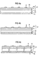
- the semiconductor body shown in FIG. 1 is a light-emitting semiconductor body, e.g. B. a light emitting diode semiconductor body.
- a light-emitting layer sequence 18 is arranged on a GaP substrate 1.
- a first GaAs x P 1-x epitaxial layer 2 with 0 x x ⁇ 1 is applied, over which in turn a second nAs-doped GaAs x P 1-x epitaxial layer 3 with 0 x x ⁇ 1 is arranged.
- Te or S can be used as the n-dopant.
- the underside of the GaP substrate 1 is provided with a first contact metallization 5, which consists, for example, of an Au-Ge alloy / Ag / Au layer sequence.
- a second contact metallization 6 is applied to the top of the third GaAs x P 1-x epitaxial layer 4.
- Any other combination of materials and layers known to the person skilled in the art to be suitable can also be used for the contact metallizations 5 and 6.
- the method for producing the roughening 8 consists of a first and a second etching step, the free surface 7 of the semiconductor body during the first etching step using an etching solution of the composition H 2 SO 4 : H 2 O 2 : H 2 O (3: 1: 1) and is treated with hydrofluoric acid (40 to 50%) in the second etching step.
- the first etching step is carried out at a temperature of between 15 and 80 °, especially 25 ° C and lasts between 30 seconds and 10 minutes.
- the second etching step is carried out at a temperature between 15 and 30 ° C and takes between 30 minutes and 120 minutes.
- the semiconductor body shown in Figure 2 also a Semiconductor body emitting light, in turn, has a GaP substrate 1 on. There is an n-doped first on the GaP substrate GaP: N epitaxial layer 9 applied, over which a p-doped second GaP: N epitaxial layer 10 is arranged.
- N-doping of GaP becomes a narrowing of the band gap reached, causing the GaP substrate to turn for that in layer sequence 17 from first 9 and second 10 GaP: N epitaxial layer generated light is transparent.
- FIG. 1 Another difference from the semiconductor body shown in FIG. 1 is that only the top 11 of the Semiconductor body is provided with a roughening 8 and the Side surfaces 12 are not roughened. That to make the roughening 8 used method corresponds for example the method explained in connection with Figure 1.
- FIG. 2 shows an example of how the Semiconductor body in a conventional LED housing a first 19 and a second 20 electrical connection, an opaque body 21 and one translucent envelope 22, may be installed.
- the semiconductor body is, for example, electrical conductive solder or adhesive with its first Contact metallization 5 on the second electrical connection 20 attached.
- the second contact metallization 6 is by means of a bonding wire 23 with the first electrical connection 19 connected.
- the base body 21 partially encloses the electrical Connections 19, 20 and has a recess in the semiconductor body is arranged.
- the recess is for example shaped so that it is for that of the semiconductor body decoupled light forms a reflector.
- HOT STUFF is the recess with the translucent envelope 22 filled directly to the free surface 7 of the semiconductor body borders.
- the envelope 22 is, for example made of a transparent synthetic resin and forms with the roughening 8 of the semiconductor body has a micro toothing from the adhesive strength of the cladding 22 on the semiconductor body increases and thus the risk of delamination
- the semiconductor body of Figure 1 in such a Housing can be installed.
- the micro toothing forms then of course not only on the top of the semiconductor body but also on the side surfaces.
- the housing can also be made in one piece from a transparent Be made of plastic and have any shape.
- the semiconductor body of FIG. 1 can of course also be used be manufactured in such a way that it is only on its top 11 has a roughening 8.
- the semiconductor body can likewise of Figure 2 over its entire free surface 7 with a Roughening 8 are provided.
- the semiconductor wafer consisting of the GaP substrate, the first 2, second 3 and third 4 GaAs x P 1-x epitaxial layer, the first 5 and the second 6 contact metallizations, is placed on a holding means 16, for example one Adhesive film, applied and separated into individual semiconductor bodies. This is done, for example, using saws.
- the finished, roughened semiconductor body can then be separated from the holding means 16 and for example processed into LEDs.
- the process sequence shown schematically in FIG simultaneous production of a plurality of semiconductor bodies 2 differs from that of FIG essentially in that the first and the second etching step is carried out before the semiconductor wafer is separated. This ensures that only a part, namely not part of the upper side covered by the contact metallizations 6 11 of the semiconductor wafer with a roughening 8 becomes.
Landscapes
- Engineering & Computer Science (AREA)
- Power Engineering (AREA)
- Microelectronics & Electronic Packaging (AREA)
- Computer Hardware Design (AREA)
- General Physics & Mathematics (AREA)
- Physics & Mathematics (AREA)
- Electromagnetism (AREA)
- Condensed Matter Physics & Semiconductors (AREA)
- Manufacturing & Machinery (AREA)
- Led Devices (AREA)
- Weting (AREA)
- Semiconductor Lasers (AREA)
- Photovoltaic Devices (AREA)
Abstract
Description
Die Erfindung bezieht sich auf ein Verfahren zum Herstellen eines Licht aussendenden und/oder empfangenden Halbleiterkörpers mit mindestens einer Halbleiterschicht, die aus GaAsxP1-x mit 0 ≤ x < 1 besteht.The invention relates to a method for producing a light-emitting and / or receiving semiconductor body with at least one semiconductor layer which consists of GaAs x P 1-x with 0 ≤ x <1.
Leuchtdioden mit derartigen Halbleiterkörpern sind bekannt. So ist beispielsweise in der europäischen Patentanmeldung EP 584 599 ein Leuchtdiodenchip beschrieben, bei dem auf einem n-leitenden GaP-Substrat eine n-leitende GaP-Epitaxieschicht und auf dieser eine p-leitende GaP-Epitaxieschicht aufgebracht ist. Die Unterseite des GaP-Substrats ist mit einer Kontaktmetallisierung aus einer Au-Ge-Legierung versehen und auf der Oberseite der p-leitenden GaP-Epitaxieschicht ist eine Kontaktmetallisierung aufgebracht, die sich ausgehend von der p-leitenden GaP-Epitaxieschicht beispielsweise aus einer Au-Schicht, einer Au-Zn-Schicht, einer Ti-W-N-Schicht und einer Au- oder Al-Schicht zusammensetzt.Light-emitting diodes with such semiconductor bodies are known. For example, in European patent application EP 584 599 describes a light-emitting diode chip in which on a n-type GaP substrate an n-type GaP epitaxial layer and applied a p-type GaP epitaxial layer thereon is. The bottom of the GaP substrate is with a Contact metallization made of an Au-Ge alloy and on the top of the p-type GaP epitaxial layer applied a contact metallization, starting out from the p-type GaP epitaxial layer, for example an Au layer, an Au-Zn layer, a Ti-W-N layer and an Au or Al layer.
Weiterhin sind Leuchtdioden bekannt, bei denen auf einem GaP-Substrat mittels Epitaxie eine Schichtenfolge aus GaAsP aufgebracht ist. Diese Schichtenfolge weist beispielsweise ausgehend vom GaP-Substrat zunächst eine GaAsP-Übergangsschicht mit zunehmendem As-Gehalt, eine n-dotierte GaAsP-Schicht (Dotierstoff: z. b. Tellur oder Schwefel) und eine p-dotierte GaAsP-Schicht (Dotierstoff: Zink) auf. Auf die p-dotierte GaAsP-Schicht ist eine Kontaktmetallisierung aufgebracht, die beispielsweise ausgehend von der p-dotierten GaAsP-Schicht aus einer Gold-Zink-Schicht, einer TiWN-Schicht und einer Aluminium-Schicht besteht. Die Unterseite des GaP-Substrats ist mit einer Kontaktmetallisierung versehen, die beispielsweise aus einer auf dem GaP-Substrat aufgebrachten Gold-Germanium-Schicht besteht.Furthermore, light-emitting diodes are known in which on a GaP substrate a layer sequence of GaAsP is applied by means of epitaxy is. This layer sequence points out, for example a GaAsP transition layer from the GaP substrate with increasing As content, an n-doped GaAsP layer (Dopant: e.g. tellurium or sulfur) and a p-doped GaAsP layer (dopant: zinc). On the p-doped GaAsP layer is applied to a contact metallization for example, starting from the p-doped GaAsP layer a gold-zinc layer, a TiWN layer and one There is an aluminum layer. The bottom of the GaP substrate is provided with a contact metallization, for example from a gold germanium layer applied to the GaP substrate consists.
Je nach As-Gehalt kann mit einem oben beschriebenen Halbleiterkörper eine Leuchtdiode hergestellt werden, die Licht aus dem Bereich Gelb bis Superrot aussendet. Der Nachteil dieser Halbleiterkörper besteht jedoch darin, daß das im Halbleiterkörper erzeugte Licht nur zu einem Bruchteil aus dem Halbleiterkörper ausgekoppelt wird.Depending on the As content, a semiconductor body described above can be used A light emitting diode can be made to emit light the range from yellow to super red. The disadvantage of this Semiconductor body, however, is that in the semiconductor body only a fraction of the light generated from the semiconductor body is decoupled.
In der US-Patentschrift 4,582,952 ist eine Solarzelle beschrieben, die, ausgehend von einem transparenten GaP-Substrat, aus einer ersten p-dotierten GaAsP-Schicht mit abgestuftem As-Gehalt, aus einer zweiten p-dotierten GaAsP-Schicht, aus einer n-dotierten GaAsP-Schicht und aus einer GaP-Abdeckschicht aufgebaut ist. Das GaP-Substrat und die GaP-Abdeckschicht sind jeweils mit einer Mehrzahl von Metallkontakten versehen.A solar cell is described in US Pat. No. 4,582,952, which, based on a transparent GaP substrate, from a first p-doped GaAsP layer with graded As content, from a second p-doped GaAsP layer, from an n-doped GaAsP layer and from one GaP cover layer is built up. The GaP substrate and the GaP cover layers are each with a plurality of metal contacts Mistake.
Der Wirkungsgrad einer lichtemittierenden Diode bzw. einer Photodiode oder Solarzelle wird zu einem wesentlichen Anteil von den beim Austreten bzw. Eintreten der Strahlung aus bzw. in den Halbleiterkörper auftretenden Verlusten bestimmt. Eine Hauptursache für diese Verluste ist der große Unterschied der Brechungsindices von Halbleitermaterial und angrenzendem Medium (z. B. Luft oder Kunststoffumhüllung). Dieser große Unterschied bewirkt einen sehr kleinen Grenzwinkel der Totalreflexion für den Durchtritt der Strahlung durch die Oberfläche des Halbleiterkörpers. Auf direktem Wege tritt aber nur derjenige Strahlungsanteil aus dem Halbleiterkörper aus, welcher unter einem kleineren Winkel zur Oberflächenormalen als der Grenzwinkel auf die Grenzfläche fällt. Der verbleibende Strahlungsanteil wird in den Halbleiterkörper zurückreflektiert. Aus US-A-5 429 954 ist ein Verfahren zum Herstellen einer lichtemittierende Diode mit einer durch Ätzen erzeugten Oberflächenaufrauhung bekannt. EP-A-0 198 199 beschreibt ein Verfahren zur Herstellung eine Oberflächengitters auf der Oberfläche eines Halbleitersubstrats aus GaAs mittels einer Ätzlösung aus Schwefelsäure, Wasserstoffperoxid und Wasser. The efficiency of a light emitting diode Photodiode or solar cell becomes an essential part from those when the radiation emerges or enters losses occurring in the semiconductor body determined. A The main cause of these losses is the big difference in the Refractive index of semiconductor material and adjacent medium (e.g. air or plastic wrapping). That big difference causes a very small critical angle of total reflection for the passage of the radiation through the surface of the semiconductor body. But only the one steps directly Radiation component from the semiconductor body, which at a smaller angle to the surface normal than that Limit angle falls on the interface. The remaining one Radiation component is reflected back into the semiconductor body. From US-A-5 429 954 is a method of making a light emitting diode with an etching generated Surface roughening known. EP-A-0 198 199 describes a Process for producing a surface grid on the surface of a Semiconductor substrates made of GaAs using an etching solution made of sulfuric acid, Hydrogen peroxide and water.
Die Aufgabe der Erfindung besteht darin, ein Verfahren zum Herstellen eines Licht aussendenden und/oder empfangenden Halbleiterkörpers mit mindestens einer Halbleiterschicht aus GaAsxP1-x mit 0 ≤ x < 1 zu entwickeln, der eine verbesserte Lichtaus- bzw. -einkoppelung aufweist.The object of the invention is to develop a method for producing a light-emitting and / or receiving semiconductor body with at least one semiconductor layer made of GaAs x P 1-x with 0 x x <1, which has an improved coupling in and out of light.
Diese Aufgabe wird durch ein Verfahren mit den Merkmalen des
Anspruches 1 gelöst. Vorteilhafte Weiterbildungen des erfindungsgemäßen
Verfahrens sind Gegenstand der Unteransprüche 2
bis 9.This task is accomplished by a process with the characteristics of
Claim 1 solved. Advantageous further developments of the invention
Procedures are the subject of
Erfindungsgemäß ist vorgesehen, daß zumindest ein Teil der Oberfläche der Halbleiterschicht in einem ersten Ätzschritt mit einer Ätzlösung der Zusammensetzung H2SO4:H2O2:H2O und nachfolgend in einem zweiten Ätzschritt mit verdünnter Flußsäure behandelt wird, so daß zumindest auf einem Teil der Oberfläche der Halbleiterschicht eine Aufrauhung erzeugt wird.According to the invention it is provided that at least part of the surface of the semiconductor layer is treated in a first etching step with an etching solution of the composition H 2 SO 4 : H 2 O 2 : H 2 O and subsequently in a second etching step with dilute hydrofluoric acid, so that at least part of the surface of the semiconductor layer is roughened.
Durch die Aufrauhung der Oberfläche wird vorteilhafterweise erreicht, daß im Vergleich zu einer ebenen Oberfläche ein größerer Anteil der in dem Halbleiterkörper erzeugten Strahlung in einem Winkel auf die Oberfläche der Halbleiterschicht trifft, der kleiner als der Grenzwinkel der Totalreflexion ist.The surface is advantageously roughened achieved that compared to a flat surface greater proportion of the radiation generated in the semiconductor body at an angle to the surface of the semiconductor layer that is smaller than the critical angle of total reflection is.
Ein weiterer Vorteil der aufgerauhten Halbleiteroberfläche besteht darin, daß bei einem Halbleiterbauelement, bei dem ein Halbleiterkörper unmittelbar von einer Kunststoffumhüllung umgeben ist, eine erhöhte Haftfestigkeit zwischen dem Halbleiterkörper und der Kunststoffumhüllung erzielt wird. Dadurch ist die Gefahr einer Ablösung der Kunststoffumhüllung vom Halbleiterkörper während des Betriebes und eine demzufolge beschleunigte Alterung des Halbleiterbauelements verringert. Another advantage of the roughened semiconductor surface is that in a semiconductor device in which a semiconductor body directly from a plastic coating is surrounded, an increased adhesive strength between the Semiconductor body and the plastic coating is achieved. This creates the danger of the plastic covering becoming detached from the semiconductor body during operation and consequently accelerated aging of the semiconductor device is reduced.
Gemäß einer vorteilhaften Weiterbildung des erfindungsgemäßen Verfahrens wird bei einem Halbleiterkörper mit einem n-dotierten GaP-Substrat, auf dem eine Schichtenfolge aus GaAsP aufgebracht ist, die gesamte freie Oberfläche des Halbleiterkörpers aufgerauht. Unter freier Oberfläche ist hier der Teilbereich der Oberfläche zu verstehen, der nicht mit einer Kontaktmetallisierungsschicht versehen ist.According to an advantageous development of the invention The method is used for a semiconductor body with an n-doped GaP substrate on which a layer sequence of GaAsP is applied, the entire free surface of the semiconductor body roughened. Here is the free surface Part of the surface to understand that not with a Contact metallization layer is provided.
Bei Leuchdioden mit einem derartigen zur Lichterzeugung geeigneten Halbleiterkörper ist das GaP-Substrat für die in der GaAsP-Schichtenfolge erzeugte elektromagnetische Strahlung durchlässig, da der Bandabstand von GaAsP kleiner ist als der von GaP. Daher kann vorteilhafterweise die Strahlung durch die gesamte freie Oberfläche des Halbleiterkörpers hindurch aus diesem ausgekoppelt werden.In the case of light-emitting diodes with a suitable one for generating light Semiconductor body is the GaP substrate for the in the GaAsP layer sequence generated electromagnetic radiation permeable because the band gap of GaAsP is smaller than that by GaP. Therefore, the radiation can advantageously pass through the entire free surface of the semiconductor body be coupled out of this.
Vorteilhafterweise weist eine auf eine Unterseite des GaP-Substrats aufgebrachte Kontaktmetallisierung an der Grenze zum Halbleiterkörper eine Spiegelfläche auf. Dies hat zur Folge, daß die von der GaAsP-Schichtenfolge in Richtung der Kontaktmetallisierung ausgesandte Strahlung von dieser weitgehend reflektiert wird und nachfolgend durch die freie Oberfläche ausgekoppelt werden kann.One advantageously has an underside of the GaP substrate applied contact metallization at the border a mirror surface to the semiconductor body. This has to Consequence that of the GaAsP layer sequence in the direction of Contact metallization radiation emitted by this largely is reflected and subsequently by the free surface can be coupled out.
Bei einer bevorzugten Weiterbildung des erfindungsgemäßen Verfahrens, wird beim ersten Ätzschritt für die Ätzlösung H2SO4:H2O2:H2O ein Verhältnis von 3:1:1, eine Temperatur zwischen 20 und 80° und eine Ätzdauer zwischen einer halben Minute und 10 Minuten gewählt. Mit dieser Maßnahme wird u. a. erreicht, daß die zu ätzende Oberfläche des Halbleiterkörpers vollständig von Verschmutzungen und anderen Rückständen befreit wird. In a preferred development of the method according to the invention, in the first etching step for the etching solution H 2 SO 4 : H 2 O 2 : H 2 O, a ratio of 3: 1: 1, a temperature between 20 and 80 ° and an etching time between half Minute and 10 minutes selected. With this measure it is achieved, inter alia, that the surface of the semiconductor body to be etched is completely freed of dirt and other residues.
Bei einer weiteren bevorzugten Weiterbildung des erfindungsgemäßen Verfahrens und dessen Weiterbildungen wird beim zweiten Ätzschritt eine 40-50%ige Flußsäure verwendet. Der zweite Ätzschritt wird bei einer Temperatur zwischen 15 und 30°, insbesondere bei ca. 25° durchgeführt und dauert zwischen 30 Minuten und 120 Minuten.In a further preferred development of the invention The procedure and its training will be the second Etching step uses a 40-50% hydrofluoric acid. The second Etching step is carried out at a temperature between 15 and 30 °, performed especially at approx. 25 ° and lasts between 30 Minutes and 120 minutes.
Mittels der beiden oben angegebenen Ätzschritte wird vorteilhafter Weise eine Oberflächenaufrauhung erzielt, die die Gestalt von nebeneinander angeordneten Sägezähnen mit einer Höhe von ca. 1 µm aufweist. Bei Leuchtdioden kann dadurch vorteilhafterweise eine Lichtsteigerung von ca. 40% erzielt werden.By means of the two etching steps specified above, it becomes more advantageous Way a surface roughening achieved the shape of saw teeth arranged side by side with a Has a height of about 1 µm. With LEDs, this can advantageously achieved a light increase of approximately 40% become.
Bei einer anderen bevorzugten Weiterbildung des erfindungsgemäßen Verfahrens weist der Halbleiterkörper ein GaP-Substrat auf, auf dem eine Schichtenfolge aus Stickstoff(N)-dotiertem GaP (kurz: GaP:N) aufgebracht ist. Auch bei einem derartigen zur Lichterzeugung geeigneten Halbleiterkörper ist vorteilhafterweise das Substrat für die in der GaP-Schichtenfolge erzeugte Strahlung durchlässig, so daß auch hier durch die Aufrauhung der Halbleiteroberfläche eine wesentliche Steigerung der Lichtauskoppelung erzielt wird.In another preferred development of the invention In the method, the semiconductor body has a GaP substrate on which a layer sequence of nitrogen (N) -doped GaP (short: GaP: N) is applied. Even with such a semiconductor body suitable for light generation is advantageous the substrate for that in the GaP layer sequence generated radiation permeable, so that here too by the Roughening the semiconductor surface a significant increase the light decoupling is achieved.
Bei einem besonders vorteilhaften Verfahren zum gleichzeitigen Herstellen einer Mehrzahl von Halbleiterkörpern der eingangs genannten Art wird zunächst auf einer Substratscheibe aus GaP eine Schichtenfolge aus GaAsxP1-x mit 0 ≤ x < 1 oder GaP:N aufgebracht. Nachfolgend wird auf die Unterseite der Substratscheibe eine erste Kontaktmetallisierung und auf die Oberseite der Schichtenfolge eine Mehrzahl von zweiten Kontaktmetallisierungen aufgebracht. Anschließend wir die freie Oberfläche der Schichtenfolge zunächst in einem ersten Ätzschritt mit der Ätzlösung der Zusammensetzung H2SO4:H2O2:H2O und in einem zweiten Ätzschritt mit Flußsäure (HF) behandelt. In a particularly advantageous method for the simultaneous production of a plurality of semiconductor bodies of the type mentioned at the outset, a layer sequence of GaAs x P 1-x with 0 x x <1 or GaP: N is first applied to a substrate wafer made of GaP. A first contact metallization is then applied to the underside of the substrate wafer and a plurality of second contact metallizations are applied to the top of the layer sequence. Then the free surface of the layer sequence is first treated in a first etching step with the etching solution of the composition H 2 SO 4 : H 2 O 2 : H 2 O and in a second etching step with hydrofluoric acid (HF).
Abschließend wird die Halbleiterscheibe, bestehend aus Substratscheibe, Schichtenfolge, erster und zweiten Kontaktmetallisierungen zu einzelnen Halbleiterkörpern, z. B. Leuchtdiodenchips, vereinzelt.Finally, the semiconductor wafer consisting of Substrate wafer, layer sequence, first and second contact metallizations to individual semiconductor bodies, e.g. B. LED chips, isolated.
ist vorgesehen, daß auch die Seitenflächen der Halbleiterkörper aufgerauht werden, so wird die Halbleiterscheibe nach dem Aufbringen der ersten und zweiten Kontaktmetallisierungen zum Beispiel auf eine Klebefolie oder ein anderes Haltemittel aufgebracht und in einzelne Leuchtdioden-Halbleiterkörper vereinzelt. Anschließend werden die beiden oben genannten Ätzschritte durchgeführt, bevor dann die vereinzelten Halbleiterkörper von dem Haltemittel abgehoben und z. B. zu Leuchtdioden weiterverarbeitet werden.it is provided that the side faces of the semiconductor body be roughened, the semiconductor wafer after the Application of the first and second contact metallizations for Example on an adhesive film or another holding device applied and in individual light emitting diode semiconductor body sporadically. Then the two above Etching steps are carried out before the isolated semiconductor body lifted off the holding means and z. B. too LEDs are processed further.
Das erfindungsgemäße Verfahren wird nun anhand von Ausführungsbeispielen
in Verbindung mit den Figuren 1 bis 4 näher
erläutert. Es zeigen:
In den Figuren sind gleiche Teile immer mit denselben Bezugszeichen versehen. In the figures, the same parts are always given the same reference numerals Mistake.
Bei dem in Figur 1 dargestellten Halbleiterkörper handelt es
sich um einen Licht aussendenden Halbleiterkörper, z. B. um
einen Leuchtdioden-Halbleiterkörper. Hierbei ist auf einem
GaP-Substrats 1 eine Licht aussendende Schichtenfolge 18 angeordnet.
Auf dem GaP-Substrat 1 ist beispielsweise eine erste
GaAsxP1-x-Epitaxieschicht 2 mit 0 ≤ x < 1 aufgebracht,
über der wiederum eine beispielsweise n-dotierte zweite
GaAsxP1-x-Epitaxieschicht 3 mit 0 ≤ x < 1 angeordnet ist. Als
n-Dotierstoff kann beispielsweise Te oder S verwendet sein.The semiconductor body shown in FIG. 1 is a light-emitting semiconductor body, e.g. B. a light emitting diode semiconductor body. Here, a light-emitting
Auf der zweiten GaAsxP1-x-Epitaxieschicht 3 ist eine z. B. p-dotierte
dritte GaAsxP1-x-Epitaxieschicht 4 mit 0 ≤ x < 1 aufgebracht,
die beispielsweise mit Zn dotiert ist. Die erste
GaAsxP1-x-Epitaxieschicht 2 weist ausgehend vom GaP-Substrat 1
einen zunehmenden As-Gehalt auf, z. B. von x = 0 bis x = As-Gehalt
der zweiten GaAsxP1-x-Epitaxieschicht 4.On the second GaAs x P 1-x epitaxial layer 3 a z. B. p-doped third GaAs x P 1-x
Die Unterseite des GaP-Substrats 1 ist mit einer ersten Kontaktmetallisierung
5 versehen, die beispielsweise aus einer
Schichtenfolge Au-Ge-Legierung/Ag/Au besteht. Auf der Oberseite
der dritten GaAsxP1-x-Epitaxieschicht 4 ist eine zweite
Kontaktmetallisierung 6 aufgebracht. Diese weist z. B. eine
unmittelbar auf die dritte GaAsxP1-x-Epitaxieschicht 4 aufgebrachten
Au-Zn-Schicht und eine auf dieser aufgebrachten Au-Schicht
auf. Für die Kontaktmetallisierungen 5 und 6 kann
aber auch jede andere dem Fachmann als geeignet bekannte Material-
und Schichtenkombination verwendet werden.The underside of the GaP substrate 1 is provided with a
Die gesamte freie Oberfläche 7, d. h. die nicht von der ersten
5 und zweiten 6 Kontaktmetallisierung abgedeckten Oberfläche
des Halbleiterkörpers, in diesem Falls ist dies ein
Teil der Oberseite 11 und die Seitenflächen 12, ist mit einer
Aufrauhung 8 versehen. Diese weist eine Struktur von nebeneinander
angeordneten Sägezähnen (Höhe z. B. ca. 1 µm) auf. The entire
Das Verfahren zum Herstellen der Aufrauhung 8 besteht aus einem
ersten und zweiten Ätzschritt, wobei die freie Oberfläche
7 des Halbleiterkörpers beim ersten Ätzschritt mit einer Ätzlösung
der Zusammensetzung H2SO4:H2O2:H2O (3:1:1) und beim
zweiten Ätzschritt mit Flußsäure (40 bis 50%) behandelt wird.The method for producing the
Der erste Ätzschritt wird bei einer Temperatur von zwischen 15 und 80°, insbesondere 25°C durchgeführt und dauert zwischen 30 Sekunden und 10 Minuten. Der zweite Ätzschritt wird bei einer Temperatur zwischen 15 und 30°C durchgeführt und dauert zwischen 30 Minuten und 120 Minuten.The first etching step is carried out at a temperature of between 15 and 80 °, especially 25 ° C and lasts between 30 seconds and 10 minutes. The second etching step is carried out at a temperature between 15 and 30 ° C and takes between 30 minutes and 120 minutes.
Der in Figur 2 dargestellte Halbleiterkörper, ebenfalls ein
Licht aussendender Halbleiterkörper, weist wiederum ein GaP-Substrat
1 auf. Auf dem GaP-Substrat ist eine n-dotierte erste
GaP:N-Epitaxieschicht 9 aufgebracht, über der eine p-dotierte
zweite GaP:N-Epitaxieschicht 10 angeordnet ist. Durch
die N-Dotierung von GaP wird eine Verkleinerung der Bandlücke
erreicht, wodurch bewirkt ist, daß das GaP-Substrat wiederum
für das in der Schichtenfolge 17 aus erster 9 und zweiter 10
GaP:N-Epitaxieschicht erzeugte Licht transparent ist.The semiconductor body shown in Figure 2, also a
Semiconductor body emitting light, in turn, has a GaP substrate
1 on. There is an n-doped first on the GaP substrate
GaP:
Ein weiterer Unterschied zu dem in Figur 1 gezeigten Halbleiterkörper
besteht darin, daß hier nur die Oberseite 11 des
Halbleiterkörpers mit einer Aufrauhung 8 versehen ist und die
Seitenflächen 12 nicht aufgerauht sind. Das zum Herstellen
der Aufrauhung 8 eingesetzte Verfahren entspricht beispielsweise
dem in Verbindung mit Figur 1 erläuterten Verfahren.Another difference from the semiconductor body shown in FIG. 1
is that only the top 11 of the
Semiconductor body is provided with a
Weiterhin ist in Figur 2 beispielhaft dargestellt, wie der
Halbleiterkörper in ein herkömmliches LED-Gehäuse, bestehend
aus einem ersten 19 und einem zweiten 20 elektrischen Anschluß,
einem lichtundurchlässigen Grundkörper 21 und einer
lichtdurchlässigen Umhüllung 22, eingebaut sein kann. Hierbei
ist der Halbleiterkörper beispielsweise mittels eines elektrisch
leitenden Lotes oder Klebstoffes mit seiner ersten
Kontaktmetallisierung 5 auf dem zweiten elektrischen Anschluß
20 befestigt. Die zweite Kontaktmetallisierung 6 ist mittels
eines Bonddrahtes 23 mit dem ersten elektrischen Anschluß 19
verbunden. Der Grundkörper 21 umschließt teilweise die elektrischen
Anschlüsse 19,20 und weist eine Ausnehmung auf, in
der der Halbleiterkörper angeordnet ist. Die Ausnehmung ist
beispielsweise derart geformt, daß sie für das von dem Halbleiterkörper
ausgekoppelte Licht einen Reflektor bildet. Auβerdem
ist die Ausnehmung mit der lichtdurchlässigen Umhüllung
22 gefüllt, die unmittelbar an die freie Oberfläche 7
des Halbleiterkörpers grenzt. Die Umhüllung 22 besteht beispielsweise
aus einem transparenten Kunstharz und bildet mit
der Aufrauhung 8 des Halbleiterkörpers eine Mikroverzahnung
aus, die die Haftfestigkeit der Umhüllung 22 auf dem Halbleiterkörper
erhöht und damit die Gefahr einer Delamination
deutlich senkt.Furthermore, FIG. 2 shows an example of how the
Semiconductor body in a conventional LED housing
a first 19 and a second 20 electrical connection,
an
Der Vollständigkeit halber sei erwähnt, daß selbstverständlich auch der Halbleiterkörper von Figur 1 in ein derartiges Gehäuse eingebaut werden kann. Die Mikroverzahnung bildet sich dann natürlich nicht nur an der Oberseite des Halbleiterkörpers sondern auch an dessen Seitenflächen aus. Ebenso kann das Gehäuse auch einstückig aus einem transparenten Kunststoff gefertigt sein und eine beliebige Form aufweisen.For the sake of completeness, it goes without saying also the semiconductor body of Figure 1 in such a Housing can be installed. The micro toothing forms then of course not only on the top of the semiconductor body but also on the side surfaces. As well the housing can also be made in one piece from a transparent Be made of plastic and have any shape.
Durch das Aufrauhen der freien Oberfläche der Halbleiterkörper wird beispielsweise bei Leuchtdioden, die mit den oben beschriebenen Halbleiterkörpern versehen sind, eine Lichtsteigerung von mehr als 40% erzielt.By roughening the free surface of the semiconductor body is used, for example, with LEDs that match the above described semiconductor bodies are provided, an increase in light achieved by more than 40%.
Selbstverständlich kann auch der Halbleiterkörper von Figur 1
derart hergestellt werden, daß er nur auf seiner Oberseite 11
eine Aufrauhung 8 aufweist. Ebenso kann der Halbleiterkörper
von Figur 2 über seine gesamte freie Oberfläche 7 mit einer
Aufrauhung 8 versehen werden.The semiconductor body of FIG. 1 can of course also be used
be manufactured in such a way that it is only on its top 11
has a
Bei dem in Figur 3 schematisch dargestellten Verfahrensablauf
zum gleichzeitigen Herstellen einer Mehrzahl von Halbleiterkörpern
gemäß Figur 1 wird zunächst (Teilbild A) auf eine
vorgefertigte GaP-Substratscheibe 13 die erste GaAsxP1-x-Epitaxieschicht
2, die zweite GaAsxP1-x-Epitaxieschicht 3 und die
dritte GaAsxP1-x-Epitaxieschicht 4 aufgebracht. Die Unterseite
14 der Substratscheibe 13 wird mit der Kontaktmetallisierung
5 versehen. Auf die Oberseite 15 der dritten GaAsxP1-x-Epitaxieschicht
4 wird eine Mehrzahl von zweiten Kontaktmetallisierungen
6 aufgebracht. Die Kontaktmetallisierungen 5,6 werden
beispielsweise mittels Aufdampfen oder Sputtern hergestellt.In the process sequence schematically shown in FIG. 3 for the simultaneous production of a plurality of semiconductor bodies according to FIG. 1, first (partial image A) the first GaAs x P 1 -
Anschließend (Teilbild B) wird die Halbleiterscheibe, bestehend aus dem GaP-Substrat, der ersten 2, zweiten 3 und dritten 4 GaAsxP1-x-Epitaxieschicht, der ersten 5 und den zweiten 6 Kontaktmetallisierungen, auf ein Haltemittel 16, beispielsweise eine Klebefolie, aufgebracht und in einzelne Halbleiterkörper vereinzelt. Dies erfolgt beispielsweise mittels Sägen.Subsequently (partial image B), the semiconductor wafer, consisting of the GaP substrate, the first 2, second 3 and third 4 GaAs x P 1-x epitaxial layer, the first 5 and the second 6 contact metallizations, is placed on a holding means 16, for example one Adhesive film, applied and separated into individual semiconductor bodies. This is done, for example, using saws.
Nachfolgend (Teilbild C) werden dann die freien Oberflächen, also jeweils ein Teil der Oberseite 11 und die Seitenflächen 12 (Schnittflanken) der Halbleiterkörper, wie weiter oben erläutert, mittels dem ersten und dem zweiten Ätzschritt aufgerauht. Die fertiggestellten, aufgerauhten Halbleiterkörper können dann von dem Haltemittel 16 abgetrennt und beispielsweise zu Leuchtdioden weiterverarbeitet werden.The free surfaces, So part of the top 11 and the side surfaces 12 (cut edges) of the semiconductor body, as explained above, roughened by means of the first and the second etching step. The finished, roughened semiconductor body can then be separated from the holding means 16 and for example processed into LEDs.
Der in Figur 4 schematisch dargestellte Verfahrensablauf zum
gleichzeitigen Herstellen einer Mehrzahl von Halbleiterkörpern
gemäß Figur 2 unterscheidet sich von dem von Figur 3 im
wesentlichen dadurch, daß der erste und der zweite Ätzschritt
vor dem Vereinzeln der Halbleiterscheibe durchgeführt wird.
Dadurch wird erreicht, daß nur ein Teil, nämlich der nicht
von den Kontaktmetallisierungen 6 abgedeckte Teil der Oberseite
11 der Halbleiterscheibe mit einer Aufrauhung 8 versehen
wird.The process sequence shown schematically in FIG
simultaneous production of a plurality of
Ebenso kann vorgesehen sein, daß nur die Oberseite 11 und
Teilbereiche der Seitenflächen 12 der Halbleiterkörper eine
Aufrauhung 8 aufweisen. In diesem Fall wird die Halbleiterscheibe
vor den Ätzschritten nicht vollständig durchsägt sondern
nur angesägt und erst nach dem Ätzen vereinzelt.It can also be provided that only the top 11 and
Partial areas of the side surfaces 12 of the semiconductor body a
Wird für die zweiten Kontaktmetallisierungen 6 ein Material
verwendet, das bei einem der beiden Ätzschritte angegriffen
würde, so können diese vorher mit einer gegen die Ätzlösung
resistenten Abdeckschicht abgedeckt werden. Diese Abdeckschicht
wird nach dem Aufrauhen dann wieder entfernt.Becomes a material for the
Claims (9)
- Process for producing a light-emitting and/or - receiving semiconductor body having at least one semiconductor layer composed of GaAsxP1-x, where 0 ≤ X < 1, characterized in that at least one part of the surface of the semiconductor layer is treated with an etching solution having the composition H2SO4:H2O2:H2O in a first etching step and then with hydrofluoric acid in a second etching step, with the result that a roughness (8) is produced at least on the part of the surface of the semiconductor layer.
- Process according to Claim 1, characterized in that the roughness (8) has the shape of saw teeth which are arranged next to one another.
- Process according to Claim 1 or 2, characterized in that use is made of a semiconductor body with a GaP substrate on which is applied a layer sequence (17,18) having at least one nitrogen-doped GaP epitaxial layer.
- Process according to Claim 1 or 2, characterized in that use is made of a semiconductor body with a GaP substrate on which is applied a layer sequence (17,18) having at least one GaAsxP1-x epitaxial layer, where 0 < x < 1.
- Process according to one of Claims 1 to 4, characterized in that the entire free surface (7) of the semiconductor body has the roughness (8).
- Process for simultaneously producing a plurality of light-emitting and/or -receiving semiconductor bodies having at least one semiconductor layer which is composed of GaAsxP1-x, where 0 ≤ x < 1, or of GaP:N which comprises the following steps:a) a layer sequence (17,18) made of GaAsxP1-x, where 0 ≤ x < 1 is firstly applied to a substrate wafer (13) made of GaP,b) a first contact metallization layer (5) is applied to the underside (14) of the substrate wafer (13) and at least one second contact metallization layer (6) is applied to the top side (15) of the layer sequence (17,18),c) the free surface of the layer sequence (17,18) is firstly treated with an etching solution having the composition H2SO4:H2O2:H2O in a first etching step and with hydrofluoric acid (HF) in a second etching step, with the result that a roughness (8) of the free surface is produced, andd) the semiconductor wafer, comprising the substrate wafer (13), the layer sequence (17,18), the first (5) and the second (6) contact metallization layers, is separated to form individual semiconductor bodies.
- Process for simultaneously producing a plurality of light-emitting and/or -receiving semiconductor bodies having at least one semiconductor layer which is composed of GaAsxP1-x, where 0 ≤ x < 1, or of GaP:N, which comprises the following steps:a) a layer sequence (17,18) made of GaAsxP1-x, where 0 ≤ x < 1 is firstly applied to a substrate wafer (13) made of GaP,b) a first contact metallization layer (5) is applied to the underside (14) of the substrate wafer (13) and a plurality of second contact metallization layers (6) are applied to the top side (15) of the layer sequence (17,18),c) the semiconductor wafer, comprising the substrate wafer (13), the layer sequence (17,18), the first (5) and the second (6) contact metallization layers, is placed on a holding means (16),d) the semiconductor wafer is separated to form individual semiconductor bodies, ande) the free surfaces of the semiconductor bodies are firstly treated with an etching solution having the composition H2SO4:H2O2:H2O in a first etching step and with hydrofluoric acid (HF) in a second etching step, with the result that a roughness (8) of the surfaces is produced.
- Process according to one of Claims 1 to 7, characterized in that, in the case of the first etching step, a ratio of 3:1:1 is chosen for the etching solution H2SO4:H2O2:H2O, a temperature of between 15 and 80°C is chosen and an etching duration of between half a minute and 10 minutes is chosen.
- Process according to one of Claims 1 to 8, characterized in that, in the case of the second etching step, hydrofluoric acid with a concentration of 40-50% is chosen, a temperature of between 15 and 30°C is chosen and an etching duration of between 30 minutes and 120 minutes is chosen.
Applications Claiming Priority (3)
| Application Number | Priority Date | Filing Date | Title |
|---|---|---|---|
| DE19632627 | 1996-08-13 | ||
| DE19632627A DE19632627A1 (en) | 1996-08-13 | 1996-08-13 | Method for producing a light-emitting and / or receiving semiconductor body |
| PCT/DE1997/001729 WO1998007195A1 (en) | 1996-08-13 | 1997-08-13 | Process for producing a light-emitting and/or light-receiving semiconductor body |
Publications (2)
| Publication Number | Publication Date |
|---|---|
| EP0944924A1 EP0944924A1 (en) | 1999-09-29 |
| EP0944924B1 true EP0944924B1 (en) | 2002-10-23 |
Family
ID=7802534
Family Applications (1)
| Application Number | Title | Priority Date | Filing Date |
|---|---|---|---|
| EP97918885A Expired - Lifetime EP0944924B1 (en) | 1996-08-13 | 1997-08-13 | Process for producing a light-emitting and/or light-receiving semiconductor body |
Country Status (7)
| Country | Link |
|---|---|
| US (1) | US6531405B1 (en) |
| EP (1) | EP0944924B1 (en) |
| JP (1) | JP2001501365A (en) |
| CN (1) | CN1227748C (en) |
| DE (2) | DE19632627A1 (en) |
| TW (1) | TW353237B (en) |
| WO (1) | WO1998007195A1 (en) |
Families Citing this family (33)
| Publication number | Priority date | Publication date | Assignee | Title |
|---|---|---|---|---|
| EP2276075A1 (en) | 2000-02-15 | 2011-01-19 | OSRAM Opto Semiconductors GmbH | Radiation emitting semiconductor device and method for its production |
| DE10006738C2 (en) | 2000-02-15 | 2002-01-17 | Osram Opto Semiconductors Gmbh | Light-emitting component with improved light decoupling and method for its production |
| US6791119B2 (en) * | 2001-02-01 | 2004-09-14 | Cree, Inc. | Light emitting diodes including modifications for light extraction |
| US6909162B2 (en) * | 2001-11-02 | 2005-06-21 | Omnivision Technologies, Inc. | Surface passivation to reduce dark current in a CMOS image sensor |
| US6462365B1 (en) * | 2001-11-06 | 2002-10-08 | Omnivision Technologies, Inc. | Active pixel having reduced dark current in a CMOS image sensor |
| TW576864B (en) * | 2001-12-28 | 2004-02-21 | Toshiba Corp | Method for manufacturing a light-emitting device |
| JP3715627B2 (en) * | 2002-01-29 | 2005-11-09 | 株式会社東芝 | Semiconductor light emitting device and manufacturing method thereof |
| DE10203809B4 (en) * | 2002-01-31 | 2010-05-27 | Osram Opto Semiconductors Gmbh | Radiation-emitting semiconductor component |
| JP3705791B2 (en) | 2002-03-14 | 2005-10-12 | 株式会社東芝 | Semiconductor light emitting element and semiconductor light emitting device |
| JP3776824B2 (en) * | 2002-04-05 | 2006-05-17 | 株式会社東芝 | Semiconductor light emitting device and manufacturing method thereof |
| DE10229231B9 (en) * | 2002-06-28 | 2006-05-11 | Osram Opto Semiconductors Gmbh | A method of manufacturing a radiation emitting and / or receiving semiconductor chip having a radiation input and / or output microstructure |
| DE10324909B4 (en) * | 2003-05-30 | 2017-09-07 | Osram Opto Semiconductors Gmbh | Housing for a radiation-emitting component, method for its production and radiation-emitting component |
| JP4315744B2 (en) * | 2003-06-25 | 2009-08-19 | 株式会社沖データ | LAMINATE AND SEMICONDUCTOR DEVICE MANUFACTURING METHOD |
| TW200505042A (en) * | 2003-07-17 | 2005-02-01 | South Epitaxy Corp | LED device |
| US8237045B2 (en) * | 2004-03-12 | 2012-08-07 | Kyosemi Corporation | Laminated solar battery |
| WO2005091389A1 (en) * | 2004-03-19 | 2005-09-29 | Showa Denko K.K. | Compound semiconductor light-emitting device and production method thereof |
| JP4092658B2 (en) * | 2004-04-27 | 2008-05-28 | 信越半導体株式会社 | Method for manufacturing light emitting device |
| JP4692072B2 (en) * | 2005-05-19 | 2011-06-01 | 三菱化学株式会社 | Manufacturing method of light emitting diode |
| KR101154744B1 (en) * | 2005-08-01 | 2012-06-08 | 엘지이노텍 주식회사 | Nitride light emitting device and fabrication method thereof |
| TWI396307B (en) * | 2009-02-05 | 2013-05-11 | Huga Optotech Inc | Light-emitting diode |
| TWI470823B (en) | 2009-02-11 | 2015-01-21 | Epistar Corp | Light-emitting device and manufacturing method thereof |
| TWI408832B (en) * | 2009-03-30 | 2013-09-11 | Huga Optotech Inc | Light emitting device having pillar structure with hollow structure and the forming method thereof |
| JP2011035017A (en) * | 2009-07-30 | 2011-02-17 | Hitachi Cable Ltd | Light-emitting device |
| JP2011171327A (en) * | 2010-02-16 | 2011-09-01 | Toshiba Corp | Light emitting element, method for manufacturing the same, and light emitting device |
| JP2012142444A (en) * | 2010-12-28 | 2012-07-26 | Sharp Corp | Light-emitting device, transparent conductive film formation method, light-emitting device manufacturing method and electrical apparatus |
| US20130234149A1 (en) * | 2012-03-09 | 2013-09-12 | Electro Scientific Industries, Inc. | Sidewall texturing of light emitting diode structures |
| JP2015028984A (en) * | 2013-07-30 | 2015-02-12 | 日亜化学工業株式会社 | Semiconductor light emitting element |
| JP6255192B2 (en) * | 2013-09-04 | 2017-12-27 | 株式会社ディスコ | Optical device and processing method of optical device |
| DE102013111503B4 (en) * | 2013-10-18 | 2021-08-05 | OSRAM Opto Semiconductors Gesellschaft mit beschränkter Haftung | Optoelectronic semiconductor chip, optoelectronic component and method for separating semiconductor chips |
| CN105047777A (en) * | 2015-08-26 | 2015-11-11 | 映瑞光电科技(上海)有限公司 | Light-emitting diode (LED) vertical chip structure with coarsened side wall and fabrication method of LED vertical chip structure |
| CN105428475B (en) * | 2015-12-17 | 2018-05-01 | 映瑞光电科技(上海)有限公司 | vertical LED chip structure and preparation method thereof |
| CN107482096B (en) | 2017-08-11 | 2019-04-09 | 厦门市三安光电科技有限公司 | A kind of light emitting device and its manufacturing method |
| US20210296176A1 (en) * | 2020-03-23 | 2021-09-23 | Semiconductor Components Industries, Llc | Structure and method for electronic die singulation using alignment structures and multi-step singulation |
Family Cites Families (16)
| Publication number | Priority date | Publication date | Assignee | Title |
|---|---|---|---|---|
| JPS5856963B2 (en) * | 1977-05-06 | 1983-12-17 | 三菱化成ポリテック株式会社 | Method for manufacturing electroluminescent compound semiconductor |
| DE3172935D1 (en) * | 1980-02-28 | 1986-01-02 | Toshiba Kk | Iii - v group compound semiconductor light-emitting element and method of producing the same |
| US4575577A (en) * | 1983-05-27 | 1986-03-11 | Chevron Research Company | Ternary III-V multicolor solar cells containing a quaternary window layer and a quaternary transition layer |
| DE3484266D1 (en) * | 1983-11-30 | 1991-04-18 | Sharp Kk | SEMICONDUCTOR LASER DEVICE AND METHOD FOR THE PRODUCTION THEREOF. |
| US4582952A (en) * | 1984-04-30 | 1986-04-15 | Astrosystems, Inc. | Gallium arsenide phosphide top solar cell |
| DE3610333A1 (en) * | 1985-04-19 | 1986-11-27 | Siemens AG, 1000 Berlin und 8000 München | Method for producing a surface grating (lattice, grid) having a specific grating constant on a lower-lying surface region of a mesastructure |
| DE3685677D1 (en) * | 1985-04-19 | 1992-07-23 | Siemens Ag | METHOD FOR THE WET-CHEMICAL PRODUCTION OF A SURFACE GRID WITH A SPECIFIC GRID CONSTANT ON THE SURFACE OF A SUBSTRATE FROM A CRYSTAL MATERIAL. |
| US4819057A (en) * | 1985-09-30 | 1989-04-04 | Kabushiki Kaisha Toshiba | Semiconductor light-emitting element |
| JP2953468B2 (en) * | 1989-06-21 | 1999-09-27 | 三菱化学株式会社 | Compound semiconductor device and surface treatment method thereof |
| DE59308636D1 (en) * | 1992-08-28 | 1998-07-09 | Siemens Ag | led |
| DE4305296C3 (en) * | 1993-02-20 | 1999-07-15 | Vishay Semiconductor Gmbh | Method of manufacturing a radiation emitting diode |
| US5436201A (en) * | 1993-05-28 | 1995-07-25 | Hughes Aircraft Company | Dual etchant process, particularly for gate recess fabrication in GaAs MMIC chips |
| US5689123A (en) * | 1994-04-07 | 1997-11-18 | Sdl, Inc. | III-V aresenide-nitride semiconductor materials and devices |
| JP2991616B2 (en) * | 1994-06-30 | 1999-12-20 | シャープ株式会社 | Semiconductor light emitting device |
| JP2950362B2 (en) * | 1995-03-15 | 1999-09-20 | 信越半導体株式会社 | Method for measuring nitrogen concentration in compound semiconductor |
| US5869849A (en) * | 1995-10-05 | 1999-02-09 | Industry Technology Research Institute | Light-emitting diodes with high illumination |
-
1996
- 1996-08-13 DE DE19632627A patent/DE19632627A1/en not_active Withdrawn
-
1997
- 1997-08-13 CN CNB971961077A patent/CN1227748C/en not_active Expired - Lifetime
- 1997-08-13 JP JP10509299A patent/JP2001501365A/en not_active Ceased
- 1997-08-13 DE DE59708575T patent/DE59708575D1/en not_active Expired - Lifetime
- 1997-08-13 EP EP97918885A patent/EP0944924B1/en not_active Expired - Lifetime
- 1997-08-13 WO PCT/DE1997/001729 patent/WO1998007195A1/en active IP Right Grant
- 1997-09-17 TW TW086111786A patent/TW353237B/en not_active IP Right Cessation
-
1999
- 1999-02-16 US US09/250,877 patent/US6531405B1/en not_active Expired - Fee Related
Also Published As
| Publication number | Publication date |
|---|---|
| US6531405B1 (en) | 2003-03-11 |
| CN1227748C (en) | 2005-11-16 |
| CN1224533A (en) | 1999-07-28 |
| DE59708575D1 (en) | 2002-11-28 |
| DE19632627A1 (en) | 1998-02-19 |
| WO1998007195A1 (en) | 1998-02-19 |
| EP0944924A1 (en) | 1999-09-29 |
| JP2001501365A (en) | 2001-01-30 |
| TW353237B (en) | 1999-02-21 |
Similar Documents
| Publication | Publication Date | Title |
|---|---|---|
| EP0944924B1 (en) | Process for producing a light-emitting and/or light-receiving semiconductor body | |
| DE4305296C3 (en) | Method of manufacturing a radiation emitting diode | |
| EP2149160B1 (en) | Optoelectronic component and method for producing a plurality of optoelectronic components | |
| EP1307928B1 (en) | Semiconductor chip for optoelectronics and method for production thereof | |
| EP1275159B1 (en) | High-radiance led chip and a method for producing the same | |
| DE19807758B4 (en) | Light-emitting diode structure and method for its production | |
| EP1277241B1 (en) | Gan-based light-emitting-diode chip | |
| EP1592072B1 (en) | Optoelectronic semiconductor chip and method of fabricating the same | |
| EP2612372B1 (en) | Light-emitting diode chip | |
| DE19632626A1 (en) | Method for manufacturing semiconductor bodies with MOVPE layer sequence | |
| EP0766324A1 (en) | Semiconductor device and method of fabrication | |
| DE10008583A1 (en) | Production of an optically transparent substrate comprises epitaxially growing a substrate layer on a substrate, connecting the substrate layer to the side with an optically transparent layer, and removing the substrate | |
| DE19927945A1 (en) | Semiconductor light emitting device, comprises emission layer between n-type and p-type layers, which emits visible light, and n- and p-type contacts connected to respective layers | |
| EP2169733A2 (en) | Semiconductor light source and method for its production | |
| DE112016000430T5 (en) | HIGHLY EFFICIENT LEDS AND METHOD FOR THE PRODUCTION THEREOF | |
| DE102013112549A1 (en) | Process for the production of optoelectronic semiconductor components and optoelectronic semiconductor component | |
| EP2415077B1 (en) | Optoelectronic component | |
| EP2273574B1 (en) | Method for producing a light emitting diode with a light emitting diode chip on a GaN basis | |
| EP0811250A1 (en) | Semiconductor device with a roughened semiconductive surface | |
| DE10229231B4 (en) | A method of manufacturing a radiation emitting and / or receiving semiconductor chip having a radiation input and / or output microstructure | |
| EP0051172A1 (en) | Ohmic contact on a transparent substrate of a device | |
| DE19537544A1 (en) | Luminescence diode | |
| EP3240048B1 (en) | Semiconductor chip for optoelectronics and method for producing same | |
| DE102016113002B4 (en) | Devices with improved efficiency and methods of manufacturing devices | |
| DE19537545A1 (en) | Luminescence diode manufacturing method with layer group contg. pre-junction |
Legal Events
| Date | Code | Title | Description |
|---|---|---|---|
| PUAI | Public reference made under article 153(3) epc to a published international application that has entered the european phase |
Free format text: ORIGINAL CODE: 0009012 |
|
| 17P | Request for examination filed |
Effective date: 19990205 |
|
| AK | Designated contracting states |
Kind code of ref document: A1 Designated state(s): DE FR GB |
|
| RAP1 | Party data changed (applicant data changed or rights of an application transferred) |
Owner name: OSRAM OPTO SEMICONDUCTORS GMBH & CO. OHG |
|
| GRAG | Despatch of communication of intention to grant |
Free format text: ORIGINAL CODE: EPIDOS AGRA |
|
| 17Q | First examination report despatched |
Effective date: 20011122 |
|
| GRAG | Despatch of communication of intention to grant |
Free format text: ORIGINAL CODE: EPIDOS AGRA |
|
| GRAH | Despatch of communication of intention to grant a patent |
Free format text: ORIGINAL CODE: EPIDOS IGRA |
|
| GRAH | Despatch of communication of intention to grant a patent |
Free format text: ORIGINAL CODE: EPIDOS IGRA |
|
| GRAA | (expected) grant |
Free format text: ORIGINAL CODE: 0009210 |
|
| AK | Designated contracting states |
Kind code of ref document: B1 Designated state(s): DE FR GB |
|
| PG25 | Lapsed in a contracting state [announced via postgrant information from national office to epo] |
Ref country code: GB Free format text: LAPSE BECAUSE OF FAILURE TO SUBMIT A TRANSLATION OF THE DESCRIPTION OR TO PAY THE FEE WITHIN THE PRESCRIBED TIME-LIMIT Effective date: 20021023 Ref country code: FR Free format text: LAPSE BECAUSE OF FAILURE TO SUBMIT A TRANSLATION OF THE DESCRIPTION OR TO PAY THE FEE WITHIN THE PRESCRIBED TIME-LIMIT Effective date: 20021023 |
|
| REG | Reference to a national code |
Ref country code: GB Ref legal event code: FG4D Free format text: NOT ENGLISH |
|
| REF | Corresponds to: |
Ref document number: 59708575 Country of ref document: DE Date of ref document: 20021128 |
|
| GBV | Gb: ep patent (uk) treated as always having been void in accordance with gb section 77(7)/1977 [no translation filed] |
Effective date: 20021023 |
|
| EN | Fr: translation not filed | ||
| PLBE | No opposition filed within time limit |
Free format text: ORIGINAL CODE: 0009261 |
|
| STAA | Information on the status of an ep patent application or granted ep patent |
Free format text: STATUS: NO OPPOSITION FILED WITHIN TIME LIMIT |
|
| 26N | No opposition filed |
Effective date: 20030724 |
|
| PGFP | Annual fee paid to national office [announced via postgrant information from national office to epo] |
Ref country code: DE Payment date: 20160822 Year of fee payment: 20 |
|
| REG | Reference to a national code |
Ref country code: DE Ref legal event code: R071 Ref document number: 59708575 Country of ref document: DE |