EP0939468A2 - Circuit de commande d'un élément émetteur de lumière - Google Patents
Circuit de commande d'un élément émetteur de lumière Download PDFInfo
- Publication number
- EP0939468A2 EP0939468A2 EP99301474A EP99301474A EP0939468A2 EP 0939468 A2 EP0939468 A2 EP 0939468A2 EP 99301474 A EP99301474 A EP 99301474A EP 99301474 A EP99301474 A EP 99301474A EP 0939468 A2 EP0939468 A2 EP 0939468A2
- Authority
- EP
- European Patent Office
- Prior art keywords
- circuit
- voltage
- drive
- terminals
- transistor
- Prior art date
- Legal status (The legal status is an assumption and is not a legal conclusion. Google has not performed a legal analysis and makes no representation as to the accuracy of the status listed.)
- Granted
Links
- 238000006243 chemical reaction Methods 0.000 claims description 22
- 238000001514 detection method Methods 0.000 description 12
- 238000010586 diagram Methods 0.000 description 10
- 238000010304 firing Methods 0.000 description 8
- 239000013307 optical fiber Substances 0.000 description 8
- 230000005856 abnormality Effects 0.000 description 6
- 230000000694 effects Effects 0.000 description 6
- 230000003287 optical effect Effects 0.000 description 6
- 230000009471 action Effects 0.000 description 5
- 230000003321 amplification Effects 0.000 description 5
- 230000008901 benefit Effects 0.000 description 5
- 238000003199 nucleic acid amplification method Methods 0.000 description 5
- 239000003990 capacitor Substances 0.000 description 3
- 230000000295 complement effect Effects 0.000 description 2
- 238000000034 method Methods 0.000 description 2
- 230000010355 oscillation Effects 0.000 description 2
- 230000008569 process Effects 0.000 description 2
- 230000009467 reduction Effects 0.000 description 2
- 230000008859 change Effects 0.000 description 1
- 230000005685 electric field effect Effects 0.000 description 1
- 238000009413 insulation Methods 0.000 description 1
- 238000012986 modification Methods 0.000 description 1
- 230000004048 modification Effects 0.000 description 1
Images


Classifications
-
- H—ELECTRICITY
- H01—ELECTRIC ELEMENTS
- H01S—DEVICES USING THE PROCESS OF LIGHT AMPLIFICATION BY STIMULATED EMISSION OF RADIATION [LASER] TO AMPLIFY OR GENERATE LIGHT; DEVICES USING STIMULATED EMISSION OF ELECTROMAGNETIC RADIATION IN WAVE RANGES OTHER THAN OPTICAL
- H01S5/00—Semiconductor lasers
- H01S5/04—Processes or apparatus for excitation, e.g. pumping, e.g. by electron beams
- H01S5/042—Electrical excitation ; Circuits therefor
-
- H—ELECTRICITY
- H01—ELECTRIC ELEMENTS
- H01S—DEVICES USING THE PROCESS OF LIGHT AMPLIFICATION BY STIMULATED EMISSION OF RADIATION [LASER] TO AMPLIFY OR GENERATE LIGHT; DEVICES USING STIMULATED EMISSION OF ELECTROMAGNETIC RADIATION IN WAVE RANGES OTHER THAN OPTICAL
- H01S5/00—Semiconductor lasers
- H01S5/06—Arrangements for controlling the laser output parameters, e.g. by operating on the active medium
- H01S5/068—Stabilisation of laser output parameters
- H01S5/06808—Stabilisation of laser output parameters by monitoring the electrical laser parameters, e.g. voltage or current
Definitions
- the present invention relates to a drive circuit for driving a light emitting element such as a laser diode used in optical communications etc.
- Figure 1 is a circuit diagram of an example of the configuration of a drive circuit for a laser diode used as a light emitting element of the prior art.
- This laser diode use drive circuit 10 is constituted by an input circuit 11, a level shift circuit 12, a differential output circuit 13, and a current setting circuit 14. Further, LD indicates a laser diode.
- the input circuit 11 is constituted by npn type transistors Q111 and Q112, resistors R111 and R112, and a current source I111.
- Emitters of the transistors Q111 and Q112 are connected to each other, and a connection point of these emitters is connected to the current source I111.
- a base of the transistor Q111 is connected to an input terminal TD of a drive signal D, and a collector is connected to a supply line of a power supply voltage V CC via the resistor R111.
- the base of the transistor Q112 is connected to an input terminal TDB of a drive signal DB taking a complementary level of the drive signal D, and the collector is connected to the supply line of the power supply voltage V CC via the resistor R112.
- the level shift circuit 12 is constituted by npn type transistors Q121, Q122, Q123, and Q124 and current sources I121 and I122.
- the base of the transistor Q121 is connected to the collector of the transistor Q111 of the input circuit 11, the collector is connected to the supply line of the power supply voltage V CC , and the emitter is connected to the collector and base of the transistor Q123.
- the transistor Q123 is diode-connected, and the emitter thereof is connected to the current source I121.
- the base of the transistor Q122 is connected to the collector of the transistor Q112 of the input circuit 11, the collector is connected to the supply line of the power supply voltage V CC , and the emitter is connected to the collector and base of the transistor Q124.
- the transistor Q124 is diode-connected, and the emitter thereof is connected to the current source I122.
- the differential output circuit 13 is constituted by npn type transistors Q131, Q132, and Q133 and a resistor R131,
- Emitters of the transistors Q131 and Q132 are connected to each other, and the connection point of these emitters is connected to the collector of the transistor Q133 serving as the current source.
- the base of the transistor Q131 is connected to the emitter of the transistor Q124 of the level shift circuit 12, and the collector is connected to a (cathode of the) laser diode LD via a connection terminal T131.
- the base of the transistor Q132 is connected to the emitter of the transistor Q123 of the level shift circuit 12, and the collector is connected to the supply line of the power supply voltage V CC via a connection terminal T132.
- the emitter of the transistor Q133 is grounded via the resistor R131.
- the current setting circuit 14 is constituted by an npn type transistor Q141, a resistor R141, and an externally attached current source I141.
- the base of the transistor Q141 is connected to the base of the transistor Q133 of the differential output circuit 13 and, at the same time, connected to the collector of the self, and the collector is connected to the current source I141 via a connection terminal T141.
- the emitter of the transistor Q141 is grounded via the resistor R141.
- a so-called current mirror circuit is constituted by the transistor Q141 and the resistor R141 of this current setting circuit 14 and the transistor Q133 and the resistor R131 of the differential output circuit 13.
- the transistor size (emitter size) of the transistor Q133 of the differential output circuit 13 is set to n times the transistor size of the transistor Q141 of the current setting circuit 14.
- the resistance value of the resistor R141 of the current setting circuit 14 is defined as R
- the resistance value of the resistor R131 of the differential output circuit 13 is set to R/n.
- the differential circuit comprising the transistors Q131 and Q132 of the differential output circuit 13 is switched and driven in accordance with the input level of the drive signal D so as to drive the laser diode LD to emit light.
- the collector current of the transistor Q111 is increased, the transistor Q121 of the level shift circuit 12 becomes the OFF state, and there is a level shift (voltage drop here) at the transistor Q123 serving as the diode. This is supplied to the base of the transistor Q132 of the differential output circuit 13.
- the transistor Q124 of the level shift circuit 12 becomes a high state. This is supplied to the base of the transistor Q131 of the differential output circuit 13.
- the current flowing in the transistor Q131 of the differential output circuit 13 is increased (transistor Q131 becomes ON state) and the current flowing in the transistor Q132 side is reduced (transistor Q132 becomes OFF state).
- the laser diode LD emits light.
- the collector current of the transistor Q112 is increased, the transistor Q122 of the level shift circuit 12 becomes the OFF state, and the input signal subjected to the amplification action is further shifted in level (voltage drop here) at the transistor Q124 serving as the diode and supplied to the base of the transistor Q131 of the differential output circuit 13.
- the transistor Q123 of the level shift circuit 12 becomes a high state. This is supplied to the base of the transistor Q132 of the differential output circuit 13.
- the laser diode LD does not emit light.
- the emission of light by the laser diode LD is controlled.
- Vf forward direction bias voltage
- This forward direction bias voltage Vf must be as much as 1.8 to 2.0V for obtaining the desired light power over the entire temperature range, but it is difficult to satisfy this characteristic by a 3.3V power source in the drive circuit of the prior art mentioned above.
- the circuit for setting the modulation current in the drive circuit 10 of the prior art a current mirror circuit is used as mentioned above, but the voltage (V X ) required for the constant current source comprising this current mirror circuit must be as low as about 1.0V (at the time of a low temperature and a large current).
- the Vf (V LD ) of the drive transistor (Q131) can only be held at only 1.0V at the most.
- An object of the present invention is to provide a drive circuit of a light emitting element capable of setting a desired constant current while holding the forward direction voltage required by the light emitting element even under a low power supply voltage and in addition capable of operating stably at a high speed.
- a drive circuit of a light emitting element comprising: a differential output circuit which comprises first and second transistors having a control terminal first and second terminals, and the first terminals connected to each other and a current/voltage conversion element connected between a connection point of first terminals of the first and second transistors and a reference potential, and the second terminal of the second transistor is connected to a power supply voltage source; an input circuit which receives differential drive signals and supplies differential signals in accordance with levels of the supplied drive voltages to the control terminals of the first and second transistors of the differential output circuit; a reference voltage generation circuit which generates a reference voltage; a comparison circuit which compares the potential of the connection point of the first terminals of the first and second transistors of the differential output circuit with the reference voltage and outputs a signal of a level in accordance with the result of comparison; and a variable voltage supply circuit which generates a voltage in accordance with the level of the output signal of the comparison circuit and supplies the same
- the current/voltage conversion element comprises a resistor.
- a drive circuit of a light emitting element comprising: a differential output circuit which comprises first and second transistors having a control terminal and first and second terminals, and the first terminals connected to each other and a current/voltage conversion element connected between a connection point of first terminals of the first and second transistors and a reference potential, and the second terminal of the second transistor is connected to a power supply voltage source; an input circuit which receives differential drive signals and supplies differential signals in accordance with levels of the supplied drive voltages to the control terminals of the first and second transistors of the differential output circuit; a reference voltage generation circuit which generates a reference voltage; a dummy circuit capable of generating a comparison voltage having substantially the same value as the potential of the connection point of the first terminals of the first and second transistors of the differential output circuit upon receipt of the drive voltage; a comparison circuit which compares the comparison voltage generated by the dummy circuit with the reference voltage and outputs a signal of a level in accordance with the result of
- the dummy circuit comprises a dummy use transistor which has a control terminal and first and second terminals, can adjust the amount of the current flowing between the first and second terminals in accordance with the level of the signal supplied to the control terminal, and the drive voltage is supplied to the control terminal and a current/voltage conversion element connected between the first terminal of the dummy use transistor and the reference potential.
- the current/voltage conversion elements of the differential output circuit and the dummy circuit comprise resistors; the resistance value of the resistor of the dummy circuit is set to m (note, m is a natural number) times the resistance value R of the resistor of the differential output circuit; and the size of the dummy use transistor of the dummy circuit is set to 1/m of the size of the first transistor of the differential output circuit.
- the reference voltage generation circuit comprises a current source and a resistor connected in series between the power supply voltage source and the reference potential; and the resistance value of this resistor is set to n (note, n is a natural number) times the resistance value R of the resistor serving as the current/voltage conversion element.
- the drive circuit of a light emitting element comprises a shut down circuit for making the emission of light of the light emitting element forcibly stop.
- the shut down circuit makes the supply of the drive voltage to the input circuit from the variable voltage supply circuit as well stop to make the emission of light of the light emitting element forcibly stop.
- a drive circuit of a light emitting element comprising: a differential output circuit which comprises first and second transistors having a control terminal and first and second terminals, can adjust the amounts of current flowing between the first and second terminals in accordance with the level of a signal supplied to control terminals, and the first terminals connected to each other and which comprises a current/voltage conversion element connected between a connection point of first terminals of the first and second transistors and a reference potential, and the second terminal of the second transistor is connected to a power supply voltage source; an input circuit which receives differential drive signals and supplies differential signals in accordance with levels of the supplied drive voltages to the control terminals of the first and second transistors of the differential output circuit; a reference voltage generation circuit which generates a reference voltage; a comparison circuit which compares the potential of the connection point of the first terminals of the first and second transistors of the differential output circuit with the reference voltage and outputs a signal of a level in accordance with the result of comparison; and a variable
- a drive circuit of a light emitting element comprising: a differential output circuit which comprises first and second transistors having a control terminal and first and second terminals, can adjust the amounts of current flowing between the first and second terminals in accordance with the level of a signal supplied to control terminals, and the first terminals connected to each other and which comprises a current/voltage conversion element connected between a connection point of first terminals of the first and second transistors and a reference potential, and the second terminal of the second transistor is connected to a power supply voltage source; an input circuit which receives differential drive signals and supplies differential signals in accordance with levels of the supplied drive voltages to the control terminals of the first and second transistors of the differential output circuit; a reference voltage generation circuit which generates a reference voltage; a dummy circuit capable of generating a comparison voltage having substantially the same value as the potential of the connection point of the first terminals of the first and second transistors of the differential output circuit upon receipt of the drive voltage; a comparison circuit which compare
- a light emitting apparatus comprising: a differential output circuit which comprises first and second transistors having a control terminal and first and second terminals, and the first terminals connected to each other and a current/voltage conversion element connected between a connection point of first terminals of the first and second transistors and a reference potential, and the second terminal of the second transistor is connected to a power supply voltage source; a light emitting element connected between the second terminal of the first transistor and the power supply voltage source; an input circuit which receives differential drive signals and supplies differential signals in accordance with levels of the supplied drive voltages to the control terminals of the first and second transistors of the differential output circuit; a reference voltage generation circuit which generates a reference voltage; a comparison circuit which compares the potential of the connection point of the first terminals of the first and second transistors of the differential output circuit with the reference voltage and outputs a signal of a level in accordance with the result of comparison; and a variable voltage supply circuit which generates a voltage in accordance with
- a light emitting apparatus comprising: a differential output circuit which comprises first and second transistors having a control terminal and first and second terminals, and the first terminals connected to each other and a current/voltage conversion element connected between a connection point of first terminals of the first and second transistors and a reference potential, and the second terminal of the second transistor is connected to a power supply voltage source; a light emitting element connected between the second terminal of the first transistor and the power supply voltage source, an input circuit which receives differential drive signals and supplies differential signals in accordance with levels of the supplied drive voltages to the control terminals of the first and second transistors of the differential output circuit; a reference voltage generation circuit which generates a reference voltage; a dummy circuit capable of generating a comparison voltage having substantially the same value as the potential of the connection point of the first terminals of the first and second transistors of the differential output circuit upon receipt of the drive voltage; a comparison circuit which compares the comparison voltage generated by the dummy circuit with the reference
- a light emitting apparatus comprising: a differential output circuit which comprising first and second transistors having a control terminal and first and second terminals, can adjust the amounts of current flowing between the first and second terminals in accordance with the level of a signal supplied to control terminals, and the first terminals connected to each other and which comprises a current/voltage conversion element connected between a connection point of first terminals of the first and second transistors and a reference potential, and the second current input/output terminal of the second transistor is connected to a power supply voltage source; a light emitting element connected between the second terminal of the first transistor and the power supply voltage source; an input circuit which receives differential drive signals and supplies differential signals in accordance with levels of the supplied drive voltages to the control terminals of the first and second transistors of the differential output circuit; a reference voltage generation circuit which generates a reference voltage; a comparison circuit which compares the potential of the connection point of the first terminals of the first and second transistors of the differential output circuit with the reference voltage
- a light emitting apparatus comprising: a differential output circuit which comprises first and second transistors having a control terminal and first and second terminals, can adjust the amounts of current flowing between the first and second terminals in accordance with the level of a signal supplied to control terminals, and the first terminals connected to each other and which comprises a current/voltage conversion element connected between a connection point of first terminals of the first and second transistors and a reference potential, and the second terminal of the second transistor is connected to a power supply voltage source; a light emitting element connected between the second terminal of the first transistor and the power supply voltage, an input circuit which receives differential drive signals and supplies differential signals in accordance with levels of the supplied drive voltages to the control terminals of the first and second transistors of the differential output circuit; a reference voltage generation circuit which generates a reference voltage; a dummy circuit capable of generating a comparison voltage having substantially the same value as the potential of the connection point of the first terminals of the first and second transistors of the
- the reference voltage is generated and supplied to the comparison circuit, and the drive voltage is supplied from the variable voltage supply circuit to the input circuit.
- differential drive signals When the differential drive signals are supplied to the input circuit at predetermined levels in this state, they are supplied as the differential signals in accordance with the drive voltages to the control terminals of the first and second transistors of the differential output circuit.
- the current flowing in the first transistor is increased, and, as a result, the light emitting element emits light.
- a substantially constant modulation current flows in the current/voltage conversion element, for example, the resistor, connected to the connection portion of the first terminals of the differential output circuit. Accordingly, this modulation current is converted to voltage and supplied to the comparison circuit.
- the comparison circuit the voltage supplied from the differential output circuit is compared with the reference voltage generated at the reference voltage generation circuit, and a signal of a level in accordance with the result of comparison is output to the variable voltage supply circuit.
- variable voltage supply circuit a voltage is generated in accordance with the level of the input signal and supplied as the drive voltage to the input circuit.
- the levels of the differential signals supplied from the input circuit to the differential output circuit are adjusted so that the level of the voltage of the connection point of the first current input/output terminals of the differential output circuit becomes low when it is larger than the reference voltage, in other words, is feedback controlled so that the modulation current flowing in the differential output circuit converges to a constant value.
- the adjustment is carried out so that the levels of the differential signals supplied from the input circuit to the differential output circuit become high and similarly feedback control is carried out so that the modulation current flowing in the differential output circuit converges to a constant value.
- the differential signals are supplied from the input circuit so that the current flowing in the second transistor side of the differential output circuit is increased.
- the light emitting element does not emit light.
- the reference voltage generation circuit the reference voltage is generated and supplied to the comparison circuit, and the drive voltage is supplied from the variable voltage supply circuit to the input circuit and the dummy circuit.
- differential drive signals When the differential drive signals are supplied to the input circuit at predetermined levels in this state, they are supplied as the differential signals in accordance with the drive voltages to the control terminals of the first and second transistors of the differential output circuit.
- the current flowing in the first transistor is increased, and, as a result, the light emitting element emits light.
- a comparison voltage having substantially the same value as the potential of the connection point of the first terminals of the first and second transistors is generated upon receipt of the drive voltage and supplied to the comparison circuit.
- the comparison circuit the voltage supplied from the dummy circuit is compared with the reference voltage generated at the reference voltage generation circuit, and a signal of a level in accordance with the result of comparison is output to the variable voltage supply circuit.
- variable voltage supply circuit a voltage is generated in accordance with the level of the input signal and supplied as the drive voltage to the input circuit.
- the levels of the differential signals supplied from the input circuit to the differential output circuit are adjusted so that the level of a comparison voltage by the dummy circuit substantially equal to the voltage of the connection point of the first terminals of the differential output circuit becomes low when it is larger than the reference voltage, in other words, controlled so that the modulation current flowing in the differential output circuit converges to a constant value.
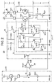
- Figure 2 is a circuit diagram of a first embodiment of a laser diode use drive circuit according to the present invention.
- This laser diode use drive circuit 20 is constituted by, as shown in Fig. 2, an input circuit 21, a differential output circuit 22, a reference voltage generation circuit 23, a comparison circuit 24, and a constant current setting use variable voltage supply circuit 25.
- the input circuit 21 is constituted by npn type transistors Q211 to Q214 and resistors R211 to R216, receives the differential drive signals D and DB, and supplies differential signals S21 and S21B in accordance with the level of the drive voltage VA supplied from the variable voltage supply circuit 25 to the differential output circuit 22.
- Emitters of the transistors Q211 and Q212 are connected to each other, and the connection point of these emitters is grounded via the resistor R211.
- the base of the transistor Q212 is connected to the input terminal TD of the drive signal D, and the collector is connected to the voltage supply line (emitter of the transistor Q252) of the variable voltage supply circuit 25 via the resistor R213.
- the base of the transistor Q211 is connected to the input terminal TDB of the drive signal DB taking a complementary level of the drive signal D, and the collector is connected to the voltage supply line of the variable voltage supply circuit 25 via the resistor R212.
- Emitters of the transistors Q213 and Q214 are connected to each other, and the connection point of these emitters is grounded via the resistor R214.
- the base of the transistor Q213 is connected to the collector of the transistor Q212, and the collector is connected to the voltage supply line of the variable voltage supply circuit 25 via the resistor R215.
- the base of the transistor Q214 is connected to the collector of the transistor Q211, and the collector is connected to the voltage supply line of the variable voltage supply circuit 25 via the resistor R216.
- the differential output circuit 22 is constituted by npn type transistors Q221 and Q222 and a resistor R221 having the resistance value R serving as the current/voltage conversion element. Receiving the differential signals S21 and S21B from the input circuit 21, the differential circuit switches and adjusts the amount of supply of the current to the laser diode LD to drives the same to emit light.
- Emitters of the transistors Q211 and Q222 are connected to each other, and the connection point of these emitters is grounded via the resistor R221.
- the base of the transistor Q221 is connected to the collector of the transistor Q213 of the input circuit 21, and the collector is connected to the (cathode of the) laser diode LD via a connection terminal T221.
- the base of the transistor Q222 is connected to the collector of the transistor Q214 of the input circuit 21, and the collector is connected to the supply line of the power supply voltage V CC via a connection terminal T222.
- One end of the resistor R231 is connected via a connection terminal T231 to the current source I231, and the connection point (node) N231 thereof is connected to one input of the comparison circuit 24.
- the other end of the resistor R231 is grounded.
- the comparison circuit 24 is constituted by an operational amplifier OP241, compares the voltage VD of the emitter-connection portion N221 of the differential output circuit 22 with the reference voltage VE generated at the reference voltage generation circuit 23, and outputs a signal S24 of a level in accordance with the result of comparison to the variable voltage supply circuit 25.
- the inverted input (-) of the operational amplifier OP241 is connected to the node N231 of the reference voltage generation circuit 23, and a non-inverted input (+) is connected to the emitter-connection portion N221 of the differential output circuit 22.
- the variable voltage supply circuit 25 is constituted by npn type transistors Q251 and Q252, a resistor R251, and a phase compensation use capacitor C251 and supplies a voltage VF in accordance with the input level of an output signal S24 of the comparison circuit 24 as the drive voltage VA of the input circuit 21.
- the supply voltage becomes a voltage (VF - Vf) down from the voltage VF by an amount of the forward direction bias Vf of the transistor Q252.
- the base of the transistor Q251 is connected to the output of the operational amplifier OP241 serving as the comparison circuit 24, the emitter is grounded, and the collector is connected to the base of the transistor Q252 and, at the same time, connected to the supply line of the power supply voltage V CC via the resistor R251 and connected to one electrode of the capacitor C251.
- the other electrode of the capacitor C251 is connected to the supply line of the power supply voltage V CC .
- the collector of the transistor Q252 is connected to the supply line of the power supply voltage V CC , and the emitter is connected to load use resistors R212, R213, R215, and R216 of the input circuit 21.
- the collector current of the transistor Q212 is increased, the transistor Q213 constituting the differential amplifier circuit of the latter stage becomes the OFF state, and an input signal receiving the amplification action is supplied to the base of the transistor Q221 of the differential output circuit 22 as the differential signal S21 of the level VB.
- the transistor Q214 constituting the differential amplifier circuit of the latter stage of the input circuit 21 is held in an ON state, and the differential signal S21B is supplied at a low level to the base of the transistor Q222 of the differential output circuit 22.
- the laser diode LD emits light.
- a modulation current such as substantially Iset x N flows in the resistor R221 connected to the emitter-connection portion side of the differential circuit. Accordingly, the potential VD of the emitter-connection portion N221 becomes substantially Iset x n x R This voltage VD is supplied (fed back) to the non-inverted input (+) of the operational amplifier OP241 serving as the comparison circuit 24.
- the comparison circuit 24 the voltage VD of the emitter-connection portion N221 of the differential output circuit 22 and the reference voltage VE generated at the reference voltage generation circuit 23 are compared, and a signal S24 of a level in accordance with the result of comparison is output to the variable voltage supply circuit 25. Specifically, when the voltage VD of the emitter-connection portion N221 is larger than the reference voltage VE, the level of the signal S24 is raised, while when it is smaller than the latter, the level of the signal S24 is lowered before output.
- variable voltage supply circuit 25 the amount of the current flowing in the transistor Q251 is adjusted in accordance with the level of the input signal S24, and a voltage VF determined by this variable current and the resistance value of the resistor R251 is generated.
- This voltage VF is supplied to the input circuit 21 as the drive voltage VA through the transistor Q252.
- the supply voltage becomes a voltage reduced from the voltage VF by an amount of the forward direction bias Vf of the transistor Q252 (VF - Vf).
- the levels of the differential signals S21 and S21B supplied from the input circuit 21 to the differential output circuit 22 are adjusted so that the level of the voltage VD of the emitter-connection portion N221 of the differential output circuit 22 becomes low when it is larger than the reference voltage VE, in other words, controlled so that the modulation current flowing in the differential output circuit 22 converges to n x Iset.
- the collector current of the transistor Q211 is increased, the transistor Q214 constituting the differential amplifier circuit of the latter stage becomes the OFF state, and an input signal receiving an amplification action is supplied to the base of the transistor Q222 of the differential output circuit 22 as the differential signal S21B of the level VB.
- the transistor Q213 constituting the differential amplifier circuit of the latter stage of the input circuit 21 is held in the ON state, and the differential signal S21 is supplied at a low level to the base of the transistor Q221 of the differential output circuit 22.
- the laser diode LD does not emit light.
- the laser diode LD is driven to emit light.
- the input circuit 21 which receives the differential drive signals D and DB and outputs the differential signals S21 and S21B of levels in accordance with the level of the drive voltage VA supplied from the variable voltage supply circuit 25; a differential output circuit 22 in which emitters of the transistors Q221 and Q222 are connected to each other, the emitter-connection portion N221 of them is grounded via the resistor R221 having a resistance value of R, the differential signals S21 and S21B are supplied to bases, and the laser diode LD is connected to the collector of the transistor Q221; the reference voltage generation circuit 23 which generates the reference voltage VE such as Iset x n x R; the comparison circuit 24 which compares the voltage VD of the emitter-connection portion N221 of the differential output circuit 22 and the reference voltage VE generated at the reference voltage generation circuit 23 and outputs the signal S24 of the level in accordance with the result of comparison; and the variable voltage supply circuit 25 which generates the voltage VF in accordance with
- the laser diode LD is driven by a differential circuit of transistors, so there is an advantage that a high speed and stable operation can be realized.
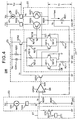
- Figure 3 is a circuit diagram of a second embodiment of a laser diode use drive circuit according to the present invention.
- the difference of the present second embodiment from the first embodiment resides in that, as the voltage to be compared with the reference voltage VE at the comparison circuit 24, in place of directly using the voltage VD of the emitter-connection portion N221 of the differential output circuit 22, provision is made of a dummy circuit 26 comprising an npn type transistor Q261 equivalent to the drive transistor Q221 of the differential output circuit 22 and a resistor R261 connected between the emitter of the transistor Q261 and the ground GND and in which the base of the transistor Q261 is connected to the voltage supply line of the variable voltage supply circuit 25 and the emitter-side voltage VG of the transistor Q261 is used as the comparison voltage.
- the size (emitter size) of the transistor Q261 in the dummy circuit 26 is set to 1/m of the transistors Q221 and Q222 of the differential circuit 22, and the resistance value of the resistor R261 is set to m x R, i.e., m times the resistance value R of the resistor R221.
- the size of the transistor can mean the area of the emitter, that is the junction area; the emitter current being proportional to the emitter area.
- the modulation current of the differential output circuit 22 is defined as IQ
- the current flowing in the dummy circuit 26 is controlled so that the current of 1/m of IQ flows and the voltage VG becomes (IQ/m) x m x R, that is, IQ x R
- This voltage IQ x R is equal to the voltage VD of the emitter-connection portion N221 of the differential output circuit 22.
- the collector current of the transistor Q212 is increased, the transistor Q213 constituting the differential amplifier circuit of the latter stage becomes the OFF state, and the input signal receiving the amplification action is supplied to the base of the transistor Q221 of the differential output circuit 22 as the differential signal S21 of the level VB.
- the transistor Q214 constituting the differential amplifier circuit of the latter stage of the input circuit 21 is held in the ON state, and the differential signal S21B is supplied at a low level to the base of the transistor Q222 of the differential output circuit 22.
- the laser diode LD emits light.
- the emitter side voltage VG of the dummy circuit 26 and the reference voltage VE generated at the reference voltage generation circuit 23 are compared, and a signal S24 of a level in accordance with the comparison result is output to the variable voltage supply circuit 25.
- the level of the signal S24 is raised, while when it is smaller than the latter, the level of the signal S24 is lowered before output.
- variable voltage supply circuit 25 the amount of the current flowing in the transistor Q251 is adjusted in accordance with the level of the input signal S24, and a voltage VF determined by this variable current and the resistance value of the resistor R251 is generated.
- this voltage VF is supplied to the input circuit 21 and the dummy circuit 26 as the drive voltage VA through the transistor Q252.
- the supply voltage becomes the voltage reduced from the voltage VF by an amount of the forward direction bias Vf of the transistor Q252 (VF - Vf).
- levels of the differential signals S21 and S21B supplied from the input circuit 21 to the differential output circuit 22 are adjusted so that the level of the emitter side voltage VG of the dummy circuit 26 equal to the voltage VD of the emitter-connection portion N221 of the differential output circuit 22 becomes low when it is larger than the reference voltage VE, in other words, controlled so that the modulation current flowing in the differential output circuit 22 converges to IQ(n x Iset).
- the adjustment is carried out so that the levels of the differential signals S21 and S21B supplied from the input circuit 21 to the differential output circuit 22 become high and similarly feedback control is carried out so that the modulation current flowing in the differential output circuit 22 converges to IQ(n x Iset).
- the collector current of the transistor Q211 is increased, the transistor Q214 constituting the differential amplifier circuit of the latter stage becomes the OFF state, and the input signal receiving the amplification action is supplied to the base of the transistor Q222 of the differential output circuit 22 as the differential signal S21B of the level VB.
- the transistor Q213 constituting the differential amplifier circuit of the latter stage of the input circuit 21 is held in the ON state, and the differential signal S21 is supplied to the base of the transistor Q221 of the differential output circuit 22 at a low level.
- the laser diode LD does not emit light.
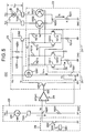
- Figure 4 is a circuit diagram of a third embodiment of a laser diode use drive circuit according to the present invention.
- the difference of the present third embodiment from the first embodiment resides in that provision is made of a shut down circuit 27 for making the emission of light (oscillation) of the laser diode LD forcibly stop in a case where for example the present drive circuit is applied to optical communications and an end face of an optical fiber serving as the path of propagation of the optical signal is arranged facing the face of a laser diode LD emitting the light (light firing) using a connector or the like, but the connection between the optical fiber and the light emitting (light firing) face of the laser diode LD becomes detached due to some reason or another or in a case of a safety circuit or the like for preventing an excess current from flowing in the laser diode LD, taking into consideration the effect on the human eye or damage to the laser diode LD.
- the shut down circuit 27 is constituted by a detection circuit 271 which detects an existence of abnormality of the state of connection of the optical fiber and the light emitting (light firing) face of the laser diode LD and outputs a detection signal S271 when detecting the abnormality and by a switch circuit 272 which connects the voltage output node N231 of the reference voltage generation circuit 23 to the ground line GND by making this bypass the resistor R231 when receiving the detection signal S271.
- the detection signal S271 is output to the switch circuit 272.
- the switch circuit 272 receiving the detection signal S271 becomes the ON state.
- the voltage output node N231 of the reference voltage generation circuit 23 is grounded, the voltage V D of the emitter-connection portion N221 of the differential output circuit 22 is grounded by feedback control, and the emission of light of the laser diode LD is forcibly stopped.
- Figure 5 is a circuit diagram of a fourth embodiment of the laser diode use drive circuit according to the present invention.
- the difference of the present fourth embodiment from the second embodiment is similar to the relationship between the third embodiment and the first embodiment.
- a shut down circuit 28 for making the emission of light (oscillation) of the laser diode LD forcibly stop in a case where for example the present drive circuit is applied to optical communications and an end face of an optical fiber serving as the path of propagation of the optical signal is arranged facing the face of a laser diode LD emitting the light (light firing) using a connector or the like, but the connection between the optical fiber and the light emitting (light firing) face of the laser diode LD becomes detached due to some reason or another or in a case of a safety circuit or the like for preventing an excess current from flowing in the laser diode LD, taking into consideration the effect on the human eye or damage to the laser diode LD.
- the shut down circuit 28 is constituted by a detection circuit 281 which detects an existence of an abnormality of the state of connection of the optical fiber and the light emitting (light firing) face of the laser diode LD and outputs a detection signal S281 when detecting the abnormality and by a switch circuit 282 which connects the voltage output node N231 of the reference voltage generation circuit 23 to the ground line GND by making this bypass the resistor R231 when receiving the detection signal S271.
- the detection signal S281 is output to the switch circuit 282.
- the switch circuit 282 receiving the detection signal S281 becomes the ON state.
- the voltage output node N231 of the reference voltage generation circuit 23 is grounded, the supply of the drive voltage to the input circuit 21 is stopped, and the emission of light of the laser diode LD is forcibly stopped.
- the transistor for the constant current source of the current mirror circuit becomes unnecessary, saturation does not occur even when a large modulation current is set, and the desired constant current (modulation current) can be set while holding the forward direction voltage required by the light emitting element even under a low power supply voltage.
- the light emitting element is driven by a differential circuit of transistors, a stable, high speed operation can be realized.
- a current setting ratio further stabler and higher in precision with respect to variations of the process, temperature changes, and fluctuations in the power supply can be secured.
- shut down circuit since a shut down circuit is provided, there is an advantage that the light emission can be controlled more stably.
Applications Claiming Priority (2)
| Application Number | Priority Date | Filing Date | Title |
|---|---|---|---|
| JP04767098A JP4200535B2 (ja) | 1998-02-27 | 1998-02-27 | 発光素子の駆動回路 |
| JP4767098 | 1998-02-27 |
Publications (3)
| Publication Number | Publication Date |
|---|---|
| EP0939468A2 true EP0939468A2 (fr) | 1999-09-01 |
| EP0939468A3 EP0939468A3 (fr) | 2004-01-28 |
| EP0939468B1 EP0939468B1 (fr) | 2006-12-20 |
Family
ID=12781710
Family Applications (1)
| Application Number | Title | Priority Date | Filing Date |
|---|---|---|---|
| EP99301474A Expired - Lifetime EP0939468B1 (fr) | 1998-02-27 | 1999-02-26 | Circuit de commande d'un élément émetteur de lumière |
Country Status (4)
| Country | Link |
|---|---|
| US (1) | US6097159A (fr) |
| EP (1) | EP0939468B1 (fr) |
| JP (1) | JP4200535B2 (fr) |
| DE (1) | DE69934448T2 (fr) |
Cited By (1)
| Publication number | Priority date | Publication date | Assignee | Title |
|---|---|---|---|---|
| CN106129805A (zh) * | 2016-05-25 | 2016-11-16 | 无锡亮源激光技术有限公司 | 一种半导体激光照射源电路 |
Families Citing this family (57)
| Publication number | Priority date | Publication date | Assignee | Title |
|---|---|---|---|---|
| US6111643A (en) * | 1997-10-28 | 2000-08-29 | Reliance Electric Industrial Company | Apparatus, system and method for determining wear of an article |
| JP4581154B2 (ja) * | 1999-02-18 | 2010-11-17 | ソニー株式会社 | 半導体レーザ駆動回路および光ディスク装置 |
| JP3507738B2 (ja) * | 1999-11-30 | 2004-03-15 | 松下電器産業株式会社 | レーザ駆動装置 |
| JP2001251011A (ja) * | 2000-03-06 | 2001-09-14 | Oki Electric Ind Co Ltd | レーザダイオード駆動回路 |
| US6728494B2 (en) * | 2000-06-08 | 2004-04-27 | Matsushita Electric Industrial Co., Ltd. | Light-emitting device drive circuit, and optical transmission system using the circuit |
| US7606492B2 (en) | 2000-10-04 | 2009-10-20 | Enablence Usa Fttx Networks Inc. | System and method for communicating optical signals upstream and downstream between a data service provider and subscribers |
| US7130541B2 (en) * | 2000-10-04 | 2006-10-31 | Wave7 Optics, Inc. | System and method for communicating optical signals upstream and downstream between a data service provider and subscriber |
| US6973271B2 (en) | 2000-10-04 | 2005-12-06 | Wave7 Optics, Inc. | System and method for communicating optical signals between a data service provider and subscribers |
| CA2426831A1 (fr) * | 2000-10-26 | 2002-08-01 | Wave7 Optics, Inc. | Procede et systeme de traitement en aval de paquets d'un reseau optique |
| CN100428592C (zh) * | 2001-03-05 | 2008-10-22 | 富士施乐株式会社 | 发光元件驱动装置和发光元件驱动系统 |
| JP4123791B2 (ja) * | 2001-03-05 | 2008-07-23 | 富士ゼロックス株式会社 | 発光素子駆動装置および発光素子駆動システム |
| EP1261082A1 (fr) * | 2001-05-25 | 2002-11-27 | Agilent Technologies, Inc. (a Delaware corporation) | Circuit optoélectronique et circuit de commande |
| WO2003005612A1 (fr) | 2001-07-05 | 2003-01-16 | Wave7 Optics, Inc. | Procedes et systemes offrant un trajet de retour a des signaux generes par des terminaux classiques dans un reseau optique |
| US7218855B2 (en) * | 2001-07-05 | 2007-05-15 | Wave7 Optics, Inc. | System and method for communicating optical signals to multiple subscribers having various bandwidth demands connected to the same optical waveguide |
| US7190901B2 (en) * | 2001-07-05 | 2007-03-13 | Wave7 Optices, Inc. | Method and system for providing a return path for signals generated by legacy terminals in an optical network |
| US7529485B2 (en) * | 2001-07-05 | 2009-05-05 | Enablence Usa Fttx Networks, Inc. | Method and system for supporting multiple services with a subscriber optical interface located outside a subscriber's premises |
| US7146104B2 (en) | 2001-07-05 | 2006-12-05 | Wave7 Optics, Inc. | Method and system for providing a return data path for legacy terminals by using existing electrical waveguides of a structure |
| US7269350B2 (en) * | 2001-07-05 | 2007-09-11 | Wave7 Optics, Inc. | System and method for communicating optical signals between a data service provider and subscribers |
| US7333726B2 (en) * | 2001-07-05 | 2008-02-19 | Wave7 Optics, Inc. | Method and system for supporting multiple service providers within a single optical network |
| US7877014B2 (en) | 2001-07-05 | 2011-01-25 | Enablence Technologies Inc. | Method and system for providing a return path for signals generated by legacy video service terminals in an optical network |
| US6654565B2 (en) * | 2001-07-05 | 2003-11-25 | Wave7 Optics, Inc. | System and method for increasing upstream communication efficiency in an optical network |
| US7593639B2 (en) | 2001-08-03 | 2009-09-22 | Enablence Usa Fttx Networks Inc. | Method and system for providing a return path for signals generated by legacy terminals in an optical network |
| WO2003021820A1 (fr) * | 2001-08-28 | 2003-03-13 | Wave7 Optics, Inc. | Systeme et procede permettant d'ameliorer l'efficacite des communications vers l'amont dans un reseau de transmission optique |
| US7038910B1 (en) | 2002-01-07 | 2006-05-02 | Wave7 Optics, Inc. | System and method for removing heat from a subscriber optical interface |
| US7583897B2 (en) | 2002-01-08 | 2009-09-01 | Enablence Usa Fttx Networks Inc. | Optical network system and method for supporting upstream signals propagated according to a cable modem protocol |
| US20030174747A1 (en) * | 2002-03-18 | 2003-09-18 | Wyman Theodore J. | Low voltage laser driver |
| TW529186B (en) * | 2002-04-12 | 2003-04-21 | Ind Tech Res Inst | Light-emitting device driving circuit |
| US7623786B2 (en) | 2002-05-20 | 2009-11-24 | Enablence Usa Fttx Networks, Inc. | System and method for communicating optical signals to multiple subscribers having various bandwidth demands connected to the same optical waveguide |
| US6707257B2 (en) * | 2002-08-08 | 2004-03-16 | Datex-Ohmeda, Inc. | Ferrite stabilized LED drive |
| US6720734B2 (en) * | 2002-08-08 | 2004-04-13 | Datex-Ohmeda, Inc. | Oximeter with nulled op-amp current feedback |
| US6825619B2 (en) * | 2002-08-08 | 2004-11-30 | Datex-Ohmeda, Inc. | Feedback-controlled LED switching |
| US7058260B2 (en) * | 2002-10-15 | 2006-06-06 | Wave7 Optics, Inc. | Reflection suppression for an optical fiber |
| US7454141B2 (en) | 2003-03-14 | 2008-11-18 | Enablence Usa Fttx Networks Inc. | Method and system for providing a return path for signals generated by legacy terminals in an optical network |
| US6879608B1 (en) * | 2003-03-31 | 2005-04-12 | Applied Micro Circuits Corporation | High compliance laser driver |
| WO2006020538A2 (fr) * | 2004-08-10 | 2006-02-23 | Wave7 Optics, Inc. | Contre-mesures pour interference entre des modeles au repos affectes par une diffusion raman stimulee dans des systemes de reseau optique ethernet |
| US7599622B2 (en) | 2004-08-19 | 2009-10-06 | Enablence Usa Fttx Networks Inc. | System and method for communicating optical signals between a data service provider and subscribers |
| KR101061847B1 (ko) | 2004-08-20 | 2011-09-02 | 삼성전자주식회사 | 전원 공급 장치 및 백라이트 장치 |
| US7630422B1 (en) * | 2005-01-14 | 2009-12-08 | National Semiconductor Corporation | Driver for vertical-cavity surface-emitting laser and method |
| US7616901B2 (en) | 2005-08-10 | 2009-11-10 | Enablence Usa Fttx Networks Inc. | Countermeasures for idle pattern SRS interference in ethernet optical network systems |
| US8362436B1 (en) | 2006-03-14 | 2013-01-29 | Advanced Precision Inc. | Electro-optic fluid quantity measurement system |
| JP2008016732A (ja) * | 2006-07-07 | 2008-01-24 | Mitsumi Electric Co Ltd | 発光ダイオード駆動回路 |
| TWI326563B (en) * | 2006-10-18 | 2010-06-21 | Chunghwa Picture Tubes Ltd | Light source driving circuit |
| US7671539B1 (en) | 2006-11-16 | 2010-03-02 | Advanced Precision Inc. | Systems and methods for generating optical energy using a light-emitting diode |
| JPWO2009011019A1 (ja) * | 2007-07-13 | 2010-09-09 | 三菱電機株式会社 | 光送信器 |
| JP5035054B2 (ja) * | 2008-03-19 | 2012-09-26 | 住友電気工業株式会社 | 半導体レーザ駆動回路 |
| US7756173B2 (en) * | 2008-06-20 | 2010-07-13 | Alfrey Anthony J | Laser diode driver with adaptive compliance voltage |
| US8948607B2 (en) * | 2008-10-09 | 2015-02-03 | Finisar Corporation | Active linear amplifier inside transmitter module |
| JP2010246287A (ja) * | 2009-04-07 | 2010-10-28 | Renesas Electronics Corp | 電流制御回路 |
| JP5509662B2 (ja) * | 2009-04-13 | 2014-06-04 | ソニー株式会社 | レーザ駆動装置 |
| DE102009018701B4 (de) * | 2009-04-23 | 2011-03-24 | Texas Instruments Deutschland Gmbh | Elektronische Vorrichtung und Verfahren zur Ansteuerung einer licht-emittierenden Halbleitervorrichtung |
| JP5803174B2 (ja) * | 2010-09-09 | 2015-11-04 | 富士通株式会社 | 駆動回路 |
| WO2013162535A1 (fr) * | 2012-04-25 | 2013-10-31 | Hewlett-Packard Development Company, L.P. | Fonctionnement de lasers à cavité verticale émettant par la surface |
| US9025629B2 (en) * | 2012-12-03 | 2015-05-05 | Micrel, Inc. | High compliance laser driver circuit |
| JP6601372B2 (ja) * | 2016-11-25 | 2019-11-06 | 株式会社デンソー | ゲート駆動装置 |
| US11239632B2 (en) * | 2019-06-02 | 2022-02-01 | Artilux, Inc. | Laser driving apparatus with current control circuitry and multi-channel circuitry |
| JP2021077970A (ja) | 2019-11-07 | 2021-05-20 | 住友電気工業株式会社 | 駆動回路 |
| CN114498290B (zh) * | 2022-04-14 | 2022-07-12 | 武汉博激世纪科技有限公司 | 一种半导体激光治疗仪控制系统及方法 |
Citations (2)
| Publication number | Priority date | Publication date | Assignee | Title |
|---|---|---|---|---|
| US5123023A (en) * | 1990-11-21 | 1992-06-16 | Polaroid Corporation | Laser driver with plural feedback loops |
| EP0756362A1 (fr) * | 1995-07-28 | 1997-01-29 | Nec Corporation | Circuit de commande de diode laser commandé en tension |
Family Cites Families (3)
| Publication number | Priority date | Publication date | Assignee | Title |
|---|---|---|---|---|
| GB2024438B (en) * | 1978-06-30 | 1983-04-27 | Canon Kk | Electrophotographic copier |
| US4998043A (en) * | 1989-05-01 | 1991-03-05 | Fujikura Ltd. | LED stabilizing light source device |
| US5638390A (en) * | 1995-07-27 | 1997-06-10 | Methode Electronics, Inc. | Optoelectronic transceiver module laser diode stabilizer and bias control method |
-
1998
- 1998-02-27 JP JP04767098A patent/JP4200535B2/ja not_active Expired - Fee Related
-
1999
- 1999-02-24 US US09/256,094 patent/US6097159A/en not_active Expired - Fee Related
- 1999-02-26 EP EP99301474A patent/EP0939468B1/fr not_active Expired - Lifetime
- 1999-02-26 DE DE69934448T patent/DE69934448T2/de not_active Expired - Fee Related
Patent Citations (2)
| Publication number | Priority date | Publication date | Assignee | Title |
|---|---|---|---|---|
| US5123023A (en) * | 1990-11-21 | 1992-06-16 | Polaroid Corporation | Laser driver with plural feedback loops |
| EP0756362A1 (fr) * | 1995-07-28 | 1997-01-29 | Nec Corporation | Circuit de commande de diode laser commandé en tension |
Cited By (2)
| Publication number | Priority date | Publication date | Assignee | Title |
|---|---|---|---|---|
| CN106129805A (zh) * | 2016-05-25 | 2016-11-16 | 无锡亮源激光技术有限公司 | 一种半导体激光照射源电路 |
| CN106129805B (zh) * | 2016-05-25 | 2021-11-26 | 无锡亮源激光技术有限公司 | 一种半导体激光照射源电路 |
Also Published As
| Publication number | Publication date |
|---|---|
| EP0939468B1 (fr) | 2006-12-20 |
| US6097159A (en) | 2000-08-01 |
| EP0939468A3 (fr) | 2004-01-28 |
| DE69934448D1 (de) | 2007-02-01 |
| JP4200535B2 (ja) | 2008-12-24 |
| DE69934448T2 (de) | 2007-09-27 |
| JPH11251668A (ja) | 1999-09-17 |
Similar Documents
| Publication | Publication Date | Title |
|---|---|---|
| US6097159A (en) | Drive circuit of light emitting element | |
| JP2704133B2 (ja) | レーザダイオード駆動回路 | |
| US8023541B2 (en) | Optical transmission circuit | |
| KR101072169B1 (ko) | Led 구동 회로 | |
| JPH0529688A (ja) | 半導体レーザアレイ装置 | |
| JPH07240554A (ja) | 半導体レーザ駆動装置 | |
| US6229833B1 (en) | Laser diode protecting circuit and laser driving current control circuit | |
| JP2001352125A (ja) | Apc方式レーザダイオード駆動回路 | |
| CN1989627A (zh) | Led驱动电路 | |
| JPH10261827A (ja) | レーザーダイオードの駆動回路および駆動方法 | |
| US6535534B1 (en) | Optical source driver with bias circuit for controlling output overshoot | |
| JP3423115B2 (ja) | 光信号送信装置 | |
| JPH07321392A (ja) | レーザダイオードの自動温度制御回路及びこれを用いた電気/光信号変換ユニット | |
| US7856039B2 (en) | Semiconductor device and semiconductor laser driving device | |
| US5397933A (en) | Laser diode driving circuit having a temperature compensation circuit | |
| US7141936B2 (en) | Driving circuit for light emitting diode | |
| US6072816A (en) | Laser-diode drive circuit | |
| JPH10270784A (ja) | Ld駆動回路 | |
| JP2006100555A (ja) | 発光素子駆動回路および前置増幅回路 | |
| JP2791004B2 (ja) | レーザダイオード駆動回路 | |
| Lupo et al. | Study of DAC architectures for integrated laser driver systems | |
| JPS63110685A (ja) | 発光素子の駆動回路 | |
| JP2000261090A (ja) | レーザ駆動回路 | |
| JPH0595148A (ja) | レーザダイオード駆動回路 | |
| JPS627183A (ja) | 半導体レ−ザの光出力安定化回路 |
Legal Events
| Date | Code | Title | Description |
|---|---|---|---|
| PUAI | Public reference made under article 153(3) epc to a published international application that has entered the european phase |
Free format text: ORIGINAL CODE: 0009012 |
|
| AK | Designated contracting states |
Kind code of ref document: A2 Designated state(s): AT BE CH CY DE DK ES FI FR GB GR IE IT LI LU MC NL PT SE |
|
| AX | Request for extension of the european patent |
Free format text: AL;LT;LV;MK;RO;SI |
|
| PUAL | Search report despatched |
Free format text: ORIGINAL CODE: 0009013 |
|
| AK | Designated contracting states |
Kind code of ref document: A3 Designated state(s): AT BE CH CY DE DK ES FI FR GB GR IE IT LI LU MC NL PT SE |
|
| AX | Request for extension of the european patent |
Extension state: AL LT LV MK RO SI |
|
| RIC1 | Information provided on ipc code assigned before grant |
Ipc: 7H 01S 5/042 B Ipc: 7H 01S 5/068 B Ipc: 7H 01S 3/096 A |
|
| 17P | Request for examination filed |
Effective date: 20040629 |
|
| AKX | Designation fees paid |
Designated state(s): DE GB |
|
| 17Q | First examination report despatched |
Effective date: 20050506 |
|
| GRAP | Despatch of communication of intention to grant a patent |
Free format text: ORIGINAL CODE: EPIDOSNIGR1 |
|
| GRAC | Information related to communication of intention to grant a patent modified |
Free format text: ORIGINAL CODE: EPIDOSCIGR1 |
|
| RIC1 | Information provided on ipc code assigned before grant |
Ipc: H01S 5/042 20060101ALI20060712BHEP Ipc: H01S 5/068 20060101AFI20060712BHEP |
|
| GRAS | Grant fee paid |
Free format text: ORIGINAL CODE: EPIDOSNIGR3 |
|
| GRAA | (expected) grant |
Free format text: ORIGINAL CODE: 0009210 |
|
| AK | Designated contracting states |
Kind code of ref document: B1 Designated state(s): DE GB |
|
| REG | Reference to a national code |
Ref country code: GB Ref legal event code: FG4D |
|
| REF | Corresponds to: |
Ref document number: 69934448 Country of ref document: DE Date of ref document: 20070201 Kind code of ref document: P |
|
| PLBE | No opposition filed within time limit |
Free format text: ORIGINAL CODE: 0009261 |
|
| STAA | Information on the status of an ep patent application or granted ep patent |
Free format text: STATUS: NO OPPOSITION FILED WITHIN TIME LIMIT |
|
| 26N | No opposition filed |
Effective date: 20070921 |
|
| PGFP | Annual fee paid to national office [announced via postgrant information from national office to epo] |
Ref country code: DE Payment date: 20090219 Year of fee payment: 11 |
|
| PGFP | Annual fee paid to national office [announced via postgrant information from national office to epo] |
Ref country code: GB Payment date: 20090225 Year of fee payment: 11 |
|
| GBPC | Gb: european patent ceased through non-payment of renewal fee |
Effective date: 20100226 |
|
| PG25 | Lapsed in a contracting state [announced via postgrant information from national office to epo] |
Ref country code: DE Free format text: LAPSE BECAUSE OF NON-PAYMENT OF DUE FEES Effective date: 20100901 |
|
| PG25 | Lapsed in a contracting state [announced via postgrant information from national office to epo] |
Ref country code: GB Free format text: LAPSE BECAUSE OF NON-PAYMENT OF DUE FEES Effective date: 20100226 |