EP0932085A1 - Dispositif et procede de formation d'image - Google Patents
Dispositif et procede de formation d'image Download PDFInfo
- Publication number
- EP0932085A1 EP0932085A1 EP97942248A EP97942248A EP0932085A1 EP 0932085 A1 EP0932085 A1 EP 0932085A1 EP 97942248 A EP97942248 A EP 97942248A EP 97942248 A EP97942248 A EP 97942248A EP 0932085 A1 EP0932085 A1 EP 0932085A1
- Authority
- EP
- European Patent Office
- Prior art keywords
- photosensitive member
- exposure
- image
- light beam
- gray
- Prior art date
- Legal status (The legal status is an assumption and is not a legal conclusion. Google has not performed a legal analysis and makes no representation as to the accuracy of the status listed.)
- Granted
Links
- 238000000034 method Methods 0.000 title claims abstract description 76
- 230000035945 sensitivity Effects 0.000 claims abstract description 47
- 238000009826 distribution Methods 0.000 claims abstract description 42
- 238000012546 transfer Methods 0.000 claims description 18
- 238000011161 development Methods 0.000 claims description 16
- 229910021417 amorphous silicon Inorganic materials 0.000 claims description 4
- 239000003086 colorant Substances 0.000 claims description 4
- 239000000126 substance Substances 0.000 claims description 3
- 230000015572 biosynthetic process Effects 0.000 abstract description 40
- 238000009792 diffusion process Methods 0.000 abstract description 13
- 238000013016 damping Methods 0.000 abstract description 12
- 230000005684 electric field Effects 0.000 abstract description 10
- 238000012545 processing Methods 0.000 description 12
- 239000002245 particle Substances 0.000 description 6
- 238000004140 cleaning Methods 0.000 description 5
- 230000002411 adverse Effects 0.000 description 4
- 230000002035 prolonged effect Effects 0.000 description 4
- 239000007787 solid Substances 0.000 description 4
- 230000001678 irradiating effect Effects 0.000 description 3
- 206010034972 Photosensitivity reaction Diseases 0.000 description 2
- XUIMIQQOPSSXEZ-UHFFFAOYSA-N Silicon Chemical compound [Si] XUIMIQQOPSSXEZ-UHFFFAOYSA-N 0.000 description 2
- 239000000969 carrier Substances 0.000 description 2
- 230000006866 deterioration Effects 0.000 description 2
- 238000005516 engineering process Methods 0.000 description 2
- 239000000203 mixture Substances 0.000 description 2
- 238000012986 modification Methods 0.000 description 2
- 230000004048 modification Effects 0.000 description 2
- 230000002093 peripheral effect Effects 0.000 description 2
- 230000036211 photosensitivity Effects 0.000 description 2
- 238000007639 printing Methods 0.000 description 2
- 229910052710 silicon Inorganic materials 0.000 description 2
- 239000010703 silicon Substances 0.000 description 2
- 230000000087 stabilizing effect Effects 0.000 description 2
- 229910000859 α-Fe Inorganic materials 0.000 description 2
- 238000005299 abrasion Methods 0.000 description 1
- 238000004891 communication Methods 0.000 description 1
- 238000007796 conventional method Methods 0.000 description 1
- 238000007599 discharging Methods 0.000 description 1
- 238000010438 heat treatment Methods 0.000 description 1
- 238000001454 recorded image Methods 0.000 description 1
- 230000004044 response Effects 0.000 description 1
- 238000007790 scraping Methods 0.000 description 1
- 238000012216 screening Methods 0.000 description 1
- 238000011144 upstream manufacturing Methods 0.000 description 1
Images
Classifications
-
- G—PHYSICS
- G03—PHOTOGRAPHY; CINEMATOGRAPHY; ANALOGOUS TECHNIQUES USING WAVES OTHER THAN OPTICAL WAVES; ELECTROGRAPHY; HOLOGRAPHY
- G03G—ELECTROGRAPHY; ELECTROPHOTOGRAPHY; MAGNETOGRAPHY
- G03G15/00—Apparatus for electrographic processes using a charge pattern
- G03G15/22—Apparatus for electrographic processes using a charge pattern involving the combination of more than one step according to groups G03G13/02 - G03G13/20
- G03G15/32—Apparatus for electrographic processes using a charge pattern involving the combination of more than one step according to groups G03G13/02 - G03G13/20 in which the charge pattern is formed dotwise, e.g. by a thermal head
- G03G15/326—Apparatus for electrographic processes using a charge pattern involving the combination of more than one step according to groups G03G13/02 - G03G13/20 in which the charge pattern is formed dotwise, e.g. by a thermal head by application of light, e.g. using a LED array
-
- G—PHYSICS
- G03—PHOTOGRAPHY; CINEMATOGRAPHY; ANALOGOUS TECHNIQUES USING WAVES OTHER THAN OPTICAL WAVES; ELECTROGRAPHY; HOLOGRAPHY
- G03G—ELECTROGRAPHY; ELECTROPHOTOGRAPHY; MAGNETOGRAPHY
- G03G15/00—Apparatus for electrographic processes using a charge pattern
- G03G15/04—Apparatus for electrographic processes using a charge pattern for exposing, i.e. imagewise exposure by optically projecting the original image on a photoconductive recording material
- G03G15/04036—Details of illuminating systems, e.g. lamps, reflectors
- G03G15/04045—Details of illuminating systems, e.g. lamps, reflectors for exposing image information provided otherwise than by directly projecting the original image onto the photoconductive recording material, e.g. digital copiers
-
- H—ELECTRICITY
- H04—ELECTRIC COMMUNICATION TECHNIQUE
- H04N—PICTORIAL COMMUNICATION, e.g. TELEVISION
- H04N1/00—Scanning, transmission or reproduction of documents or the like, e.g. facsimile transmission; Details thereof
- H04N1/23—Reproducing arrangements
- H04N1/29—Reproducing arrangements involving production of an electrostatic intermediate picture
- H04N1/295—Circuits or arrangements for the control thereof, e.g. using a programmed control device, according to a measured quantity
Definitions
- the present invention relates to an image forming apparatus and an image forming method suitable for forming color images by a gray-level image forming technique.
- Japanese Patent Application Laid-Open No. 1-297269 discloses a method in which the amount of light for black information recording by a light emitting device which forms an electrostatic latent image on a photosensitive member is set within the saturation range of the damping characteristics of the photosensitive member. Within the saturation range, the potential of the photosensitive member does not fluctuate greatly along with a fluctuation of the amount of light of the light emitting device. Thus, density unevenness due to a fluctuation of the amount of light emitted from the light emitting device can be prevented.
- Japanese Patent Application Laid-Open NO. 4-25871 discloses a technique in which a high ⁇ -photosensitive member is employed, and the relationship between the maximum light amount I 0 of the beam amount distribution on the high ⁇ -photosensitive member and the half exposure light amount P 1/2 for reducing the potential of the photosensitive member by half is defined as: 1.2 ⁇ P 1/2 ⁇ I 0 ⁇ 2.5 ⁇ P 1/2 .
- Japanese Patent Application Laid-Open No. 8-160677 also discloses an image forming process called a simultaneous cleaning method or a cleanerless method, in which the exposure intensity in the exposure process is set in a predetermined range so that excellent image formation can be obtained, though residual toners on the photosensitive member are again charged and exposed. In this manner, ghost images can be prevented, and high-resolution and excellent gray-level images can be obtained.
- a half-tone technique which uses “saturation write”
- banding which is caused by small fluctuations of the write position in the sub-scan direction.
- the image formation using an electrophotographic technique is essentially an analog system, in which each dot can be easily multi-valued.
- a write unit a laser diode, for instance
- fine image formation can be carried out with each pixel having a gray-level. If a dot area modulation method, such as a dither method and an error diffusion method, is employed without multi-valuing each dot, obtained color images cannot be considered for practical use.
- HIEST As a technique for improving gray-level reproducibility, there is a method called HIEST, in which the number of lines in a specific direction depending on the gray level (disclosed in "New Halftone Screening Technology Focused on Highlight Image Reproduction", Japan Hardcopy, 1995).
- the pulse-width modulation method and the HIEST method are designed to improve stability against various fluctuations caused by multi-valuing in the electrophotographic process.
- the "saturation write” is performed to apply a large enough amount of light to the photosensitive member, those methods are not effective in carrying out high-precision and stable image formation.
- An object of the present invention is to provide an image forming apparatus and an image forming method for carrying out high-precision and stable image formation.
- the apparatus and method of the present invention when a sufficient amount of light for carrying out "saturation write" is emitted onto the photosensitive member, the relationship between the exposure diameter and the thickness of the photosensitive layer, and the relationship between the maximum exposure and the differential sensitivity of the photosensitive member, are defined so as to restrict the charge diffusion and the electric field on the photosensitive layer.
- the image forming apparatus of the present invention comprises: a photosensitive member having a photosensitive layer (thickness: Tp) on its surface; a charging unit for uniformly charging the surface of the photosensitive member; an image exposure unit for exposing the uniformly charged photosensitive member with a light beam so as to form an electrostatic latent image; a gray-level image device for transmitting a drive signal to the image exposure unit and presenting a gray-level image in accordance with a gray-level signal based on image data including gray-level information; a developing unit for developing an electrostatic latent image formed on the photosensitive member; and a transferring unit for transferring a developed image from the photosensitive member onto a recording medium.
- a photosensitive member having a photosensitive layer (thickness: Tp) on its surface
- a charging unit for uniformly charging the surface of the photosensitive member
- an image exposure unit for exposing the uniformly charged photosensitive member with a light beam so as to form an electrostatic latent image
- a gray-level image device for
- the relationship between the layer thickness Tp and the exposure diameter Db is defined as 2Tp ⁇ Db, where the exposure diameter Db of the light beam is the minimum diameter at 1/e 2 with respect to the peak value of the exposure distribution determined by integrating the energy distribution of the light beam on the photosensitive member with the exposure time.
- the maximum exposure within the exposure diameter Db is set at a value that makes the differential sensitivity of the photosensitive layer small enough. More specifically, the maximum exposure within the exposure diameter Db is set at a value that reduces the differential sensitivity of the photosensitive layer to less than a third of its maximum value.
- the “energy distribution of the light beam” indicates the energy distribution of the light beam emitted from the image exposure unit.
- the exposure time integrated with respect to the energy distribution of the light beam is the time of scanning in the main-scan direction.
- the exposure time integrated with respect to the energy distribution of the light beam is the time of scanning in the sub-scan direction during the rotation of the photosensitive member.
- the "differential sensitivity" is defined with the relationship between the surface potential V(E) of the photosensitive member and the exposure E when the photosensitive member is uniformly exposed with a light beam having the same wavelength as the light beam emitted from the image exposure unit.
- the differential sensitivity is defined as:
- E is the amount of exposure light
- dE is a small value added to the Exposure E
- V(E + dE) is the surface potential of the photosensitive member.
- the differential sensitivity reduces as the exposure E increases.
- the "value that makes the differential sensitivity small enough” is the value of exposure that can utilize the range of the damping characteristics of the photosensitive member to obtain stability as well as excellent gray-level image presentation by the gray-level image device.
- the "stability to be obtained” is to prevent "banding”.
- the "value that makes the differential sensitivity small enough” is a value that reduces the differential sensitivity of the photosensitive layer to less than a third of its maximum value.
- the image exposure unit exposes the uniformly charged photosensitive member with a light beam so as to form an electrostatic latent image.
- the maximum exposure within the exposure diameter Db is set at the value that makes the differential sensitivity of the photosensitive layer small enough, or at the value that reduces the differential sensitivity of the photosensitive layer to less than a third of its maximum value.
- the layer thickness Tp of the photosensitive layer and the exposure diameter Db is defined as 2Tp ⁇ Db, the charge diffusion and the electric field expansion on the photosensitive layer are restricted. This prevents adverse influence from various mechanical fluctuations, and a blur in an electrostatic latent image.
- the diameter of the light beam spot is made small so as to obtain good gray-level image presentation, and the relationship between the layer thickness Tp of the photosensitive layer and the exposure diameter Db is set so as to prevent pixel expansion on the photosensitive layer of the photosensitive member.
- the intensity of the light beam is set so that high-quality image formation can be carried out regardless of various mechanical fluctuations.
- high-precision and stable image formation can be carried out, while maintaining excellent gray-level image presentation.
- the maximum exposure within the exposure diameter Db which is the value that makes the differential sensitivity of the photosensitive layer small enough or that reduces the differential sensitivity of the photosensitive layer to less than a third of its maximum value, can be in a range in which the photosensitive member has not reached the saturation range.
- the gray-level image device can presents gray-level images by not only a dot area modulation method but also a dot density modulation method.
- the relationship between the layer thickness Tp of the photosensitive layer and the exposure diameter Db is defined as 2Tp ⁇ Db
- charge diffusion and electric field expansion on the photosensitive layer can be restricted so as to obtain fine dots. In this manner, precise gray-level image representation can be achieved by the dot area modulation method.
- the "value that makes the differential sensitivity small enough" i.e., the “the value of exposure that can utilize the range of the damping characteristics of the photosensitive member to obtain stability as well as excellent gray-level image presentation by the gray-level image device"
- the “value that makes the differential sensitivity small enough” i.e., the “the value of exposure that can utilize the range of the damping characteristics of the photosensitive member to obtain stability as well as excellent gray-level image presentation by the gray-level image device”
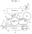
- Fig. 1 is a schematic view of an image forming apparatus.
- the image forming apparatus comprises a sheet feeding unit 2 containing transfer sheets 1 as a recording medium, a sheet transporting path 3 communicating with a sheet discharging unit (not shown), and an image processing unit 5 including a fixing unit 4 in the sheet transporting path 3.
- the image processing unit 5 is formed around a photosensitive member 6 in the form of a photosensitive drum.
- the photosensitive member 6 is surrounded by a charging unit 7, a developing unit 8, a transferring unit 9, and a cleaning unit 10, in that order.
- An exposure point EX is situated between the charging unit 7 and the developing unit 8, and the image processing unit 5 is provided with an image exposure unit 11 for irradiating the exposure point EX with a light beam that is a laser beam.
- the charging unit 7 applies electric charges to the photosensitive member 6 by corona electric charging, so that the photosensitive member 6 is uniformly charged with one polarity.
- the image exposure unit 11 irradiates the exposure point EX with a light beam in accordance with image information, so as to form an electrostatic latent image on the photosensitive member 6.
- a potential difference occurs in the irradiated area on the photosensitive member 6, and the irradiated area forms the electrostatic latent image.
- the developing unit 8 applies toners of the reverse polarity to the electrostatic latent image formed at the exposure point EX on the photosensitive member 6, thereby developing an image.
- the transferring unit 9 picks up the toner image developed on the photosensitive member 6 with the electric potential of reverse polarity, and then transfers the toner image onto a transfer sheet 1.
- the sheet transporting path 3 has a transporting structure for transporting the transfer sheet 1.
- the cleaning unit 10 cleans the photosensitive member 6 by scraping residual toners off the photosensitive member 6 after the transferring process.
- the fixing unit 4 is disposed on the downstream side of the transferring unit 9 in the sheet transporting path 3, and fixes the non-fixed toners adhering to the transfer sheet 1 by heating and pressurizing them after the transfer sheet 1 has passed through the transferring unit 9.
- the image forming apparatus of this embodiment further comprises a system control unit 12 having a structure of a microcomputer for controlling the other units.
- the system control unit 12 consists of a CPU for controlling the other units by executing various operations, a ROM for storing fixed data, and a RAM for storing variable data and used as a work area (none of them is shown in the figure).
- the system control unit 12 is connected to an image memory, for instance, which develops and holds the drive control circuit and image information of each of the other units (none of them is shown in the figure).
- the system control unit 12 controls the drive of each unit, thereby forming an image by an electrophotographic process.
- the image exposure unit 11 is controlled by an image signal and a control signal outputted from the system control unit 12, so that it irradiates the exposure point EX on the photosensitive member 6 with a light beam in accordance with the image information.
- the image forming apparatus of this embodiment is provided with a gray-level image device to be operated by the microcomputer of the system control unit 12.
- the gray-level image device controls the drive of the image exposure unit 11 based on image data including gray-level information. More specifically, the gray-level image device is operated by a known gray-level image presenting method such as an error diffusion method and a dither method.
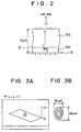
- Fig. 2 is a sectional view of a photosensitive layer 12 of the photosensitive member 6.
- the photosensitive member 6 is an organic photosensitive member.
- the photosensitive layer 12 of the photosensitive member 6 is made up of a charge generation layer 12a disposed on the base side of the photosensitive member 6 and a charge transportation layer 12b disposed on the surface side.
- the layer thickness Tp of the photosensitive layer 12 is 13 ⁇ m.
- the relationship between the layer thickness Tp of the photosensitive layer 12 and the exposure diameter Db of the light beam is expressed as: 2Tp ⁇ Db ⁇ 8Tp
- the exposure diameter Db of the light beam can be defined as the minimum diameter, which is equivalent to the distance between the peak of the exposure distributions E (x, y) and 1/e 2 .
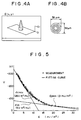
- Fig. 3A is a graph showing the energy distribution (beam profile) of the light beam irradiating the photosensitive member 6.
- Fig. 4A is a graph showing the exposure distribution on the photosensitive member 6.
- the diameter of the light beam at 1/e 2 with respect to the peak of the exposure distribution is 30 ⁇ m in a main-scan direction, and 38 ⁇ m in a sub-scan direction (see Fig. 3B).
- the energy distribution of the light beam represents the Gaussian distribution of 30 ⁇ m in the main-scan direction and 38 ⁇ m in the sub-scan direction.
- the exposure diameter of the light beam in the exposure distribution is 38 ⁇ m both in the main-scan direction and the sub-scan direction (see Fig. 4B).
- the Gaussian distribution is approximately 38 ⁇ m both in the main-scan direction and the sub-scan direction. Accordingly, the exposure diameter Db of the light beam defined as the minimum diameter at 1/e 2 with respect to the peak of the exposure distribution is 38 ⁇ m.
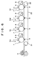
- Fig. 5 is a graph showing damping characteristics of the surface potential V of the photosensitive member 6 with respect to the exposure E.
- the image exposure unit 11 of this embodiment emits a light beam having a wavelength of 670 nm, and its exposure power is adjusted to 0.23 mW on the surface of the photosensitive member 6.
- the exposure at the peak of the exposure distribution i.e., the maximum exposure within the exposure diameter Db, can be a value which makes the differential sensitivity of the photosensitive layer 12 small enough.
- the "value that makes the differential sensitivity small enough” refers to the value of the exposure E that can produce gray-level images by the gray-level image device by virtue of the damping characteristics of the photosensitive member to obtain high-precision and stable images.
- the "value that makes the differential sensitivity small enough” is, for instance, a value to lower the differential sensitivity of the photosensitive layer 12 to a third of its maximum value or even less.
- the maximum differential sensitivity (dVmax) is 28 V ⁇ m 2 /mJ
- the exposure E corresponding to a differential sensitivity which is a third of its maximum value or less is the value that makes the differential sensitivity small enough.
- the peak exposure Epeak at the peak of the exposure distribution is 21 mL/m 2
- the corresponding differential sensitivity dVo is 5 V ⁇ m 2 /mJ. This is approximately a fifth of the maximum differential sensitivity.
- the charging unit 7 charges the photosensitive layer 12 on the photosensitive member 6, and an electrostatic latent image is formed at the exposure point EX on the charged photosensitive member 6 based on the image information.
- the gray-level image device reproduces the gray-level in accordance with the gray-level information included in the image data. Toners supplied from the developing unit 8 are applied to the electrostatic latent image, thereby developing the image.
- the developed image i.e., the toner image, is then transferred onto a transfer sheet 1 transported to the electrophotographic processing unit 5 at a predetermined pace.
- the fixing unit 4 fixes the transferred image, thereby completing the image formation on the transfer sheet 1.
- the cleaning unit 10 cleans the photosensitive member 6 to remove the residual toners.
- the maximum exposure within the exposure diameter Db of the light beam is set at a value that makes the differential sensitivity of the photosensitive layer 12 small enough.
- high-quality image formation can be performed without being adversely affected by mechanical vibration and others.
- the damping characteristics of the photosensitive body 6 shown in Fig. 5 exposure is performed in the area where the differential sensitivity is small. Because of this, a fluctuation in the surface potential of the photosensitive member 6 caused by a fluctuation of the exposure E is small.
- the exposure E fluctuates due to mechanical vibration or operational instability in the components, the fluctuation in the surface potential of the photosensitive member 6 is small, and high-precision and stable image formation can be carried out.
- the relationship between the thickness Tp of the photosensitive layer 12 and the exposure diameter Db is 2Tp ⁇ Db, the charge diffusion and electric field on the photosensitive layer 12 of the photosensitive member 6 are small. This prevents adverse influence from mechanical vibration or fluctuations, and a blur of an electrostatic latent image can be avoided.
- high-precision and stable image formation can be performed with excellent gray-level image presentation.
- the value of the maximum exposure within the exposure diameter Db that makes the differential sensitivity of the photosensitive layer small enough is a value of the exposure that can utilize the damping characteristics of the photosensitive member 6 enough to obtain stability while producing a gray-level image. More specifically, the maximum exposure of this value lowers the differential sensitivity of the photosensitive layer 12 to a third of its maximum value. If the photosensitive member 6 is exposed with the exposure of this value, the exposed area of the photosensitive member 6 includes an area which is not completely saturable. Therefore, the gray-level image device can be operated not only by a dot area modulation method but also by a dot density modulation method.
- the thickness Tp of the photosensitive layer 12 and the exposure diameter Db is defined as 2Tp ⁇ Db, the charge diffusion and the electric field on the photosensitive layer of the photosensitive member are so small that the dots become fine. Thus, an excellent gray-level image can be produced by the dot area modulation method.
- the photosensitive member 6 which is an organic photosensitive member, has a poor mechanical strength, and is often subjected to abrasion by the cleaning unit 10.
- the layer thickness Tp of the photosensitive layer 12 and the exposure diameter Db of the light beam is defined as 8 Tp > Db in this embodiment, the layer thickness Tp of the photosensitive layer 12 does not become too thin.
- the life of the photosensitive member 6 can be prolonged, while the charge diffusion and the electric field on the photosensitive layer are restricted so as not to obstruct practical use.
- the exposure diameter Db of the light beam in this embodiment is 38 ⁇ m. So, even if a sufficient light energy is given to the photosensitive member 6, the diameter of each pixel actually formed on the transfer sheet 1 is in the range of 50 to 70 ⁇ m, which is the resolution of the eye in the range of clear vision (25 to 30 cm). Thus, high-quality image formation is carried out.
- image formation may be performed by a positive development method. More specifically, the charging unit 7 uniformly charges the photosensitive member 6 with the polarity reverse to the toners contained in the developing unit 8, and an electrostatic latent image is formed in the non-exposed area by the image exposure unit 11. The developing unit 8 then applies toners to the electrostatic latent image.
- the maximum exposure within the exposure diameter Db is set at the value that makes the differential sensitivity of the photosensitive layer 12, and the dots in the electrostatic latent image in the formed non-exposed area are fine. Thus, fine image formation can be performed. As the non-exposed area becomes a solid portion, the image density in the non-exposed portion is high enough.
- the charging unit 7 When performing image formation by the positive development method, the charging unit 7 positively charges the surface of the photosensitive member 6 by utilizing the corona discharge of the charging unit 7. By doing so, the photosensitive member 6 is more steadily charged. Furthermore, negative toners, which are widely used, can be used in this embodiment.
- the error diffusion method and the dither method have been mentioned above as examples of the gray-tone level image presenting method using the gray-level image device, but the dot area modulation method as well as the dot density modulation method can also be employed.
- an inorganic photosensitive member made of amorphous silicon is used for the photosensitive member 6.
- the charging unit 7 positively charges the photosensitive member 6, for instance, at +550 V.
- the image exposure unit 11 forms an electrostatic latent image by exposing the surface of the photosensitive member 6 with a light beam having a light energy more than twice larger than the light energy that can cause the surface potential of the uniformly charged photosensitive member 6 to damp to a half of its potential.
- the electric potential in the exposed area on the photosensitive member 6 is +50 V, for instance.
- the developing unit 8 contains negative toners, and is biased at +200 V to develop an electrostatic latent image formed on the photosensitive member 6 by a positive development method.
- the charging unit 7 uniformly charges the photosensitive member 6 with positive polarity (at +550 V, for instance), which is the reverse polarity to the toners contained in the developing unit 8.
- the uniformly charged photosensitive member 6 is them exposed by the image exposure unit 11, so that an electrostatic latent image of + 550 V is formed in the non-exposed area where the potential drops to +50 V.
- the electrostatic latent image has the polarity reverse to the toners contained in the developing unit 8, and the potential difference is large.
- the transferring unit 9 then transfers the toner image onto a transfer sheet 1, thereby completing image formation on the transfer sheet 1.
- the image exposure unit 11 forms an electrostatic latent image by exposing the surface of the photosensitive member 6 with a light beam having a light energy more than twice larger than a light energy which can cause the surface potential of the uniformly charged photosensitive member 6 to a half of its potential.
- the exposure is carried out in the saturation range or in the neighborhood of the saturation range of the photosensitive member 6.
- the electrostatic latent image thus formed is developed by the positive development method. Accordingly, the combination of the positive development method and the exposure within the neighborhood of the saturation range of the photosensitive member 6 further improves the fineness of the dots. Thus, fine image formation can be performed.
- the non-exposed area forms a solid image, the image density in the non-exposed area is high enough. Since the exposure is carried out in the saturation range or in the neighborhood of the saturation range of the photosensitive member 6, adverse influence of mechanical fluctuations can be avoided, and high-precision and stable image formation can be carried out.
- the image exposure unit 11 forms an electrostatic image by exposing the surface of the photosensitive member 6 with a light beam having a light energy more than twice larger than the light energy that can cause the surface potential of the uniformly charged photosensitive member 6 to damp to a half of its potential.
- the photosensitive member 6 is exposed in the neighborhood of the saturation range.
- a dot density modulation method may be employed, as well as a dot area modulation method, to produce a gray-level image.
- the combination of the positive development method and the exposure in the neighborhood of the saturation range of the photosensitive member 6 further improves the fineness of the dots. This enables fine gray-level image formation by the dot area modulation method.
- high-precision and stable image formation can be carried out, while fine gray-level image presentation is maintained.
- the charging unit 7 positively charges the surface of the photosensitive member 6. If the charging unit 7 is of a type that utilizes corona discharge, the photosensitive member 6 can be more stably charged. Negative toners that are widely used can be used too.
- an inorganic photosensitive member made of amorphous silicon is used for the photosensitive member 6, the life of the photosensitive member 6 is prolonged, and its security is improved.
- This embodiment is an example of the present invention applied to a tandem-type color image forming apparatus.
- Image processing units 5Y, 5M, 5C, and 5K for yellow, magenta, cyan, and black, respectively, are arranged in that order from the upstream side on a transportation belt 23 stretched over a drive roller 21 and a follow roller 22.
- the image processing unit 5 of the first and second embodiments is employed if appropriate.
- a transfer sheet 1 fed from a feeding unit 2 (not shown in Fig.
- image processing unit 5 of the first and second embodiments With the image processing unit 5 of the first and second embodiments, high-precision and stable image formation, fine dots, and precise gray-level images can be obtained. Such features of the image processing unit 5 are advantageous in the color image apparatus to form high-quality color images.
- the diameter of the photosensitive member 6 is 100 mm, and the layer thickness Tp of the photosensitive layer 12 is 13 ⁇ m.
- the light damping characteristics with respect to a light of 670 nm are as shown in the graph of Fig. 5.
- the maximum differential sensitivity is 28 V ⁇ m 2 /mJ.
- This photosensitive member 6 is rotated at a peripheral speed (process speed) of 20 mm/sec.
- the charging unit 7 charges the photosensitive member 6 at -340 V.
- the developing unit 8 uses a developer, which is a 5 wt% mixture of silicon ferrite carriers of 50 ⁇ m in mean particle size and toners of 7 ⁇ m in mean particle size.
- the mean charge amount of the toners measured by a blowoff device is -20 ⁇ c/g.
- the developing unit 8 develops an image by rotating a developing sleeve, to which a bias voltage of -200 V is applied, at a periphery speed of 40 mm/sec.
- the light beam emitted from the image exposure unit 11 is 670 nm in wavelength as in the embodiments of the present invention, and the exposure power on the surface of the photosensitive member 6 is adjusted at 0.23 mW.
- the exposure diameter Db is adjusted so that the Gaussian distribution indicates 30 ⁇ m in the main-scan direction and 38 ⁇ m in the sub-scan direction, as shown in Fig. 3B.
- a polygonal mirror having eight planes is employed and rotated at 7200 rpm.
- the surface of the photosensitive member 6 is then scanned by the light beam at 530 m/sec. In this manner, the image exposure unit 11 exposes the photosensitive member 6 by 40 nsec (approximately 20 ⁇ m in length on the photosensitive member 6).
- the Gaussian distribution indicates concentric circles of 38 ⁇ m both in the main-scan direction and the sub-scan direction. Accordingly, the exposure diameter Db is 38 ⁇ m, as shown in Fig. 4B.
- the peak value in the exposure distribution i.e., the peak exposure
- the differential sensitivity indicates 5 V ⁇ m 2 /mJ, which is a fifth of the value of the maximum differential sensitivity or smaller.
- the surface potential of the photosensitive member 6 is -40 V.
- the mean particle size of the toners in a toner image formed on the surface of the photosensitive member 6 is 37 ⁇ m, and its standard deviation is 5 ⁇ m. This means that uniform pixels are obtained. Even if the charge potential, the development bias, and the exposure amount are changed by 30% each, the uniformity in the pixels is maintained.
- the apparatus in this example can perform high-precision and stable image formation.
- the diameter of the photosensitive member 6 is 120 mm, and the layer thickness Tp of the photosensitive layer 12 is 17 ⁇ m.
- the light damping characteristics with respect to a light of 670 nm are as shown in the graph of Fig. 5.
- the maximum differential sensitivity is 50 V ⁇ m 2 /mJ.
- This photosensitive member 6 is rotated at a peripheral speed (process speed) of 180 mm/sec.
- the charging unit 7 charges the photosensitive member 6 at -500 V.
- the developing unit 8 uses a developer, which is a 5 wt% mixture of silicon ferrite carriers of 50 ⁇ m in mean particle size and toners of 7 ⁇ m in mean particle size.
- the mean charge amount of the toners measured by a blowoff device is -20 ⁇ c/g.
- the developing unit 8 develops an image by rotating a developing sleeve, to which a bias voltage of -200 V is applied, at a periphery speed of 40 mm/sec.
- the light beam emitted from the image exposure unit 11 is 670 nm in wavelength as in the embodiments of the present invention, and the exposure power on the surface of the photosensitive member 6 is adjusted at 1.63 mW.
- the exposure diameter Db is adjusted so that the Gaussian distribution indicates 55 ⁇ m in the main-scan direction and 85 ⁇ m in the sub-scan direction, as shown in Fig. 3B.
- a polygonal mirror having eight planes is employed and rotated at 21260 rpm.
- the surface of the photosensitive member 6 is then scanned by the light beam at 870 m/sec. In this manner, the image exposure unit 11 exposes the photosensitive member 6 by 55 nsec (approximately 50 ⁇ m in length on the photosensitive member 6).
- the Gaussian distribution indicates concentric circles of 80 ⁇ m both in the main-scan direction and the sub-scan direction. Accordingly, the exposure diameter Db is 80 ⁇ m, as shown in Fig. 4B.
- the peak value in the exposure distribution i.e., the peak exposure
- the differential sensitivity sufficiently drops to 5 V ⁇ m 2 /mJ.
- the surface potential of the photosensitive member 6 is -50 V.
- the mean particle size of the toners in a toner image formed on the surface of the photosensitive member 6 is 60 ⁇ m, and its standard deviation is 5 ⁇ m. This means that uniform pixels are obtained. Even if the charge potential, the development bias, and the exposure amount are changed by 20% each, the uniformity in the pixels is maintained.
- the apparatus in this example can perform high-precision and stable image formation.
- the relationship between the layer thickness Tp of the photosensitive layer on the photosensitive member and the exposure diameter Db of the light beam irradiating the photosensitive member is defined as 2Tp ⁇ Db, so that the charge diffusion and electric field in the photosensitive layer on the photosensitive member can be reduced.
- the maximum exposure within the exposure diameter Db is set at a value that can sufficiently reduce the differential sensitivity of the photosensitive layer, or at a value that can reduce the differential sensitivity to a third of its maximum value or smaller.
- high-quality image formation can be carried out regardless of mechanical fluctuations. In this manner, high-precision and stable image formation is performed, and excellent gray-level images are produced.
- an organic photosensitive member having a photosensitive layer made of an organic substance is used for the photosensitive member.
- the relationship between the layer thickness Tp of the photosensitive layer and the exposure diameter of the light beam is defined as 8Tp > Db. Accordingly, although the organic photosensitive member is poor in methcanical strength, the layer thickness Tp of the photosensitive layer 12 does not become too thin. Thus, the life of the photosensitive member 6 can be prolonged, while the charge diffusion and the electric field on the photosensitive layer are restricted so as not to obstruct practical use.
- the exposure diameter Db of the light beam is 30 to 50 ⁇ m.
- the resolution of the eye is 50 to 70 ⁇ m in the range of clear vision (25 to 30 cm).
- the exposure diameter in the electrophotographic process is set at 30 to 50 ⁇ m, so that the pixel size in an electrostatic latent image on the photosensitive member is 40 to 60 ⁇ m even if a sufficient light energy is given to the photosensitive member 6.
- the diameter of each pixel actually formed on the transfer sheet 1 is 50 to 70 ⁇ m, which is the resolution of the eye in the range of clear vision (25 to 30 cm).
- the developing unit develops an electrostatic latent image by a positive development method.
- the charging unit uniformly charges the photosensitive member with the polarity reverse to the polarity of the charged toners contained in the developing unit.
- the exposure unit exposes the photosensitive member so as to form an electrostatic latent image in the non-exposed area.
- the toners adhere to the electrostatic latent image, i.e., the non-exposed area on the photosensitive member, to form an image.
- the maximum exposure in the neighborhood of the saturation range i.e., the maximum exposure within the exposure diameter Db
- the maximum exposure in the neighborhood of the saturation range is set at a value that makes the differential sensitivity of the photosensitive layer small enough, for instance, a third of its maximum value or smaller. This often causes dots to grow in size in the exposed area.
- the dots can be reduced in size, because an electrostatic latent image is formed in the non-exposed area.
- fine image formation is carried out.
- the non-exposed area is a solid portion, the image density in the non-exposed area is high.
- the charging unit positively charges the surface of the photosensitive member.
- a charging unit that utilizes corona discharge charges the photosensitive member even more stably.
- negative toners which are widely used, can be employed.
- the image forming apparatus of the present invention comprises: the photosensitive member having the photosensitive layer on its surface; the charging unit for uniformly charging the surface of the photosensitive member; the image exposure unit for exposing the photosensitive member with a light beam having a light energy more than twice larger than the light energy that reduces the surface potential of the uniformly charged photosensitive member to a half of its potential; the developing unit for developing an electrostatic latent image formed on the photosensitive member by a positive development method; and the transferring unit for transferring a developed image from a photosensitive member onto a recording medium.
- the charging unit uniformly charges the photosensitive member with the reverse polarity to the polarity of the charged toners contained in the developing unit.
- the exposure unit exposes the photosensitive member to form an electrostatic latent image in the non-exposed area.
- the toners adhere to the electrostatic latent image to form an image.
- the image exposure unit exposes the photosensitive member with a light beam having a light energy more than twice larger than the light energy that reduces the surface potential of the uniformly charged photosensitive member to a half of its potential.
- the exposure is carried out in the saturation range or in the neighborhood of the saturation range of the photosensitive member. This often causes the dots to grow in size in the exposed area.
- an electrostatic latent image is formed in the non-exposed area, and the exposure is carried out within the neighborhood of the saturation area. In this manner, the dots can be reduced in size. Thus, fine image formation is carried out. Also, as the non-exposed area is a solid portion, the image density in the non-exposed area is high enough. Since the exposure is carried out in the saturation range or in the neighborhood of the saturation range on the photosensitive member, high-precision and stable image formation is carried out regardless of mechanical fluctuations.
- the charging unit positively charges the surface of the photosensitive member.
- a charging unit that utilizes corona discharge can charge the photosensitive member in a more stable manner.
- negative toners which are widely used, can be employed.
- an inorganic photosensitive member made of amorphous silicon is used for the photosensitive member.
- the life of the photosensitive member is prolonged, and its security is improved.
- the image forming apparatus of the present invention comprises a gray-level image device which transmits a drive signal to the image exposure unit, and presents a gray-level image in accordance with a gray-level signal based on image data having gray-level information.
- an electrostatic latent image is formed by exposing the photosensitive member with a light beam more than twice larger than the light energy that can reduce the surface potential of the uniformly charged photosensitive member to a half of its potential.
- the photosensitive member is exposed in a region which has not reached the saturation range, and the gray-level image device can be operated not only by a dot area modulation method but also by a dot density modulation method.
- the combination of the positive development method for developing an electrostatic image formed in the non-exposed area and the exposure in the saturation range or in the neighborhood of the saturation range of the photosensitive member helps to obtain fine dots.
- fine gray-level image presentation is possible by the dot area modulation method.
- a color image is formed with at least three colors: yellow, magenta, and cyan. High-precision and stable image formation, the fineness of the dots, and excellent gray-level presentation are all even more advantageous in color image formation.
Priority Applications (1)
| Application Number | Priority Date | Filing Date | Title |
|---|---|---|---|
| EP05006372A EP1548514B1 (fr) | 1996-10-08 | 1997-10-06 | Appareil de formation d'image et procédé de formation d'image |
Applications Claiming Priority (5)
| Application Number | Priority Date | Filing Date | Title |
|---|---|---|---|
| JP26645796 | 1996-10-08 | ||
| JP26645796 | 1996-10-08 | ||
| JP23805797 | 1997-09-03 | ||
| JP9238057A JPH10171221A (ja) | 1996-10-08 | 1997-09-03 | 画像形成装置及び画像形成方法 |
| PCT/JP1997/003555 WO1998015875A1 (fr) | 1996-10-08 | 1997-10-06 | Dispositif et procede de formation d'image |
Related Child Applications (1)
| Application Number | Title | Priority Date | Filing Date |
|---|---|---|---|
| EP05006372A Division EP1548514B1 (fr) | 1996-10-08 | 1997-10-06 | Appareil de formation d'image et procédé de formation d'image |
Publications (3)
| Publication Number | Publication Date |
|---|---|
| EP0932085A1 true EP0932085A1 (fr) | 1999-07-28 |
| EP0932085A4 EP0932085A4 (fr) | 2002-04-10 |
| EP0932085B1 EP0932085B1 (fr) | 2005-05-25 |
Family
ID=26533512
Family Applications (2)
| Application Number | Title | Priority Date | Filing Date |
|---|---|---|---|
| EP05006372A Expired - Lifetime EP1548514B1 (fr) | 1996-10-08 | 1997-10-06 | Appareil de formation d'image et procédé de formation d'image |
| EP97942248A Expired - Lifetime EP0932085B1 (fr) | 1996-10-08 | 1997-10-06 | Dispositif et procede de formation d'image |
Family Applications Before (1)
| Application Number | Title | Priority Date | Filing Date |
|---|---|---|---|
| EP05006372A Expired - Lifetime EP1548514B1 (fr) | 1996-10-08 | 1997-10-06 | Appareil de formation d'image et procédé de formation d'image |
Country Status (5)
| Country | Link |
|---|---|
| US (1) | US6249304B1 (fr) |
| EP (2) | EP1548514B1 (fr) |
| JP (1) | JPH10171221A (fr) |
| DE (1) | DE69733358T2 (fr) |
| WO (1) | WO1998015875A1 (fr) |
Cited By (1)
| Publication number | Priority date | Publication date | Assignee | Title |
|---|---|---|---|---|
| EP1079597A2 (fr) * | 1999-08-20 | 2001-02-28 | Sharp Kabushiki Kaisha | Dispositif de formation d'image |
Families Citing this family (68)
| Publication number | Priority date | Publication date | Assignee | Title |
|---|---|---|---|---|
| JP2007256970A (ja) * | 1999-06-25 | 2007-10-04 | Ricoh Co Ltd | 画像形成装置 |
| JP3825600B2 (ja) * | 2000-01-13 | 2006-09-27 | 株式会社リコー | 帯電装置、画像形成装置、像担持体ユニット及び荷電ローラ |
| CN1900837B (zh) | 2000-02-17 | 2012-10-03 | 株式会社理光 | 墨粉收纳容器、补给墨粉的方法及墨粉补给装置 |
| JP3849971B2 (ja) | 2000-03-16 | 2006-11-22 | 株式会社リコー | 劣化状態確認可能な製品 |
| US6591077B2 (en) | 2000-05-08 | 2003-07-08 | Ricoh Company, Ltd. | Image forming apparatus and toner container therefor |
| JP4190160B2 (ja) | 2000-06-05 | 2008-12-03 | 株式会社リコー | 画像形成装置 |
| JP2002091123A (ja) | 2000-07-14 | 2002-03-27 | Ricoh Co Ltd | カラー画像形成装置およびトナー補給装置 |
| ATE375772T1 (de) * | 2000-07-18 | 2007-11-15 | Coloplast As | Wundverband |
| EP1752837B1 (fr) | 2000-09-26 | 2015-03-11 | Ricoh Company, Ltd. | Appareil de formation des images. |
| EP1739499B1 (fr) | 2000-09-27 | 2011-11-02 | Ricoh Company, Ltd. | Appareil de formation d'images en couleur, méthode de type tandem de formation d'images en couleur et méthode de formation d'images en couleur |
| JP3958511B2 (ja) * | 2000-09-28 | 2007-08-15 | 株式会社リコー | トナー補給装置および画像形成装置 |
| JP2002174939A (ja) | 2000-09-29 | 2002-06-21 | Ricoh Co Ltd | 画像形成装置 |
| JP2003005608A (ja) | 2000-10-18 | 2003-01-08 | Ricoh Co Ltd | 像担持体上の付着物除去方法およびその方法を用いる画像形成装置 |
| JP3734735B2 (ja) * | 2000-11-02 | 2006-01-11 | 株式会社リコー | 電子写真感光体 |
| EP1205808B1 (fr) * | 2000-11-08 | 2010-03-17 | Ricoh Company, Ltd. | Photorécepteur électrophotographique, procédé pour sa fabrication, ainsi que procédé et appareil de production d' image utilisant le photorécepteur |
| US6542707B2 (en) | 2000-11-13 | 2003-04-01 | Ricoh Co., Ltd. | Method and apparatus for image forming capable of effectively transferring various kinds of powder |
| JP2002278269A (ja) | 2000-12-20 | 2002-09-27 | Ricoh Co Ltd | 画像形成装置 |
| US6665508B2 (en) | 2001-01-31 | 2003-12-16 | Ricoh Company, Ltd. | Toner container and image forming apparatus using the same |
| US6597883B2 (en) | 2001-02-13 | 2003-07-22 | Ricoh Company, Ltd. | Powder pump capable of effectively conveying powder and image forming apparatus using powder pump |
| JP2002244488A (ja) | 2001-02-13 | 2002-08-30 | Ricoh Co Ltd | 潜像担持体および画像形成装置 |
| JP2002341572A (ja) | 2001-02-20 | 2002-11-27 | Ricoh Co Ltd | 画像形成装置、画像形成方法、感光体及びその製造方法並びに画像形成用プロセスカートリッジ |
| JP2002347976A (ja) | 2001-03-21 | 2002-12-04 | Ricoh Co Ltd | 用紙搬送装置、画像形成装置および画像形成システム |
| JP3854171B2 (ja) | 2001-03-22 | 2006-12-06 | 株式会社リコー | 感光体リサイクル装置、感光体リサイクル方法 |
| US6677091B2 (en) | 2001-03-22 | 2004-01-13 | Ricoh Company, Ltd. | Electrophotographic photoreceptor and electrophotographic apparatus |
| US6777149B2 (en) * | 2001-03-23 | 2004-08-17 | Ricoh Company Limited | Electrophotographic image forming apparatus and process cartridge, and electrophotographic photoreceptor therefor |
| US6936388B2 (en) | 2001-03-23 | 2005-08-30 | Ricoh Company, Ltd. | Electrophotographic photoreceptor, and image forming method, image forming apparatus, and image forming apparatus processing unit using same |
| JP2002351287A (ja) | 2001-03-23 | 2002-12-06 | Ricoh Co Ltd | 作像ユニット及び画像形成装置 |
| EP1253480B1 (fr) | 2001-04-27 | 2011-01-05 | Ricoh Company, Ltd. | Dispositif de formation d'images avec alimentation en toner améliorée |
| DE60229995D1 (de) | 2001-05-01 | 2009-01-08 | Ricoh Kk | Elektrophotographischer Photorezeptor, Herstellungsverfahren und Bilderzeugungsvorrichtung |
| JP2003043862A (ja) * | 2001-05-23 | 2003-02-14 | Ricoh Co Ltd | 潜像担持体及び画像形成装置ならびに制振部材 |
| US6939651B2 (en) * | 2001-06-21 | 2005-09-06 | Ricoh Company, Ltd. | Electrophotographic photoconductor, and process cartridge and electrophotographic apparatus using the same |
| JP3966543B2 (ja) | 2001-06-25 | 2007-08-29 | 株式会社リコー | 電子写真画像形成方法及び電子写真装置 |
| EP1271259B1 (fr) | 2001-06-26 | 2013-11-20 | Ricoh Company, Ltd. | Appareil de formation d'images et unité de traitement associée |
| US6830858B2 (en) * | 2001-06-27 | 2004-12-14 | Ricoh Company, Ltd. | Electrophotographic photosensitive member, preparation method thereof, image forming process, apparatus and process cartridge using the same |
| US6803162B2 (en) | 2001-07-26 | 2004-10-12 | Ricoh Company, Ltd. | Electrophotographic image forming apparatus, photoreceptor therefor and method for manufacturing the photoreceptor |
| JP4121333B2 (ja) * | 2001-08-27 | 2008-07-23 | 株式会社リコー | 画像形成装置,プログラム更新方法および記録媒体 |
| JP4083505B2 (ja) | 2001-08-27 | 2008-04-30 | 株式会社リコー | 画像形成装置,プログラム更新方法および記録媒体 |
| JP4212849B2 (ja) | 2001-08-31 | 2009-01-21 | 株式会社リコー | 画像形成装置 |
| DE60239439D1 (de) * | 2001-09-06 | 2011-04-28 | Ricoh Co Ltd | Elektrophotografischer Photorezeptor, Bildaufzeichnungsmethode, Bildaufzeichnungsgerät, und Prozesskartusche |
| US6800410B2 (en) * | 2001-10-02 | 2004-10-05 | Ricoh Company, Ltd. | Image forming apparatus |
| JP3920616B2 (ja) * | 2001-10-04 | 2007-05-30 | 株式会社リコー | 転写装置および画像形成装置 |
| JP4043337B2 (ja) * | 2001-11-30 | 2008-02-06 | 株式会社リコー | 画像形成方法及びこの方法を用いる画像形成装置 |
| JP2003241570A (ja) | 2001-12-11 | 2003-08-29 | Ricoh Co Ltd | 画像形成装置 |
| JP2004050515A (ja) * | 2002-07-17 | 2004-02-19 | Ricoh Co Ltd | 画像形成装置 |
| EP1431838B1 (fr) * | 2002-09-13 | 2010-02-10 | Ricoh Company, Ltd. | Dispositif de chargement avec un rouleau de chargement et appareil de formation d'images l'utilisant |
| JP2004133419A (ja) * | 2002-09-20 | 2004-04-30 | Ricoh Co Ltd | 画像形成装置・転写ユニット |
| EP1437631B1 (fr) * | 2002-11-29 | 2008-09-10 | Ricoh Company, Ltd. | Méthode pour déterminer la surface de mésure minimal utilisable d'un capteur de detection d'un motif d'alignement dans un appareil de formation d'image |
| JP4330112B2 (ja) * | 2002-12-09 | 2009-09-16 | 株式会社リコー | カラー画像形成装置 |
| JP4462917B2 (ja) * | 2003-01-23 | 2010-05-12 | 株式会社リコー | 光ビーム書込装置、画像形成装置、画像補正方法 |
| JP2004287403A (ja) * | 2003-02-26 | 2004-10-14 | Ricoh Co Ltd | 画像形成装置、画像位置ずれ補正方法および記憶媒体 |
| US20040251435A1 (en) * | 2003-04-07 | 2004-12-16 | Noboru Sawayama | Optical sensor and image forming apparatus |
| US7203433B2 (en) * | 2003-06-25 | 2007-04-10 | Ricoh Company, Ltd. | Apparatus for detecting amount of toner deposit and controlling density of image, method of forming misalignment correction pattern, and apparatus for detecting and correcting misalignment of image |
| JP4778671B2 (ja) * | 2003-07-02 | 2011-09-21 | 株式会社リコー | 画像形成装置に用いる転写用部材の抵抗変化判定方法 |
| JP2005148665A (ja) | 2003-11-20 | 2005-06-09 | Ricoh Co Ltd | 帯電装置及びこれを用いた画像形成装置 |
| JP2006259639A (ja) * | 2005-03-18 | 2006-09-28 | Ricoh Co Ltd | 画像形成装置 |
| JP4643324B2 (ja) | 2005-03-18 | 2011-03-02 | 株式会社リコー | 画像形成装置 |
| JP2007187700A (ja) * | 2006-01-11 | 2007-07-26 | Ricoh Co Ltd | 転写装置、画像形成装置 |
| JP2008008923A (ja) * | 2006-06-27 | 2008-01-17 | Ricoh Co Ltd | 画像形成装置及びプロセスカートリッジ |
| US8422903B2 (en) * | 2007-05-01 | 2013-04-16 | Ricoh Company, Ltd. | Image forming apparatus and image forming method |
| JP5268020B2 (ja) | 2008-10-22 | 2013-08-21 | 株式会社リコー | 画像形成装置 |
| JP5392126B2 (ja) * | 2010-02-05 | 2014-01-22 | 富士ゼロックス株式会社 | 画像形成装置、画像形成制御装置、及びプログラム |
| JP5614067B2 (ja) * | 2010-03-18 | 2014-10-29 | 富士ゼロックス株式会社 | 露光装置及び画像形成装置 |
| JP6069983B2 (ja) | 2012-09-10 | 2017-02-01 | 株式会社リコー | 画像形成装置 |
| JP6213045B2 (ja) | 2013-08-21 | 2017-10-18 | 株式会社リコー | 光走査装置、画像形成装置、及び光走査方法 |
| JP6481439B2 (ja) | 2015-03-18 | 2019-03-13 | 株式会社リコー | 走査装置及び画像形成装置 |
| JP2018155854A (ja) | 2017-03-16 | 2018-10-04 | 株式会社リコー | 画像形成装置 |
| JP2021039285A (ja) | 2019-09-04 | 2021-03-11 | 株式会社リコー | 画像形成装置、及び画像形成方法 |
| US11880155B2 (en) | 2021-11-25 | 2024-01-23 | Ricoh Company, Ltd. | Image forming apparatus, transfer device, and storage medium |
Citations (6)
| Publication number | Priority date | Publication date | Assignee | Title |
|---|---|---|---|---|
| EP0464349A2 (fr) * | 1990-05-21 | 1992-01-08 | Konica Corporation | Appareil et procédé de formation d'image |
| US5153609A (en) * | 1989-05-09 | 1992-10-06 | Canon Kabushiki Kaisha | Image forming apparatus |
| JPH05216330A (ja) * | 1992-02-03 | 1993-08-27 | Hitachi Ltd | 電子写真装置 |
| EP0690357A1 (fr) * | 1994-06-30 | 1996-01-03 | Canon Kabushiki Kaisha | Appareil électrographique et méthode pour la formation d'image |
| EP0706097A2 (fr) * | 1994-10-03 | 1996-04-10 | Canon Kabushiki Kaisha | Procédé de formation d'images |
| EP0716536A2 (fr) * | 1994-12-07 | 1996-06-12 | Canon Kabushiki Kaisha | Appareil de formation d'image et cartouche de traitement |
Family Cites Families (10)
| Publication number | Priority date | Publication date | Assignee | Title |
|---|---|---|---|---|
| JPS5683757A (en) | 1979-12-11 | 1981-07-08 | Fujitsu Ltd | Electrophotographic type two-color copy recording method |
| JPS56165162A (en) | 1980-05-26 | 1981-12-18 | Minolta Camera Co Ltd | Electrophotographic copying method |
| US5172132A (en) * | 1990-03-06 | 1992-12-15 | Konica Corporation | Digital image forming device and method for forming an image from a plurality of dots |
| JP2959031B2 (ja) * | 1990-03-20 | 1999-10-06 | ミノルタ株式会社 | デジタル画像形成法 |
| JPH0463373A (ja) * | 1990-07-03 | 1992-02-28 | Konica Corp | 画像形成方法 |
| JPH04288248A (ja) * | 1990-08-20 | 1992-10-13 | Kyocera Corp | 画像形成方法 |
| JPH05127498A (ja) * | 1991-11-06 | 1993-05-25 | Konica Corp | 画像形成装置 |
| EP0716348B1 (fr) * | 1994-12-07 | 2000-09-06 | Canon Kabushiki Kaisha | Elément photosensible électrophotographique, appareil électrophotographique et cassette de traitement l'utilisant |
| JPH08272197A (ja) * | 1994-12-07 | 1996-10-18 | Canon Inc | 画像形成装置及びプロセスカートリッジ |
| JPH08286407A (ja) * | 1995-04-18 | 1996-11-01 | Konica Corp | 画像形成方法及び装置 |
-
1997
- 1997-09-03 JP JP9238057A patent/JPH10171221A/ja active Pending
- 1997-10-06 EP EP05006372A patent/EP1548514B1/fr not_active Expired - Lifetime
- 1997-10-06 EP EP97942248A patent/EP0932085B1/fr not_active Expired - Lifetime
- 1997-10-06 DE DE69733358T patent/DE69733358T2/de not_active Expired - Lifetime
- 1997-10-06 WO PCT/JP1997/003555 patent/WO1998015875A1/fr active IP Right Grant
- 1997-10-06 US US09/269,750 patent/US6249304B1/en not_active Expired - Lifetime
Patent Citations (6)
| Publication number | Priority date | Publication date | Assignee | Title |
|---|---|---|---|---|
| US5153609A (en) * | 1989-05-09 | 1992-10-06 | Canon Kabushiki Kaisha | Image forming apparatus |
| EP0464349A2 (fr) * | 1990-05-21 | 1992-01-08 | Konica Corporation | Appareil et procédé de formation d'image |
| JPH05216330A (ja) * | 1992-02-03 | 1993-08-27 | Hitachi Ltd | 電子写真装置 |
| EP0690357A1 (fr) * | 1994-06-30 | 1996-01-03 | Canon Kabushiki Kaisha | Appareil électrographique et méthode pour la formation d'image |
| EP0706097A2 (fr) * | 1994-10-03 | 1996-04-10 | Canon Kabushiki Kaisha | Procédé de formation d'images |
| EP0716536A2 (fr) * | 1994-12-07 | 1996-06-12 | Canon Kabushiki Kaisha | Appareil de formation d'image et cartouche de traitement |
Non-Patent Citations (2)
| Title |
|---|
| PATENT ABSTRACTS OF JAPAN vol. 017, no. 658 (P-1654), 6 December 1993 (1993-12-06) & JP 05 216330 A (HITACHI LTD), 27 August 1993 (1993-08-27) * |
| See also references of WO9815875A1 * |
Cited By (2)
| Publication number | Priority date | Publication date | Assignee | Title |
|---|---|---|---|---|
| EP1079597A2 (fr) * | 1999-08-20 | 2001-02-28 | Sharp Kabushiki Kaisha | Dispositif de formation d'image |
| EP1079597A3 (fr) * | 1999-08-20 | 2003-10-29 | Sharp Kabushiki Kaisha | Dispositif de formation d'image |
Also Published As
| Publication number | Publication date |
|---|---|
| WO1998015875A1 (fr) | 1998-04-16 |
| DE69733358T2 (de) | 2006-01-26 |
| JPH10171221A (ja) | 1998-06-26 |
| DE69733358D1 (de) | 2005-06-30 |
| EP1548514A1 (fr) | 2005-06-29 |
| EP1548514B1 (fr) | 2012-06-06 |
| US6249304B1 (en) | 2001-06-19 |
| EP0932085A4 (fr) | 2002-04-10 |
| EP0932085B1 (fr) | 2005-05-25 |
Similar Documents
| Publication | Publication Date | Title |
|---|---|---|
| EP0932085B1 (fr) | Dispositif et procede de formation d'image | |
| JPH11112810A (ja) | 画像形成装置及びその制御方法及び記憶媒体 | |
| JP3616276B2 (ja) | 画像形成装置および画像形成方法 | |
| US6226019B1 (en) | Imaging forming apparatus for forming an image by digital processing | |
| JPH0576028B2 (fr) | ||
| JPH1158817A (ja) | 画像形成装置 | |
| EP1148709A2 (fr) | Appareil d'exposition pour la formation d'images et procédé de formation d'images | |
| JPH043312Y2 (fr) | ||
| JP3125192B2 (ja) | 画像形成方法 | |
| JP3892201B2 (ja) | 画像形成方法及び画像形成装置 | |
| JP2004106365A (ja) | 画像形成装置および複写装置 | |
| JP2000177171A (ja) | 画像形成装置及び画像形成方法 | |
| JPS6054567A (ja) | 記録装置 | |
| JP2002361922A (ja) | 画像形成装置 | |
| JP2003118161A (ja) | 画像形成装置 | |
| JP4588252B2 (ja) | 画像形成装置 | |
| JPH0420920A (ja) | 走査光学系及びこれを備える画像形成装置 | |
| JPH0463373A (ja) | 画像形成方法 | |
| JPH11105339A (ja) | 画像形成装置及び画像形成方法 | |
| JP2001215778A (ja) | 画像形成装置 | |
| JPH068525A (ja) | 多色画像形成装置 | |
| JPH05244372A (ja) | 画像形成装置 | |
| JPH0419612A (ja) | 走査光学系及びこれを利用する画像形成装置 | |
| JPH11291546A (ja) | 記録装置 | |
| JPH09281779A (ja) | 画像形成装置 |
Legal Events
| Date | Code | Title | Description |
|---|---|---|---|
| PUAI | Public reference made under article 153(3) epc to a published international application that has entered the european phase |
Free format text: ORIGINAL CODE: 0009012 |
|
| 17P | Request for examination filed |
Effective date: 19990407 |
|
| AK | Designated contracting states |
Kind code of ref document: A1 Designated state(s): DE ES FR GB IT NL |
|
| A4 | Supplementary search report drawn up and despatched |
Effective date: 20020227 |
|
| AK | Designated contracting states |
Kind code of ref document: A4 Designated state(s): DE ES FR GB IT NL |
|
| RIC1 | Information provided on ipc code assigned before grant |
Free format text: 7G 03G 13/04 A, 7G 03G 15/04 B, 7B 41J 2/44 B, 7H 04N 1/29 B |
|
| 17Q | First examination report despatched |
Effective date: 20021218 |
|
| GRAP | Despatch of communication of intention to grant a patent |
Free format text: ORIGINAL CODE: EPIDOSNIGR1 |
|
| GRAS | Grant fee paid |
Free format text: ORIGINAL CODE: EPIDOSNIGR3 |
|
| GRAA | (expected) grant |
Free format text: ORIGINAL CODE: 0009210 |
|
| AK | Designated contracting states |
Kind code of ref document: B1 Designated state(s): DE ES FR GB IT NL |
|
| PG25 | Lapsed in a contracting state [announced via postgrant information from national office to epo] |
Ref country code: NL Free format text: LAPSE BECAUSE OF FAILURE TO SUBMIT A TRANSLATION OF THE DESCRIPTION OR TO PAY THE FEE WITHIN THE PRESCRIBED TIME-LIMIT Effective date: 20050525 Ref country code: IT Free format text: LAPSE BECAUSE OF FAILURE TO SUBMIT A TRANSLATION OF THE DESCRIPTION OR TO PAY THE FEE WITHIN THE PRESCRIBED TIME-LIMIT;WARNING: LAPSES OF ITALIAN PATENTS WITH EFFECTIVE DATE BEFORE 2007 MAY HAVE OCCURRED AT ANY TIME BEFORE 2007. THE CORRECT EFFECTIVE DATE MAY BE DIFFERENT FROM THE ONE RECORDED. Effective date: 20050525 |
|
| REG | Reference to a national code |
Ref country code: GB Ref legal event code: FG4D |
|
| REF | Corresponds to: |
Ref document number: 69733358 Country of ref document: DE Date of ref document: 20050630 Kind code of ref document: P |
|
| PG25 | Lapsed in a contracting state [announced via postgrant information from national office to epo] |
Ref country code: ES Free format text: LAPSE BECAUSE OF FAILURE TO SUBMIT A TRANSLATION OF THE DESCRIPTION OR TO PAY THE FEE WITHIN THE PRESCRIBED TIME-LIMIT Effective date: 20050905 |
|
| NLV1 | Nl: lapsed or annulled due to failure to fulfill the requirements of art. 29p and 29m of the patents act | ||
| ET | Fr: translation filed | ||
| PLBE | No opposition filed within time limit |
Free format text: ORIGINAL CODE: 0009261 |
|
| STAA | Information on the status of an ep patent application or granted ep patent |
Free format text: STATUS: NO OPPOSITION FILED WITHIN TIME LIMIT |
|
| 26N | No opposition filed |
Effective date: 20060228 |
|
| REG | Reference to a national code |
Ref country code: FR Ref legal event code: PLFP Year of fee payment: 19 |
|
| REG | Reference to a national code |
Ref country code: FR Ref legal event code: PLFP Year of fee payment: 20 |
|
| PGFP | Annual fee paid to national office [announced via postgrant information from national office to epo] |
Ref country code: GB Payment date: 20161020 Year of fee payment: 20 Ref country code: DE Payment date: 20161020 Year of fee payment: 20 Ref country code: FR Payment date: 20161020 Year of fee payment: 20 |
|
| REG | Reference to a national code |
Ref country code: DE Ref legal event code: R071 Ref document number: 69733358 Country of ref document: DE |
|
| REG | Reference to a national code |
Ref country code: GB Ref legal event code: PE20 Expiry date: 20171005 |
|
| PG25 | Lapsed in a contracting state [announced via postgrant information from national office to epo] |
Ref country code: GB Free format text: LAPSE BECAUSE OF EXPIRATION OF PROTECTION Effective date: 20171005 |