EP0909985A1 - Méthode de traitement et appareillage photolithographique - Google Patents
Méthode de traitement et appareillage photolithographique Download PDFInfo
- Publication number
- EP0909985A1 EP0909985A1 EP98124750A EP98124750A EP0909985A1 EP 0909985 A1 EP0909985 A1 EP 0909985A1 EP 98124750 A EP98124750 A EP 98124750A EP 98124750 A EP98124750 A EP 98124750A EP 0909985 A1 EP0909985 A1 EP 0909985A1
- Authority
- EP
- European Patent Office
- Prior art keywords
- film
- substrate
- chamber
- metal
- vacuum
- Prior art date
- Legal status (The legal status is an assumption and is not a legal conclusion. Google has not performed a legal analysis and makes no representation as to the accuracy of the status listed.)
- Withdrawn
Links
Images


Classifications
-
- G—PHYSICS
- G03—PHOTOGRAPHY; CINEMATOGRAPHY; ANALOGOUS TECHNIQUES USING WAVES OTHER THAN OPTICAL WAVES; ELECTROGRAPHY; HOLOGRAPHY
- G03F—PHOTOMECHANICAL PRODUCTION OF TEXTURED OR PATTERNED SURFACES, e.g. FOR PRINTING, FOR PROCESSING OF SEMICONDUCTOR DEVICES; MATERIALS THEREFOR; ORIGINALS THEREFOR; APPARATUS SPECIALLY ADAPTED THEREFOR
- G03F7/00—Photomechanical, e.g. photolithographic, production of textured or patterned surfaces, e.g. printing surfaces; Materials therefor, e.g. comprising photoresists; Apparatus specially adapted therefor
- G03F7/20—Exposure; Apparatus therefor
- G03F7/2051—Exposure without an original mask, e.g. using a programmed deflection of a point source, by scanning, by drawing with a light beam, using an addressed light or corpuscular source
- G03F7/2053—Exposure without an original mask, e.g. using a programmed deflection of a point source, by scanning, by drawing with a light beam, using an addressed light or corpuscular source using a laser
-
- C—CHEMISTRY; METALLURGY
- C23—COATING METALLIC MATERIAL; COATING MATERIAL WITH METALLIC MATERIAL; CHEMICAL SURFACE TREATMENT; DIFFUSION TREATMENT OF METALLIC MATERIAL; COATING BY VACUUM EVAPORATION, BY SPUTTERING, BY ION IMPLANTATION OR BY CHEMICAL VAPOUR DEPOSITION, IN GENERAL; INHIBITING CORROSION OF METALLIC MATERIAL OR INCRUSTATION IN GENERAL
- C23C—COATING METALLIC MATERIAL; COATING MATERIAL WITH METALLIC MATERIAL; SURFACE TREATMENT OF METALLIC MATERIAL BY DIFFUSION INTO THE SURFACE, BY CHEMICAL CONVERSION OR SUBSTITUTION; COATING BY VACUUM EVAPORATION, BY SPUTTERING, BY ION IMPLANTATION OR BY CHEMICAL VAPOUR DEPOSITION, IN GENERAL
- C23C16/00—Chemical coating by decomposition of gaseous compounds, without leaving reaction products of surface material in the coating, i.e. chemical vapour deposition [CVD] processes
- C23C16/04—Coating on selected surface areas, e.g. using masks
- C23C16/047—Coating on selected surface areas, e.g. using masks using irradiation by energy or particles
-
- G—PHYSICS
- G03—PHOTOGRAPHY; CINEMATOGRAPHY; ANALOGOUS TECHNIQUES USING WAVES OTHER THAN OPTICAL WAVES; ELECTROGRAPHY; HOLOGRAPHY
- G03F—PHOTOMECHANICAL PRODUCTION OF TEXTURED OR PATTERNED SURFACES, e.g. FOR PRINTING, FOR PROCESSING OF SEMICONDUCTOR DEVICES; MATERIALS THEREFOR; ORIGINALS THEREFOR; APPARATUS SPECIALLY ADAPTED THEREFOR
- G03F1/00—Originals for photomechanical production of textured or patterned surfaces, e.g., masks, photo-masks, reticles; Mask blanks or pellicles therefor; Containers specially adapted therefor; Preparation thereof
- G03F1/68—Preparation processes not covered by groups G03F1/20 - G03F1/50
-
- G—PHYSICS
- G03—PHOTOGRAPHY; CINEMATOGRAPHY; ANALOGOUS TECHNIQUES USING WAVES OTHER THAN OPTICAL WAVES; ELECTROGRAPHY; HOLOGRAPHY
- G03F—PHOTOMECHANICAL PRODUCTION OF TEXTURED OR PATTERNED SURFACES, e.g. FOR PRINTING, FOR PROCESSING OF SEMICONDUCTOR DEVICES; MATERIALS THEREFOR; ORIGINALS THEREFOR; APPARATUS SPECIALLY ADAPTED THEREFOR
- G03F7/00—Photomechanical, e.g. photolithographic, production of textured or patterned surfaces, e.g. printing surfaces; Materials therefor, e.g. comprising photoresists; Apparatus specially adapted therefor
- G03F7/20—Exposure; Apparatus therefor
- G03F7/2002—Exposure; Apparatus therefor with visible light or UV light, through an original having an opaque pattern on a transparent support, e.g. film printing, projection printing; by reflection of visible or UV light from an original such as a printed image
- G03F7/201—Exposure; Apparatus therefor with visible light or UV light, through an original having an opaque pattern on a transparent support, e.g. film printing, projection printing; by reflection of visible or UV light from an original such as a printed image characterised by an oblique exposure; characterised by the use of plural sources; characterised by the rotation of the optical device; characterised by a relative movement of the optical device, the light source, the sensitive system or the mask
-
- G—PHYSICS
- G03—PHOTOGRAPHY; CINEMATOGRAPHY; ANALOGOUS TECHNIQUES USING WAVES OTHER THAN OPTICAL WAVES; ELECTROGRAPHY; HOLOGRAPHY
- G03F—PHOTOMECHANICAL PRODUCTION OF TEXTURED OR PATTERNED SURFACES, e.g. FOR PRINTING, FOR PROCESSING OF SEMICONDUCTOR DEVICES; MATERIALS THEREFOR; ORIGINALS THEREFOR; APPARATUS SPECIALLY ADAPTED THEREFOR
- G03F7/00—Photomechanical, e.g. photolithographic, production of textured or patterned surfaces, e.g. printing surfaces; Materials therefor, e.g. comprising photoresists; Apparatus specially adapted therefor
- G03F7/20—Exposure; Apparatus therefor
- G03F7/2022—Multi-step exposure, e.g. hybrid; backside exposure; blanket exposure, e.g. for image reversal; edge exposure, e.g. for edge bead removal; corrective exposure
-
- G—PHYSICS
- G03—PHOTOGRAPHY; CINEMATOGRAPHY; ANALOGOUS TECHNIQUES USING WAVES OTHER THAN OPTICAL WAVES; ELECTROGRAPHY; HOLOGRAPHY
- G03F—PHOTOMECHANICAL PRODUCTION OF TEXTURED OR PATTERNED SURFACES, e.g. FOR PRINTING, FOR PROCESSING OF SEMICONDUCTOR DEVICES; MATERIALS THEREFOR; ORIGINALS THEREFOR; APPARATUS SPECIALLY ADAPTED THEREFOR
- G03F7/00—Photomechanical, e.g. photolithographic, production of textured or patterned surfaces, e.g. printing surfaces; Materials therefor, e.g. comprising photoresists; Apparatus specially adapted therefor
- G03F7/20—Exposure; Apparatus therefor
- G03F7/2041—Exposure; Apparatus therefor in the presence of a fluid, e.g. immersion; using fluid cooling means
- G03F7/2043—Exposure; Apparatus therefor in the presence of a fluid, e.g. immersion; using fluid cooling means with the production of a chemical active agent from a fluid, e.g. an etching agent; with meterial deposition from the fluid phase, e.g. contamination resists
-
- G—PHYSICS
- G03—PHOTOGRAPHY; CINEMATOGRAPHY; ANALOGOUS TECHNIQUES USING WAVES OTHER THAN OPTICAL WAVES; ELECTROGRAPHY; HOLOGRAPHY
- G03F—PHOTOMECHANICAL PRODUCTION OF TEXTURED OR PATTERNED SURFACES, e.g. FOR PRINTING, FOR PROCESSING OF SEMICONDUCTOR DEVICES; MATERIALS THEREFOR; ORIGINALS THEREFOR; APPARATUS SPECIALLY ADAPTED THEREFOR
- G03F7/00—Photomechanical, e.g. photolithographic, production of textured or patterned surfaces, e.g. printing surfaces; Materials therefor, e.g. comprising photoresists; Apparatus specially adapted therefor
- G03F7/26—Processing photosensitive materials; Apparatus therefor
- G03F7/265—Selective reaction with inorganic or organometallic reagents after image-wise exposure, e.g. silylation
-
- G—PHYSICS
- G03—PHOTOGRAPHY; CINEMATOGRAPHY; ANALOGOUS TECHNIQUES USING WAVES OTHER THAN OPTICAL WAVES; ELECTROGRAPHY; HOLOGRAPHY
- G03F—PHOTOMECHANICAL PRODUCTION OF TEXTURED OR PATTERNED SURFACES, e.g. FOR PRINTING, FOR PROCESSING OF SEMICONDUCTOR DEVICES; MATERIALS THEREFOR; ORIGINALS THEREFOR; APPARATUS SPECIALLY ADAPTED THEREFOR
- G03F7/00—Photomechanical, e.g. photolithographic, production of textured or patterned surfaces, e.g. printing surfaces; Materials therefor, e.g. comprising photoresists; Apparatus specially adapted therefor
- G03F7/26—Processing photosensitive materials; Apparatus therefor
- G03F7/36—Imagewise removal not covered by groups G03F7/30 - G03F7/34, e.g. using gas streams, using plasma
-
- G—PHYSICS
- G03—PHOTOGRAPHY; CINEMATOGRAPHY; ANALOGOUS TECHNIQUES USING WAVES OTHER THAN OPTICAL WAVES; ELECTROGRAPHY; HOLOGRAPHY
- G03F—PHOTOMECHANICAL PRODUCTION OF TEXTURED OR PATTERNED SURFACES, e.g. FOR PRINTING, FOR PROCESSING OF SEMICONDUCTOR DEVICES; MATERIALS THEREFOR; ORIGINALS THEREFOR; APPARATUS SPECIALLY ADAPTED THEREFOR
- G03F7/00—Photomechanical, e.g. photolithographic, production of textured or patterned surfaces, e.g. printing surfaces; Materials therefor, e.g. comprising photoresists; Apparatus specially adapted therefor
- G03F7/26—Processing photosensitive materials; Apparatus therefor
- G03F7/38—Treatment before imagewise removal, e.g. prebaking
-
- G—PHYSICS
- G03—PHOTOGRAPHY; CINEMATOGRAPHY; ANALOGOUS TECHNIQUES USING WAVES OTHER THAN OPTICAL WAVES; ELECTROGRAPHY; HOLOGRAPHY
- G03F—PHOTOMECHANICAL PRODUCTION OF TEXTURED OR PATTERNED SURFACES, e.g. FOR PRINTING, FOR PROCESSING OF SEMICONDUCTOR DEVICES; MATERIALS THEREFOR; ORIGINALS THEREFOR; APPARATUS SPECIALLY ADAPTED THEREFOR
- G03F7/00—Photomechanical, e.g. photolithographic, production of textured or patterned surfaces, e.g. printing surfaces; Materials therefor, e.g. comprising photoresists; Apparatus specially adapted therefor
- G03F7/70—Microphotolithographic exposure; Apparatus therefor
- G03F7/70008—Production of exposure light, i.e. light sources
- G03F7/7005—Production of exposure light, i.e. light sources by multiple sources, e.g. light-emitting diodes [LED] or light source arrays
-
- G—PHYSICS
- G03—PHOTOGRAPHY; CINEMATOGRAPHY; ANALOGOUS TECHNIQUES USING WAVES OTHER THAN OPTICAL WAVES; ELECTROGRAPHY; HOLOGRAPHY
- G03F—PHOTOMECHANICAL PRODUCTION OF TEXTURED OR PATTERNED SURFACES, e.g. FOR PRINTING, FOR PROCESSING OF SEMICONDUCTOR DEVICES; MATERIALS THEREFOR; ORIGINALS THEREFOR; APPARATUS SPECIALLY ADAPTED THEREFOR
- G03F7/00—Photomechanical, e.g. photolithographic, production of textured or patterned surfaces, e.g. printing surfaces; Materials therefor, e.g. comprising photoresists; Apparatus specially adapted therefor
- G03F7/70—Microphotolithographic exposure; Apparatus therefor
- G03F7/708—Construction of apparatus, e.g. environment aspects, hygiene aspects or materials
- G03F7/70808—Construction details, e.g. housing, load-lock, seals or windows for passing light in or out of apparatus
- G03F7/70841—Constructional issues related to vacuum environment, e.g. load-lock chamber
-
- G—PHYSICS
- G03—PHOTOGRAPHY; CINEMATOGRAPHY; ANALOGOUS TECHNIQUES USING WAVES OTHER THAN OPTICAL WAVES; ELECTROGRAPHY; HOLOGRAPHY
- G03F—PHOTOMECHANICAL PRODUCTION OF TEXTURED OR PATTERNED SURFACES, e.g. FOR PRINTING, FOR PROCESSING OF SEMICONDUCTOR DEVICES; MATERIALS THEREFOR; ORIGINALS THEREFOR; APPARATUS SPECIALLY ADAPTED THEREFOR
- G03F7/00—Photomechanical, e.g. photolithographic, production of textured or patterned surfaces, e.g. printing surfaces; Materials therefor, e.g. comprising photoresists; Apparatus specially adapted therefor
- G03F7/70—Microphotolithographic exposure; Apparatus therefor
- G03F7/708—Construction of apparatus, e.g. environment aspects, hygiene aspects or materials
- G03F7/70858—Environment aspects, e.g. pressure of beam-path gas, temperature
- G03F7/70866—Environment aspects, e.g. pressure of beam-path gas, temperature of mask or workpiece
- G03F7/70875—Temperature, e.g. temperature control of masks or workpieces via control of stage temperature
-
- G—PHYSICS
- G03—PHOTOGRAPHY; CINEMATOGRAPHY; ANALOGOUS TECHNIQUES USING WAVES OTHER THAN OPTICAL WAVES; ELECTROGRAPHY; HOLOGRAPHY
- G03F—PHOTOMECHANICAL PRODUCTION OF TEXTURED OR PATTERNED SURFACES, e.g. FOR PRINTING, FOR PROCESSING OF SEMICONDUCTOR DEVICES; MATERIALS THEREFOR; ORIGINALS THEREFOR; APPARATUS SPECIALLY ADAPTED THEREFOR
- G03F7/00—Photomechanical, e.g. photolithographic, production of textured or patterned surfaces, e.g. printing surfaces; Materials therefor, e.g. comprising photoresists; Apparatus specially adapted therefor
- G03F7/70—Microphotolithographic exposure; Apparatus therefor
- G03F7/708—Construction of apparatus, e.g. environment aspects, hygiene aspects or materials
- G03F7/70991—Connection with other apparatus, e.g. multiple exposure stations, particular arrangement of exposure apparatus and pre-exposure and/or post-exposure apparatus; Shared apparatus, e.g. having shared radiation source, shared mask or workpiece stage, shared base-plate; Utilities, e.g. cable, pipe or wireless arrangements for data, power, fluids or vacuum
-
- H—ELECTRICITY
- H10—SEMICONDUCTOR DEVICES; ELECTRIC SOLID-STATE DEVICES NOT OTHERWISE PROVIDED FOR
- H10P—GENERIC PROCESSES OR APPARATUS FOR THE MANUFACTURE OR TREATMENT OF DEVICES COVERED BY CLASS H10
- H10P14/00—Formation of materials, e.g. in the shape of layers or pillars
- H10P14/40—Formation of materials, e.g. in the shape of layers or pillars of conductive or resistive materials
- H10P14/42—Formation of materials, e.g. in the shape of layers or pillars of conductive or resistive materials using a gas or vapour
- H10P14/43—Chemical deposition, e.g. chemical vapour deposition [CVD]
- H10P14/432—Chemical deposition, e.g. chemical vapour deposition [CVD] using selective deposition
-
- H—ELECTRICITY
- H10—SEMICONDUCTOR DEVICES; ELECTRIC SOLID-STATE DEVICES NOT OTHERWISE PROVIDED FOR
- H10P—GENERIC PROCESSES OR APPARATUS FOR THE MANUFACTURE OR TREATMENT OF DEVICES COVERED BY CLASS H10
- H10P14/00—Formation of materials, e.g. in the shape of layers or pillars
- H10P14/60—Formation of materials, e.g. in the shape of layers or pillars of insulating materials
- H10P14/61—Formation of materials, e.g. in the shape of layers or pillars of insulating materials using masks
-
- H—ELECTRICITY
- H10—SEMICONDUCTOR DEVICES; ELECTRIC SOLID-STATE DEVICES NOT OTHERWISE PROVIDED FOR
- H10P—GENERIC PROCESSES OR APPARATUS FOR THE MANUFACTURE OR TREATMENT OF DEVICES COVERED BY CLASS H10
- H10P14/00—Formation of materials, e.g. in the shape of layers or pillars
- H10P14/60—Formation of materials, e.g. in the shape of layers or pillars of insulating materials
- H10P14/63—Formation of materials, e.g. in the shape of layers or pillars of insulating materials characterised by the formation processes
- H10P14/6302—Non-deposition formation processes
- H10P14/6304—Formation by oxidation, e.g. oxidation of the substrate
- H10P14/6314—Formation by oxidation, e.g. oxidation of the substrate of a metallic layer
-
- H—ELECTRICITY
- H10—SEMICONDUCTOR DEVICES; ELECTRIC SOLID-STATE DEVICES NOT OTHERWISE PROVIDED FOR
- H10P—GENERIC PROCESSES OR APPARATUS FOR THE MANUFACTURE OR TREATMENT OF DEVICES COVERED BY CLASS H10
- H10P50/00—Etching of wafers, substrates or parts of devices
- H10P50/20—Dry etching; Plasma etching; Reactive-ion etching
- H10P50/28—Dry etching; Plasma etching; Reactive-ion etching of insulating materials
- H10P50/282—Dry etching; Plasma etching; Reactive-ion etching of insulating materials of inorganic materials
- H10P50/283—Dry etching; Plasma etching; Reactive-ion etching of insulating materials of inorganic materials by chemical means
-
- H—ELECTRICITY
- H10—SEMICONDUCTOR DEVICES; ELECTRIC SOLID-STATE DEVICES NOT OTHERWISE PROVIDED FOR
- H10P—GENERIC PROCESSES OR APPARATUS FOR THE MANUFACTURE OR TREATMENT OF DEVICES COVERED BY CLASS H10
- H10P50/00—Etching of wafers, substrates or parts of devices
- H10P50/69—Etching of wafers, substrates or parts of devices using masks for semiconductor materials
- H10P50/691—Etching of wafers, substrates or parts of devices using masks for semiconductor materials for Group V materials or Group III-V materials
- H10P50/693—Etching of wafers, substrates or parts of devices using masks for semiconductor materials for Group V materials or Group III-V materials characterised by their size, orientation, disposition, behaviour or shape, in horizontal or vertical plane
- H10P50/695—Etching of wafers, substrates or parts of devices using masks for semiconductor materials for Group V materials or Group III-V materials characterised by their size, orientation, disposition, behaviour or shape, in horizontal or vertical plane characterised by the process involved to create the mask, e.g. lift-off masks or sidewalls or to modify the mask
-
- H—ELECTRICITY
- H10—SEMICONDUCTOR DEVICES; ELECTRIC SOLID-STATE DEVICES NOT OTHERWISE PROVIDED FOR
- H10P—GENERIC PROCESSES OR APPARATUS FOR THE MANUFACTURE OR TREATMENT OF DEVICES COVERED BY CLASS H10
- H10P50/00—Etching of wafers, substrates or parts of devices
- H10P50/71—Etching of wafers, substrates or parts of devices using masks for conductive or resistive materials
-
- H—ELECTRICITY
- H10—SEMICONDUCTOR DEVICES; ELECTRIC SOLID-STATE DEVICES NOT OTHERWISE PROVIDED FOR
- H10P—GENERIC PROCESSES OR APPARATUS FOR THE MANUFACTURE OR TREATMENT OF DEVICES COVERED BY CLASS H10
- H10P50/00—Etching of wafers, substrates or parts of devices
- H10P50/73—Etching of wafers, substrates or parts of devices using masks for insulating materials
-
- H—ELECTRICITY
- H10—SEMICONDUCTOR DEVICES; ELECTRIC SOLID-STATE DEVICES NOT OTHERWISE PROVIDED FOR
- H10P—GENERIC PROCESSES OR APPARATUS FOR THE MANUFACTURE OR TREATMENT OF DEVICES COVERED BY CLASS H10
- H10P70/00—Cleaning of wafers, substrates or parts of devices
- H10P70/20—Cleaning during device manufacture
- H10P70/27—Cleaning during device manufacture during, before or after processing of conductive materials, e.g. polysilicon or amorphous silicon layers
- H10P70/273—Cleaning during device manufacture during, before or after processing of conductive materials, e.g. polysilicon or amorphous silicon layers the processing being a delineation of conductive layers, e.g. by RIE
-
- H—ELECTRICITY
- H10—SEMICONDUCTOR DEVICES; ELECTRIC SOLID-STATE DEVICES NOT OTHERWISE PROVIDED FOR
- H10P—GENERIC PROCESSES OR APPARATUS FOR THE MANUFACTURE OR TREATMENT OF DEVICES COVERED BY CLASS H10
- H10P76/00—Manufacture or treatment of masks on semiconductor bodies, e.g. by lithography or photolithography
- H10P76/40—Manufacture or treatment of masks on semiconductor bodies, e.g. by lithography or photolithography of masks comprising inorganic materials
- H10P76/405—Manufacture or treatment of masks on semiconductor bodies, e.g. by lithography or photolithography of masks comprising inorganic materials characterised by their composition, e.g. multilayer masks
-
- H—ELECTRICITY
- H10—SEMICONDUCTOR DEVICES; ELECTRIC SOLID-STATE DEVICES NOT OTHERWISE PROVIDED FOR
- H10P—GENERIC PROCESSES OR APPARATUS FOR THE MANUFACTURE OR TREATMENT OF DEVICES COVERED BY CLASS H10
- H10P76/00—Manufacture or treatment of masks on semiconductor bodies, e.g. by lithography or photolithography
- H10P76/40—Manufacture or treatment of masks on semiconductor bodies, e.g. by lithography or photolithography of masks comprising inorganic materials
- H10P76/408—Manufacture or treatment of masks on semiconductor bodies, e.g. by lithography or photolithography of masks comprising inorganic materials characterised by their sizes, orientations, dispositions, behaviours or shapes
- H10P76/4085—Manufacture or treatment of masks on semiconductor bodies, e.g. by lithography or photolithography of masks comprising inorganic materials characterised by their sizes, orientations, dispositions, behaviours or shapes characterised by the processes involved to create the masks
-
- H—ELECTRICITY
- H10—SEMICONDUCTOR DEVICES; ELECTRIC SOLID-STATE DEVICES NOT OTHERWISE PROVIDED FOR
- H10P—GENERIC PROCESSES OR APPARATUS FOR THE MANUFACTURE OR TREATMENT OF DEVICES COVERED BY CLASS H10
- H10P95/00—Generic processes or apparatus for manufacture or treatments not covered by the other groups of this subclass
-
- G—PHYSICS
- G03—PHOTOGRAPHY; CINEMATOGRAPHY; ANALOGOUS TECHNIQUES USING WAVES OTHER THAN OPTICAL WAVES; ELECTROGRAPHY; HOLOGRAPHY
- G03F—PHOTOMECHANICAL PRODUCTION OF TEXTURED OR PATTERNED SURFACES, e.g. FOR PRINTING, FOR PROCESSING OF SEMICONDUCTOR DEVICES; MATERIALS THEREFOR; ORIGINALS THEREFOR; APPARATUS SPECIALLY ADAPTED THEREFOR
- G03F7/00—Photomechanical, e.g. photolithographic, production of textured or patterned surfaces, e.g. printing surfaces; Materials therefor, e.g. comprising photoresists; Apparatus specially adapted therefor
- G03F7/0035—Multiple processes, e.g. applying a further resist layer on an already in a previously step, processed pattern or textured surface
-
- G—PHYSICS
- G03—PHOTOGRAPHY; CINEMATOGRAPHY; ANALOGOUS TECHNIQUES USING WAVES OTHER THAN OPTICAL WAVES; ELECTROGRAPHY; HOLOGRAPHY
- G03F—PHOTOMECHANICAL PRODUCTION OF TEXTURED OR PATTERNED SURFACES, e.g. FOR PRINTING, FOR PROCESSING OF SEMICONDUCTOR DEVICES; MATERIALS THEREFOR; ORIGINALS THEREFOR; APPARATUS SPECIALLY ADAPTED THEREFOR
- G03F7/00—Photomechanical, e.g. photolithographic, production of textured or patterned surfaces, e.g. printing surfaces; Materials therefor, e.g. comprising photoresists; Apparatus specially adapted therefor
- G03F7/004—Photosensitive materials
- G03F7/0042—Photosensitive materials with inorganic or organometallic light-sensitive compounds not otherwise provided for, e.g. inorganic resists
Definitions
- the present invention relates to a processing method and an apparatus usable for the method. More particularly it relates to a processing method that can apply the desired patterning to semiconductors, metals, insulators, etc., and an apparatus that can be used for such patterning.
- photolithography One of important techniques in the fabrication of semiconductor devices is photolithography.
- photolithography a complicated and cumbersome process comprising the steps of resist coating, pattern exposure, development, etching, resist removing, etc. has been in wide use.
- Thin-film devices are mainly fabricated by a process comprising the steps of forming on a substrate a thin film of a metal, a semiconductor, an insulator or the like, and finely processing the thin film to have the desired pattern.
- semiconductor memory devices there is a rapid progress in providing devices with a larger capacity and their functions with a higher performance. With such a progress, circuit patterns are being made finer and also the structure of circuits is being more complicated.
- display devices such as liquid-crystal display devices and plasma-display devices, they are being made larger in size and device functions thereof are being made more complicated.
- a method of carrying out fine processing without use of such a resist there is a method of carrying out fine processing by a process comprising the steps of selectively irradiating the surface of a film to be processed, with light in a modifying gas to form a surface-modified layer having thereon a pattern structure, and dry-etching a surface-unmodified layer, using the surface-modified layer as a protective film.
- This process makes it possible to carry out fine processing wherein all the steps are carried through a dry process, without use of photolithography, and hence to promise a low cost and a high yield.
- the process can not reach the level of practical use at all even if an excimer laser having an output which is highest at present (about 100 W) is used as a light source, since the irradiation area is larger by the factor of ⁇ 2 x 10 4 times than the conventional one.
- a substance produced as a result of etching reaction may be deposited on the window through which the ultraviolet light is shed and hence the window must be often cleaned.
- a process which is a method of carrying out fine processing by a process comprising the steps of selectively irradiating the surface of a film to be processed, with light in a modified gas to form a surface-modified layer having thereon a pattern structure, and dry-etching a surface-unmodified layer, using the surface-modified layer as a protective film (an etching mask).
- This process makes it possible to carry out fine processing without use of photolithography, and hence achieve an improvement in yield at a low cost.
- the process however, often requires a long period of time or a strong light power at the time of the surface modification.
- the protective film formed by the surface modification can not be chemically strongly bonded or may be formed in an insufficient thickness, often bringing about an insufficient resistance of the protective film to give no desired etching depth.
- the difference in properties such as electron donative properties can not be sufficient if the protective layer formed by the surface modification is not chemically strongly bonded or formed in an insufficient thickness, so that no satisfactory selectivity may be obtained in the subsequent deposition.
- aluminum is mainly used as a material for the electrodes or wiring of devices, where these electrodes and wiring have been conventionally formed by a method in which an aluminum film is deposited on the whole surface of a substrate and then etching is carried out to form the desired pattern.
- sputtering such as magnetron sputtering has been used. Since, however, the sputtering is commonly a physical deposition process which is based on the flying in vacuum, of particles sputtered from a target, the film may be formed in an extremely small thickness at step portions or on insulating film side walls, resulting in a disconnection in an extreme instance. Non-uniformity in layer thickness or disconnection may cause the problem that the reliability of LSI is seriously lowered.
- CVD chemical vapor deposition
- a chemical reaction of a starting material gas is utilized in any form in the course of film formation.
- the starting material gas is decomposed in a gaseous phase, and an active species produced there further reacts on the substrate to cause film formation.
- the reaction taking place mainly on the substrate surface causes a film to grow, and hence the surface can be well covered irrespective of any surface irregularities on the substrate. This can prevent disconnection at step portions or the like. This process is also free from the damage caused by charged particles that may be caused in plasma CVD or sputtering.
- the heat CVD has been studied from various approaches as a method of forming aluminum films.
- a method of forming an aluminum film by commonly available heat CVD a method is used in which an organic aluminum having been dispersed in a carrier gas is transported onto a heated substrate end gas molecules are thermally decomposed on the substrate to form a film.
- triisobutyl aluminum [(i-C 4 H 9 ) 3 Al] (hereinafter "TIBA”) is used as the organic aluminum and film formation is carried out at a temperature of 260°C under a reaction tube pressure of 0.5 Torr to form a film of 3.4 ⁇ cm.
- the publication also discloses that since the TIBA can be used alone, it is unnecessary to use a carrier gas other than TIBA but Ar gas may be used as the carrier gas. There, however, is no assumption as to the reaction of TIBA with other gas (e.g., H 2 ) and there is no disclosure as to the use of hydrogen as the carrier gas.
- the publication also mentions trimethyl aluminum (TMA) besides TIBA, but has no specific disclosure as to the gases other than them. This is due to the fact that any use of any organic metals must be individually studied since, in general, chemical properties of organic metals greatly change depending on slight changes in organic substituents attached to metal elements.
- Electrochemical Society discloses a method concerning the formation of aluminum films by double-wall CVD method.
- an apparatus is so designed that the gas temperature becomes higher than the substrate temperature by the use of TIBA.
- This method has the disadvantages not only that it is difficult to control the difference between the gas temperature and the temperature on the substrate surface but also that bombs and conveying pipes must be heated.
- This method also has the problems such that no uniform continuous film can be obtained unless the film is made thick to a certain extent, the film has a poor flatness and the selectivity can not be maintained for a long period of time.
- Etching of aluminum may bring about after-corrosion, i.e., the corrosion of aluminum that may be caused by HCl generated because of the use of a chlorine gas such as Cl 2 or CCl 4 as a result of reaction of Cl 2 or its reaction product such as AlCl 3 adhered during etching, with water remaining in the air or etching chamber. This corrosion is a great cause of the disconnection of wiring or electrodes.
- the former process can be exemplified by a process in which the surface of a substrate is irradiated with a KrF excimer laser light in a gas atmosphere comprising SiH 4 and O 2 , to cause SiH 4 and O 2 to react in the gaseous phase so that SiO 2 is deposited on the substrate.
- the reaction product may scatter at random in the gaseous phase and hence there is basically no spatial selectivity.
- it can be exemplified by a process in which the substrate is etched in a Cl 2 gas atmosphere.
- the methods making use of photolithography have the problems of a decrease in yield and an increase in cost.
- the method making use of the photoetching technique has the problem that it is impossible to perform fine processing faithful to a pattern because of the scattering or diffraction of light at the inside of processed grooves.
- a side-wall protective film must be formed, and this film may remain as a residue to have an ill influence on the device.
- the poly-Si is etched at a rate as low as about 40 ⁇ /min, which is lower by the factor of 2 figures than those in other etching processes.
- the irradiation area becomes larger by the factor of ⁇ 2 x 10 4 times than the experimental data, and hence the process can not reach the level of practical use at all even if an excimer laser with an output which is highest at present (about 100 W) is used as a light source.
- the method making use of photolithography requires use of a resist, which is stripped, and hence the method has been involved in the problem that the resist stripped comes out as dust and adheres to the surface of a substrate to cause a deterioration of the performance of devices and also to bring about a decrease in yield.
- thermochemical reaction caused by the heating of the substrate is mainly utilized, and hence images may be blurred because of the diffusion of heat. This has sometimes caused a problem when the substrate surface must be processed in a good selectivity.
- the poly-Si is etched at a very low rate, which is 40 ⁇ /min at most, as reported in the Sekine et al.'s report. This is lower by the factor of about 2 figures than those in other etching processes. The process can not reach the level of practical use at all even if an excimer laser having an irradiation area which is larger by the factor of at least 2 x 10 4 times and having an output which is highest at present (about 100 W) is used as a light source.
- An object of the present invention is to materialize a processing method that can rapidly apply fine processing faithful to a pattern, and can improve the yield, and an apparatus that can be used for such a method.
- Another object of the present invention is to materialize a processing method that can form in a sufficiently large thickness the protective film serving as a mask in dry etching and thereby can give a sufficient amount of etching.
- Still another object of the present invention is to provide a method of, and an apparatus for, applying fine processing to semiconductor devices, that can accurately form a circuit pattern by the use of a simple process.
- a further object of the present invention is to solve the problems that when the devices are fabricated by photolithography, not only the process is complicated to cause an increase in cost but also the dust is generated or increases to bring about a decrease in yield and to cause an increase in cost as a whole.
- a still further object of the present invention is to propose a method capable of forming a protective film that can give a chemically well strong bond and have particles with a large diameter to have a strong etching resistance.
- a still further object of the present invention is to provide a photo-processing method that enables high-rate processing, and a processing apparatus to which such a processing method can be applied.
- a still further object of the present invention is to provide a photo-processing method that can process in an excellent selectivity the desired region on the substrate, and a processing apparatus to which such a processing method can be applied.
- a still further object is to provide a semiconductor fabrication method, and a semiconductor fabrication apparatus, that can form an electrode or wiring in a high selectivity and in a good yield, by the use of aluminum which is a good conductor or a metal mainly composed of aluminum, without use of any resist.
- the processing method of the present invention that can achieve the above objects comprises the steps of;
- the apparatus used for carrying out this method is an apparatus for fabricating a semiconductor device, capable of carrying out all the steps for fabricating a semiconductor device in a series of vacuum vessels that can be evacuated, which comprises;
- the step of selectively depositing a metal may be carried out by a chemical gaseous phase growth process making utilization of an alkylaluminum hydride and hydrogen.
- the alkylaluminum hydride may preferably be dimethylaluminum hydride.
- the surface of a substrate formed of a semiconductor, a metal or an insulator is selectively irradiated with a synchrotron orbit radiation in a reactive gas atmosphere to photochemically change the properties of the irradiated surface (formation of a latent image layer), thereby to change electron donative properties of the surface. Then a gas comprising the alkylaluminum hydride is fed to the surface so that an aluminum film or a metal film mainly composed of aluminum is selectively formed only on the electron-donative surface. An electrode or wiring can be thus formed.
- the synchrotron orbit radiation is continuous light having a very broad wavelength region, ranging from X-rays to infrared rays, and hence the wavelength can be selected without changing a light source with changes of films to be irradiated.
- the electrode or wiring can be formed without use of any resist at all, the process can be simplified and the dust that may be otherwise caused by a stripped resist is not produced.
- no etching step is required, no after-corrosion occurs, bringing about an improvement in the performance and yield of devices.
- the aluminum or the metal mainly composed of aluminum is deposited by heat CVD, films with a good quality and good surface covering properties can be formed by deposition at a high rate.
- an a-Si film 482 was formed on an ITO 481'-deposited substrate 481 by plasma CVD in a thickness of 6,000 ⁇ .
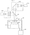
- this sample was subsequently placed on a substrate holder 492 in a surface-modifying device shown in Fig. 2 .
- the substrate holder 492 is set on an XY stage 493 that is two-dimensionally movable under control by a computer (not shown). NO 2 gas was fed from a gas inlet 494, and a vacuum exhaust system 490 was operated so as for the inside pressure to be adjusted to 10 Torr.
- a CO 2 laser 496b (a first light source) for heating and a KrF excimer laser (a second light source) for causing photochemical reaction were controlled by a laser control system (not shown) to effect radiation so synchronized that the both lasers reached a peak power at the same time.
- Infrared light radiated by means of the CO 2 laser 496b was so adjusted by the projection optical system 497b to give the desired spot size (3 ⁇ m in the present example) on the sample 491.
- the infrared light came out from the projection optical system was reflected by a transmission reflecting plate 498, and then shed on the sample 491 through the window 495.
- the transmission reflecting plate is made of a synthetic quartz plate with a thickness of 2 mm. Its transmission reflecting surface is also coated with a high-reflecting film capable of reflecting light with a wavelength of 11.7 to 12.5 ⁇ m and transmitting light (248 nm) radiated from the KrF excimer laser 415.
- the KrF excimer laser 496a As for the light (248 nm) radiated from the second light source, the KrF excimer laser 496a, the light was shed on the sample 491 through the transmission reflecting plate 498 and the window 495 to give the desired spot size (3 ⁇ m in the present example) like the infrared light radiated from the first light source.
- the surface irradiated with the light was heated by the above infrared light to cause a rise of temperature to 350°C, so that the infrared light accelerated the photochemical reaction.
- This surface-modified layer, SiO x film 486 had undergone sufficient oxidation, also having a layer thickness of 70 ⁇ , and thus served as a non-electron-donor.
- this sample 491 was placed on a substrate holder 412 of a CVD apparatus for the selective deposition of Al, shown in Fig. 25, said sample being denoted therein as a sample 411.
- a sample 411 By the following method, Al was deposited only on the surface of an electron donor and no Al was deposited on the non-electron-donor, thus enalbing selective deposition of Al.
- a deposition chamber 417 was evacuated to a pressure of 10 -7 Torr or less by means of a vacuum exhaust system 410. Thereafter, the sample 411 was heated with a heater 413d to 300°C.
- DMAH (CH 3 ) 2 AlH, obtained through a material vaporizing system 415 was supplied from a first gas line of a gas mixer 414, using H 2 as a carrier gas, and H 2 was supplied from a second gas line.
- DMAH and H 2 were fed from a gas inlet 416 into the deposition chamber 417, and the gas mixer 414 and the vacuum exhaust system 410 were operated so as for the total pressure in the deposition chamber 417 to be adjusted to 1.5 Torr and the partial pressure of DHAM to 1.5 x 10 -4 Torr, where the deposition was carried out for 10 minutes.
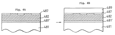
- Figs.4A and 4B an instance in which the surface modification and Al deposition were carried out under the same conditions except that no heating with the CO 2 laser was applied is shown in Figs.4A and 4B .
- the surface-modified layer 487 shown in Fig. 4A was so poor in both the degree of oxidation and the thickness that it could not serve as the non-electron-donor, and hence, Al was deposited over the whole surface as shown by reference numeral 489 in Fig. 4B , and it was impossible to obtain the desired pattern.
- Fig. 5 is a schematic cross section of the apparatus according to the present invention, which, roughly stated, comprises a load lock zone, an optical latent image forming zone and an Al selective deposition zone, which are connected with a gate valve adjoiningly each other.
- reference numeral 701 denotes a substrate which is a sample; 702, a load lock chamber in which the substrate 701 is brought to a vacuum environment or returned to the atmospheric environment; 703a, 703b and 703c, vacuum exhaust systems each comprised of a turbo pump, a rotary pump or the like; 704a, 704b and 704c, gate valves through which the substrate 701 can be put in and out and that can be vacuum-sealed; 705a, 705b and 705c, gas inlets from which gas is fed in; 706b and 706c, substrate holders on which the substrate 701 is placed; 707, a latent image forming chamber in which a latent image layer is formed; 708a, an electron synchrotron or electron storage ring that serves as a light source; 708b, a light control section from which the light with a single or plural wavelength(s) (range) that is necessary among synchrotron orbit radiation light is taken out; 709, an illumination optical system for illuminating
- the substrate 701 whose surface has been cleaned is put in the load lock chamber 702 so that the substrate 701 can be fed in a vacuum environment, and the vacuum exhaust system 703a is operated to evacuated the inside of the load lock chamber 702. Then the gate valve 704b is opened, and the substrate 701 is placed on the substrate holder 706a in the latent image forming chamber 707. With the synchrotron orbit radiation light generated in the light source 708a and controlled by the light control section 708b, the mask 710 used for forming the desired pattern is uniformly irradiated through the window 712 to form a pattern image of the mask 709 by means of the projection optical system 711.
- Materials for the window 712 may vary depending on the wavelength of the light source used, and a window material that does not absorb the light with that wavelength and allows it to pass is selected.
- the vacuum exhaust system 703b is operated to evacuate the inside of the latent image forming chamber 707, and a gas for photochemically changing the surface (e.g., O 2 , O 3 or NO 2 gas when the surface is intended to be oxidized, or N 2 or NH 3 gas when the surface is intended to be nitrided) is fed into the chamber so that only the part irradiated with the light may selectively undergo photochemical reaction (e.g., oxidation, nitriding, reduction) to form on the surface a latent image layer with a thickness of about 50 ⁇ to about 100 ⁇ formed of an oxide film or a nitride film, thereby selectively changing electron donative properties.
- a gas for photochemically changing the surface e.g., O 2 , O 3 or NO 2 gas when the surface is intended to be
- the wavelength of the synchrotron orbit radiation light for causing the photochemical reaction may be selected according to the materials of the substrates and types of gases.
- the substrate 701 is placed on the substrate holder 706c in the Al selective deposition chamber 713 having been evacuated by means of the vacuum exhaust system 703c, and the step of selectively depositing Al or a metal mainly composed of Al is carried out.
- heat CVD is used so that a good-quality Al film or metal film mainly composed of Al can be selectively formed on the substrate 701 as a conductive deposited film.
- an electron donative material is a material in which free electrons are present in the substrate or free electrons are intentionally produced therein, and is exemplified by a material having a surface on which the chemical reaction is accelerated by its exchange with molecules of the starting material gas, adsorbed to the substrate surface.
- a material having a surface on which the chemical reaction is accelerated by its exchange with molecules of the starting material gas, adsorbed to the substrate surface For example, in general, metals or semiconductors are included to this material. It also includes those wherein a thin oxide film is present on the surface of a metal or semiconductor. It can be included therein since the chemical reaction takes place upon exchange of electrons between the substrate and adhered material molecules.
- Such a metal or semiconductor may specifically include semiconductors such as monocrystalline silicon, polycrystalline silicon and amorphous silicon; binary, ternary or quaternary Group III-IV compound semiconductors comprised of any combination of a Group III element Ga, In or Al and a Group IV element P, As or N; and metals, alloys or silicides thereof, such as tungsten, molybdenum, tantalum, tungsten silicide, titanium silicide, aluminum, aluminum silicon, titanium aluminum, titanium nitride, copper, aluminum silicon copper, aluminum palladium, titanium, molybdenum silicide and tantalum silicide.
- semiconductors such as monocrystalline silicon, polycrystalline silicon and amorphous silicon
- binary, ternary or quaternary Group III-IV compound semiconductors comprised of any combination of a Group III element Ga, In or Al and a Group IV element P, As or N
- metals, alloys or silicides thereof such as tungsten, molybdenum, tantalum, tungsten
- Al or the metal mainly composed of Al can be deposited only upon simple thermal reaction in a reaction system comprised of the starting material gas and H 2 .
- a reaction system comprised of DMAH (dimethylaluminum hydride) and H 2 is presumed to basically proceed as follows:
- the DMAH assumes a dimer structure at room temperature.
- MMAH 2 monomethylaluminum hydride
- the above MMAH 2 has a vapor pressure of as low as 0.01 to 0.1 Torr at room temperature and hence it is difficult to transport the starting material in a large quantity, and its rate of deposition is several hundred ⁇ / min at maximum in the present invention. Accordingly, it is most preferred to use DMAH having a vapor pressure of 1 Torr at room temperature.
- the temperature at which the substrate is heated with the heater 714 to deposit Al should be higher than the temperature at which a starting material gas containing Al can be decomposed, and not higher than 450°C. Stated specifically, the substrate temperature should be 160°C to 450°C. When Al is deposited under such conditions, the rate of deposition can be very high, as much as 100 ⁇ /min to 800 ⁇ /min, at a DMAH partial pressure of 10 -4 to 10 -3 Torr, and hence it is possible to attain a sufficiently high deposition rate for an Al deposition technique used for VSLIs. More preferably, the substrate temperature should be 270°C to 350°C.
- Al films deposited under such conditions can be Al films with a good quality, capable of being strongly oriented and also causing no hillocks or spikes in the Al film formed on the Si monocrystalline or Si polycrystalline substrate even when heated at 450°C for 1 hour. Such Al films can also be excellent in electromigration resistance.
- liquid DMAH maintained at room temperature in the gas producing chamber 716 is subjected to bubbling with H 2 or Ar (or other inert gas) serving as a carrier gas to produce the DMAH used for deposition on the substrate.
- H 2 or Ar or other inert gas
- This is transported to the gas mixer 715.
- the H 2 serving as the reactive gas is fed from another route to the gas mixer 715.
- Flow rates of gases are so controlled that each gas has the desired value of partial pressure, and the vacuum exhaust system 703c is operated so as for the total pressure to be kept to a given pressure (10 -3 to 760 Torr).
- the starting material gas and reactive gas are thermally reacted on the heated substrate surface so that the Al or metal mainly composed of Al is selectively deposited on the surface except the non-electron-donative surface formed in the precedent step, in other words, only on the electron-donative surface formed in the precedent step.
- the Al-deposited film thus formed has a resistivity of 2.7 ⁇ cm to 3.0 ⁇ cm at room temperature when its layer thickness is 400 ⁇ , which is substantially equal to the resistivity of an Al bulk, thus giving a continuous and flat film.
- the pressure at the time of film formation can be selected within the range of 10 -3 Torr to 760 Torr.
- the resistivity can also be approximately 2.7 ⁇ cm to 3.0 ⁇ cm at room temperature, and a sufficiently dense film can be formed even with such a layer thickness.
- Reflectance in the visible light wavelength region is substantially 80 %, and a thin film with a good surface flatness can be formed by deposition.
- the film obtained by the metal forming method used in the present invention is dense, has impurities such as carbon in a very small content, has a resistivity comparable to that of a bulk, and also has characteristics with a very high surface smoothness.
- the film can have remarkable effect as stated below.
- Hillocks are projections produced on the Al surface because of partial migration of Al when the release of internal stress occurs during the film formation. A similar phenomenon may also occur when local migration takes place as a result of electrification.
- the Al film formed by the above method has little internal stress and also is nearly in a monocrystalline state.
- conventional Al films may cause hillocks of 10 4 to 10 6 in number/cm 2 as a result of heating at 450°C for 1 hours.
- the hillocks can be greatly reduced to 0 to 10 in number/cm2.
- resist films or interlayer insulating films can be made into thin films. This is advantageous for making films finer and flatter.
- Electromigration is a phenomenon resulting from the migration of wiring atoms caused by the flowing of high-density currents. This phenomenon causes generation and growth of voids along grain boundaries, resulting in a decrease in cross sectional areas, which is accompanied with heat generation and disconnection of wiring .
- the electromigration resistance is commonly evaluated on the basis of average wiring lifetime.
- the wiring formed by a conventional method has an average wiring lifetime of 1 x 10 2 to 10 3 hours (in the case of a wire cross-sectional area of 1 ⁇ m 2 ) under electrification test conditions of 250°C and 1 x 10 6 A/cm 2 .
- the Al film obtained by the metal film forming method used in the present invention has achieved an average wiring lifetime of 10 3 to 10 4 hours in wiring with a cross-sectional area of 1 ⁇ m 2 .
- the wiring can be well suited for practical use if it has a layer thickness of 0.3 ⁇ m in the case of a wiring width of 0.8 ⁇ m. Namely, since the wiring layer thickness can be made small, the irregularities that may be present on the surface of a semiconductor after the wiring has been provided can be prevented to a minimum and also a high reliability can be obtained when usual electric currents are flowed. In addition, a very simple process can be satisfactory for the purpose.
- the optical latent image forming zone is connected with the Al selective deposition zone through the gate valve so that the process can be continuously carried on.
- the same effect can be obtained also when they are independently constructed, though accompanied with a little increase in the number of steps.
- Fig. 6 schematically illustrates the whole of the present apparatus, i.e., a vacuum through-processing apparatus.
- Reference numeral 721 denotes a plasma film forming chamber in which an insulating film and a semiconductor film are formed by plasma deposition, that can be vacuum-sealed; 722, an etching chamber in which films are processed by chemical dry etching, that can be vacuum-sealed; 723, a cleaning chamber in which the surfaces of samples are cleaned using plasma, that can be vacuum-sealed; 724, a transport assembly for transporting the substrate 701 to each processing chamber; and 725, a transport chamber that can be vacuum-sealed, provided with the transport assembly 724.
- Reference numerals 704d, 704e, 704f and 704g each denote a gate valve through which the substrate 701 can be put in and out, that can vacuum-seal each chamber.
- Other components indicated by the same reference numerals as those in Fig. 5 denote the same components.
- an Al electrode pattern is formed on a Si substrate 701 on which an n + a-Si film (n + amorphous silicon film) with a thickness of 2,000 ⁇ has been deposited.
- the gate valve 704a was opened, and the Si substrate 701 was put in the load lock chamber 702.
- the gate valve 704a was closed, and the vacuum exhaust system 703a was operated to evacuate the inside of the load lock chamber 702 to a pressure of 10 -7 Torr or less.
- the vacuum exhaust system 703b was operated to previously evacuate the inside of the latent image forming chamber 707 to a pressure of 10 -8 Torr or less.
- the gate valve 704b was opened and the Si substrate 701 was placed on the substrate holder 706b. O 2 gas was fed from the gas inlet 705b into the latent image forming chamber 707, and the vacuum exhaust system 703b was operated so as for the inside pressure to be adjusted to 20 Torr.
- the light source 708a Using an electron synchrotron as the light source 708a, light with a wavelength of 160 nm to 260 nm was selected in the light control section 708b, with which the mask 710 for forming the electrode pattern was uniformly irradiated by means of the illumination optical system 709. A pattern image of the mask 715 was formed on the surface of the n + a-Si film through the window 712 by means of the projection optical system 711. As a material for the window, quartz was used.
- the gas supply was stopped, and the inside of the latent image forming chamber 707 was evacuated to a pressure of 10 -7 Torr or less.
- the vacuum exhaust system 703c was operated to previously evacuate the inside of the Al selective deposition chamber 713 to a pressure of 10 -7 Torr or less.
- the gate valve 704c was opened and the Si substrate 701 was placed on the substrate holder 706c having been previously heated to 300°C by means of the heater 714 provided inside the Al selective deposition chamber 713.
- the gate valve 704c was closed and the inside of the Al selective deposition chamber 713 was evacuated to a pressure of 10 -8 Torr or less by means of the vacuum exhaust system 703c.
- DMAH was supplied from a first gas line of the gas mixer 715, and H 2 was supplied from a second gas line thereof. After the temperature of the Si substrate 701 reached 300°C, DMAH and H 2 were fed from the gas inlet 705c into the Al selective deposition chamber 713. Then the gas mixer 715 and the vacuum exhaust system 703c were operated so as for the total pressure in the Al selective deposition chamber 713 and the partial pressure of DMAH to be adjusted to 1.5 Torr and 1.5 x 10 -4 Torr, respectively. After deposition was carried out for 10 minutes, the supply of DMAH was stopped, and then the heating with the heater 714 was stopped to cool the Si substrate 701.
- the supply of H 2 was stopped, and the inside of the Al selective deposition chamber 713 was evacuated to a pressure of 10 -7 Torr or less by operating the vacuum exhaust system 703c.
- the gate valves 704c and 704b were opened, and the Si substrate 701 was put in the load lock chamber 702. Then the gate valve 704b was closed, and N 2 gas was fed from the gas inlet 705a until the inside reached the atmospheric pressure. Then the gate valve 704a was opened to take out the Si substrate 701.
- No Al was deposited at all on the surface provided with the latent image, and also was not detectable by surface analysis using Auger electron spectroscopy.
- the gate valve 704a was opened, and a GaAs substrate 701 having been previously cleaned was put in the load lock chamber 702.
- the gate valve 704a was closed, and the vacuum exhaust system 703a was operated to evacuate the inside of the load lock chamber 702 to a pressure of 10 -7 Torr or less.
- the vacuum exhaust system 703b was operated to previously evacuate the inside of the latent image forming chamber 707 to a pressure of 10 -8 Torr or less.
- the gate valve 704b was opened and the GaAs substrate 701 was placed on the substrate holder 706b. NO 2 gas was fed from the gas inlet 705b into the latent image forming chamber 707, and the vacuum exhaust system 703b was operated so as for the inside pressure to be adjusted to 20 Torr.
- the light source 708a Using an electron synchrotron as the light source 708a, light with a wavelength of 300 nm to 600 nm was selected in the light control section 708b, with which the mask 710 for forming the electrode pattern was uniformly irradiated by means of the illumination optical system 709. A pattern image of the mask 715 was formed on the surface of the GaAs substrate 701 through the window 712 by means of the projection optical system 711. As a material for the window, quartz was used. On the surface of the GaAs substrate 701 irradiated with the light, NO 2 and Si caused photochemical reaction only at the part irradiated with the light, and an oxide film with a thickness of about 100 ⁇ was formed on the GaAs substrate 701 surface.
- the gas supply was stopped, and the inside of the latent image forming chamber 707 was evacuated to a pressure of 10 -7 Torr or less.
- the vacuum exhaust system 703c was operated to previously evacuate the inside of the Al selective deposition chamber 713 to a pressure of 10 -7 Torr or less.
- the gate valve 704c was opened and the GaAs substrate 701 was placed on the substrate holder 706c having been previously heated to 300°C by means of the heater 714 provided inside the Al selective deposition chamber 713.
- the gate valve 704c was closed and the inside of the Al selective deposition chamber 713 was evaluated to a pressure of 10 -8 Torr by means of the vacuum exhaust system 703c.
- DMAH was supplied from a first gas line of the gas mixer 715, and H 2 was supplied from a second gas line thereof.
- DMAH and H 2 were fed from the gas inlet 705c into the Al selective deposition chamber 713.
- the gas mixer 715 and the vacuum exhaust system 703c were operated so as for the total pressure in the Al selective deposition chamber 713 and the partial pressure of DMAH to be adjusted to 1.5 Torr and 1.5 x 10 -4 Torr, respectively.
- the supply of DMAH was stopped, and then the heating with the heater 714 was stopped to cool the GaAs substrate 701.
- the supply of H 2 was stopped, and the inside of the Al selective deposition chamber 713 was evacuated to a pressure of 10 -7 Torr or less by operating the vacuum exhaust system 703c.
- the gate valves 704c and 704b were opened, and the GaAs substrate 701 was put in the load lock chamber 702. Then the gate valve 704b was closed, and N 2 gas was fed from the gas inlet 705a until the inside reached the atmospheric pressure. Then the gate valve 704a was opened to take out the GaAs substrate 701. As a result, it was possible to form an Al film with a good quality, like the Al film in Example 2 .
- an amorphous silicon photosensor was fabricated using the vacuum through-processing apparatus shown in Fig. 6 . Its process will be described with reference to Figs. 7A to 7E that show a schematic process chart.
- the gate valve 704a was opened, and a quartz substrate 701 having been previously cleaned was put in the load lock chamber 702.
- the gate valve 704a was closed, and the vacuum exhaust system 703a was operated to evacuate the inside of the load lock chamber 702 to a pressure of 10 -7 Torr or less.
- the inside of the transport chamber 725 was previously evacuated to always keep the pressure to 10 -7 Torr or less by means of a vacuum exhaust system (not shown).
- the gate valve 704g was opened and the sample quartz substrate 701 was taken out of the load lock chamber 702 by means of the transport assembly 724. Then the gate valve 704f was opened, and the substrate 701 was moved through the transport chamber 725 to the cleaning chamber 723 previously evacuated to a pressure of 10 -7 Torr or less by means of the vacuum exhaust system 703f, and placed on the substrate holder 706f. Then the gate valve 704f was closed. The vacuum exhaust system 703f was operated to evacuate the inside of the cleaning chamber 723 to a pressure of 10 -8 Torr or less.
- a gas (in this instance, Ar at a flow rate of 50 sccm) for cleaning the surface of the quartz substrate 701 was led from the gas inlet 705f into the cleaning chamber 723, and an vacuum exhaust system (not shown) was operated so as for the pressure in the cleaning chamber 723 to be adjusted to 0.08 Torr.
- a current with a high frequency of 13.56 MHz and 100W generated in the high-frequency power source was applied to the substrate holder while making adjustment of the matching box, to generate plasma in the space between the substrate holder and the counter electrode. Since the substrate holder was insulated by a capacitor in a direct-current fashion, a negative DC bias voltage of about -60 kV was generated in the substrate holder 706f because of the difference in mobility between electrons and ions.
- the processing time was about 3 minutes. After completion of this processing, the gas supply was stopped, and the inside of the cleaning chamber 723 was evacuated to a pressure of 10 -7 Torr or less.
- the gate valve 704f was opened, and the quartz substrate 701 was taken out by means of the transport assembly 724. Then the gate valve 704f was closed, and the inside of the cleaning chamber 723 was kept evacuated to a pressure of 10 -7 Torr or less.
- the vacuum exhaust system was operated to previously evacuate the inside of the plasma chamber 721 to a pressure of 10 -7 Torr or less.
- the gate valve 704d was opened.
- the quartz substrate 701 was led into the plasma film forming chamber 721, and placed on the substrate holder having been previously heated to 350°C by means of a heater. Then the gate valve 704d was closed.
- the inside of the plasma film forming chamber 721 was evaluated to a pressure of 10 -7 Torr or less by means of the vacuum exhaust system, and the quartz substrate 701 was heated until its temperature reached 350°C.
- SiH 4 , H 2 and NH 3 were fed at flow rates of 10 sccm, 100 sccm and 300 sccm, respectively, into the plasma film forming chamber 721, and the vacuum exhaust system was operated so as for the pressure in the plasma film forming chamber 721 to be adjusted to 0.2 Torr.
- a current with a high frequency of 13.56 MHz and 50 W generated in the high-frequency power source was applied to the counter electrode while making adjustment of the matching box, to generate plasma in the space between the substrate holder and the counter electrode.
- the gases fed in were decomposed with the plasma to deposit an amorphous silicon nitride (a-SiN) film 734 in a thickness of 1,000 ⁇ (Fig. 7A ).
- a-SiN amorphous silicon nitride
- the gas supply was stopped, and the vacuum exhaust system was operated to evacuate the inside of the plasma film forming chamber 721 to a pressure of 10 -7 Torr or less.
- the gate valve 704d was opened, and the quartz substrate 701 was taken out by means of the transport assembly 724.
- the gate valve 704d was closed, and the plasma film forming chamber 721 was evacuated so as for its inside pressure to be kept at 10 -7 Torr or less.
- the latent image forming chamber 707 was previously evacuated to a pressure of 10 -7 Torr or less by means of the vacuum exhaust system 703d.
- the gate valve 704b was opened.
- the quartz substrate 701 was led into the latent image forming chamber 707 by means of the transport assembly 724, and placed on the substrate holder 706b.
- the gate valve 704b was closed.
- the vacuum exhaust system 703b was operated to evacuate the inside of the latent image forming chamber 707 to a pressure of 10 -7 Torr or less.
- a latent image was formed on an a-SiN film 734.
- the gate valve 704b was opened and the quartz substrate 701 was taken out by means of the transport assembly 724.
- the gate valve 704b was closed, and the latent image forming chamber 707 was evacuated so as for its inside pressure to be kept at 10 -7 Torr or less.
- the vacuum exhaust system 703c was operated to previously evacuate the inside of the Al selective deposition chamber 713 to a pressure of 10 -7 Torr or less.
- the gate valve 704c was opened.
- the quartz substrate 701 was led into the Al selective deposition chamber 713 by means of the transport assembly 724 and was placed on the substrate holder 706c.
- the gate valve 704c was closed.
- the vacuum exhaust system 703c was operated to evacuate the inside of the Al selective deposition chamber 713 to a pressure of 10 -8 Torr or less.
- an Al lower electrode 735 with a thickness of 3,000 ⁇ was formed as shown in Fig. 7B .
- the gate valve 704c was opened, and the quartz substrate 701 was taken out by means of the transport assembly 724. Then the gate valve 704c was closed.
- the Al selective deposition chamber 713 was evacuated so as for its inside pressure to be kept at 10 -7 Torr or less.
- the gate valve 704d was opened.
- the quartz substrate 701 was led into the plasma film forming chamber 721 by means of the transport assembly 724, and was placed on the substrate holder previously heated to 350°C with a heater. Then the gate valve 704d was closed.
- the inside of the plasma film forming chamber 721 was evaluated to a pressure of 10 -7 Torr or less by means of the vacuum exhaust system, and the quartz substrate 701 was heated until its temperature reached 350°C.
- SiH 4 , H 2 and NH 3 were fed at flow rates of 10 sccm, 100 sccm and 300 sccm, respectively, from the gas inlet into the plasma film forming chamber 721, and the vacuum exhaust system was operated so as for the pressure in the plasma film forming chamber 721 to be adjusted to 0.2 Torr.
- a current with a high frequency of 13.56 MHz and 50 W generated in the high-frequency power source was applied to the counter electrode while making adjustment of the matching box, to generate plasma in the space between the substrate holder and the counter electrode.
- the gases fed in were decomposed with the plasma to deposit an amorphous silicon nitride (a-SiN) film 736 in a thickness of 3,000 ⁇ as shown in Fig. 7C .
- a-SiN amorphous silicon nitride
- the gas supply was stopped, and the vacuum exhaust system 703d was operated to evacuate the inside of the plasma film forming chamber 721 to a pressure of 10 -7 Torr or less.
- the temperature of the substrate holder 706 was dropped to 250°C to set the temperature of the quartz substrate 701 to 200°C.
- SiH 4 and H 2 were fed at flow rates of 60 sccm and 600 sccm, respectively, into the plasma film forming chamber 721, and the vacuum exhaust system was operated so as for the pressure in the plasma film forming chamber 721 to be adjusted to 0.5 Torr.
- a current with a high frequency of 13.56 MHz and 60 W generated in the high-frequency power source was applied to the counter electrode while making adjustment of the matching box, to generate plasma in the space between the substrate holder and the counter electrode.
- the gases fed in were decomposed with the plasma to deposit an amorphous silicon (a-Si) film 737 in a thickness of 1.5 ⁇ m as shown in Fig. 7C .
- a-Si amorphous silicon
- SiH 4 , H 2 and H 2 -diluted 100 ppm PH 3 were fed at flow rates of 3 sccm, 30 sccm and 400 sccm, respectively, into the plasma film forming chamber 721, and the vacuum exhaust system was operated so as for the pressure in the plasma film forming chamber 721 to be adjusted to 0.5 Torr.
- a current with a high frequency of 13.56 MHz and 300 W generated in the high-frequency power source was applied to the counter electrode while making adjustment of the matching box, to generate plasma in the space between the substrate holder and the counter electrode.
- the gases fed in were decomposed with the plasma to deposit an n + a-Si film 738 in a thickness of 2,000 ⁇ as shown in Fig. 7C .
- the gas supply was stopped, and the vacuum exhaust system was operated to evacuate the inside of the plasma film forming chamber 721 to a pressure of 10 -7 Torr or less.
- the gate valve 704b was opened.
- the quartz substrate 701 was led into the latent image forming chamber 707 by means of the transport assembly 724, and was placed on the substrate holder 706b.
- the gate valve 704b was closed.
- the inside of the latent image forming chamber 707 was evacuated to a pressure of 10 -7 Torr or less by means of the vacuum exhaust system 703b.
- a latent image was formed on the n + a-Si film 738.
- the gate valve 704b was opened and the quartz substrate 701 was taken out by means of the transport assembly 724.
- the gate valve 704b was closed, and the latent image forming chamber 707 was evacuated so as for its inside pressure to be kept at 10 -7 Torr or less.
- the vacuum exhaust system 703c was operated to previously evacuate the inside of the Al selective deposition chamber 713 to a pressure of 10 -7 Torr or less.
- the gate valve 704c was opened.
- the quartz substrate 701 was led into the Al selective deposition chamber 713 by means of the transport assembly 724 and was placed on the substrate holder 706c.
- the gate valve 704c was closed.
- the vacuum exhaust system 703c was operated to evacuate the inside of the Al selective deposition chamber 713 to a pressure of 10 -8 Torr or less.
- an Al upper electrode 739 with a thickness of 6,000 ⁇ was formed as shown in Fig. 7D .
- the gate valve 704c was opened, and the quartz substrate 701 was taken out by means of the transport assembly 724. Then the gate valve 704c was closed.
- the Al selective deposition chamber 713 was evacuated so as for its inside pressure to be kept at 10 -7 Torr or less.
- the vacuum exhaust system was operated to previously evacuate the inside of the etching chamber 722 to a pressure of 10 -7 Torr or less, and the gate valve 704e was opened.
- the quartz substrate 701 was led into the etching chamber 722 by means of the transport assembly 724, and was placed on the substrate holder. Then the gate valve 704e was closed.
- the vacuum exhaust system was operated to evacuated the inside of the etching chamber 722 to a pressure of 10 -7 Torr or less.
- etching gases As etching gases, NF 3 , O 2 and H 2 were fed at flow rates of 700 sccm, 200 sccm and 100 sccm, respectively, from the gas inlet into the microwave plasma gas exciting device, and the vacuum exhaust system was operated so as for the inside of the etching chamber 722 to be adjusted to 0.25 Torr. Microwaves of 2.45 GHz and 700 W generated in a microwave generator were supplied to the microwave plasma gas exciting device, and the etching gas was made to plasma. Only neutral radicals excited by this plasma were transported to the etching chamber 722 through the transport pipe. Using the Al upper electrode 739 as a mask, the latent image of the oxide film formed on the n + a-Si film 738 was first etched.
- NF 3 and O 2 were flowed as etching gases at flow rates of 800 sccm and 200 sccm, respectively, and as shown in Fig. 7D the n + a-Si film 738 was etched to form a light incidence opening 740.
- the etching gas was stopped, and the vacuum exhaust system 703e was operated to evacuate the inside of the etching chamber 722 to a pressure of 10 -7 Torr or less.
- the gate valve 704e was opened, and the quartz substrate 701 was taken out by means of the transport assembly 724.
- the gate valve 704e was closed, and the inside of the etching chamber 722 was evacuated so as to be kept to a pressure of 10 -7 Torr or less.
- the gate valve 704d was opened.
- the quartz substrate 701 was led into the plasma film forming chamber 721 by means of the transport assembly 724, and was placed on the substrate holder previously heated to 350°C with a heater. Then the gate valve 704d was closed.
- the inside of the plasma film forming chamber 721 was evacuated to a pressure of 10 -7 Torr or less by means of the vacuum exhaust system, and the quartz substrate 701 was heated until its temperature reached 350°C.
- SiH 4 , H 2 and NH 3 were fed at flow rates of 10 sccm, 100 sccm and 300 sccm, respectively, from the gas inlet into the plasma film forming chamber 721, and the vacuum exhaust system was operated so as for the pressure in the plasma film forming chamber 721 to be adjusted to 0.2 Torr.
- a current with a high frequency of 13.56 MHz and 80 W generated in the high-frequency power source was applied to the counter electrode while making adjustment of the matching box, to generate plasma in the space between the substrate holder and the counter electrode.
- the gases fed in were decomposed with the plasma to deposit an amorphous silicon nitride (a-SiN) film 741 in a thickness of 2 ⁇ m (Fig. 7E ).
- a-SiN amorphous silicon nitride
- the gas supply was stopped, and the vacuum exhaust system was operated to evacuate the inside of the plasma film forming chamber 721 to a pressure of 10 -7 Torr or less.
- the gate valve 704e was opened, and the quartz substrate 701 was taken out by means of the transport assembly 724.
- the inside of the plasma film forming chamber 721 was evacuated so as for its inside pressure to be kept to 10 -7 Torr or less.
- the gate valve 704g was opened, and the quartz substrate 701 was put in the load lock chamber 702 by means of the transport assembly 724. Then the gate valve 704g was closed. N 2 gas was fed into the load lock chamber 702 so that the pressure in the chamber was returned to the atmospheric pressure, and then the quartz substrate 701 on which the amorphous silicon photosensor had been fabricated was taken out. Measurement of the performance of the amorphous silicon photosensor thus fabricated in the present example revealed that it had a low internal resistance, a high sensitivity and a less dark current.
- the selectively depositing metal is aluminum.
- a metal compound mainly composed of aluminum as exemplified by aluminum silicon that is deposited by reacting DMAH with a silicon-containing gas and hydrogen may also be used as the selectively depositing metal.
- the present invention which is constituted as described above has the following effects.
- the heating of the film to which surface modification is applied in the step of forming the surface-modified layer, accelerates photochemical reaction on the surface irradiated with light, and hence the surface-modified layer can have a chemically stronger bond and also have a larger thickness.
- This can achieve i) an improvement in etching resistance of the surface-modified layer and ii) an increase in difference in electron donative properties between the surface-modified layer and the surface-unmodified layer. This enables pattern formation with ease.
- the optical latent image film is formed using a synchrotron orbit radiation to cause a change in the electron donative properties on the surface, so that the electrode or wiring comprising Al or a metal mainly composed of Al can be selectively formed Since no resist is used, the process can be simplified and the dust is less produced, resulting in an improvement in yield, and metal films with a good quality can be formed. It is also possible to carry out vacuum through-processing of semiconductor devices, without exposure to the atmosphere, and hence semiconductor devices with a high performance can be obtained. Since no Al etching step is required, no after-corrosion occurs, bringing about an improvement in the reliability of devices.
- the present invention can also be effective on the following:
- the substrate can be moved from the latent image forming chamber to the etching chamber through the gate valve. Hence, no dust can be adhered to the substrate surface, and the accuracy in the pattern formation can be improved.
- the latent image forcing chamber is connected with the cleaning chamber similarly through the gate valve, so that the substrate is cleaned before the surface-modified layer is formed on the substrate. This can bring about a great effect.
Landscapes
- Physics & Mathematics (AREA)
- General Physics & Mathematics (AREA)
- Health & Medical Sciences (AREA)
- Chemical & Material Sciences (AREA)
- Engineering & Computer Science (AREA)
- Environmental & Geological Engineering (AREA)
- Public Health (AREA)
- Epidemiology (AREA)
- Chemical Kinetics & Catalysis (AREA)
- Toxicology (AREA)
- Life Sciences & Earth Sciences (AREA)
- Organic Chemistry (AREA)
- General Chemical & Material Sciences (AREA)
- Atmospheric Sciences (AREA)
- Optics & Photonics (AREA)
- Metallurgy (AREA)
- Mechanical Engineering (AREA)
- Materials Engineering (AREA)
- Computer Networks & Wireless Communication (AREA)
- Inorganic Chemistry (AREA)
- Drying Of Semiconductors (AREA)
- Finish Polishing, Edge Sharpening, And Grinding By Specific Grinding Devices (AREA)
- Electrical Discharge Machining, Electrochemical Machining, And Combined Machining (AREA)
- Internal Circuitry In Semiconductor Integrated Circuit Devices (AREA)
- Chemical Vapour Deposition (AREA)
- Electrodes Of Semiconductors (AREA)
Applications Claiming Priority (17)
| Application Number | Priority Date | Filing Date | Title |
|---|---|---|---|
| JP2254196A JP2672185B2 (ja) | 1990-09-26 | 1990-09-26 | 薄膜素子加工方法とその装置 |
| JP254196/90 | 1990-09-26 | ||
| JP255148/90 | 1990-09-27 | ||
| JP2255148A JP2622188B2 (ja) | 1990-09-27 | 1990-09-27 | 薄膜デバイスの微細加工方法 |
| JP261670/90 | 1990-09-29 | ||
| JP2261670A JP2840419B2 (ja) | 1990-09-29 | 1990-09-29 | 光処理法及び光処理装置 |
| JP26646190A JPH04144135A (ja) | 1990-10-05 | 1990-10-05 | 半導体装置の製造法および装置 |
| JP266461/90 | 1990-10-05 | ||
| JP314953/90 | 1990-11-19 | ||
| JP2314953A JP2667930B2 (ja) | 1990-11-19 | 1990-11-19 | 微細加工方法及び装置 |
| JP2313589A JP2709188B2 (ja) | 1990-11-19 | 1990-11-19 | 半導体デバイスの微細加工方法およびその装置 |
| JP314951/90 | 1990-11-19 | ||
| JP2314954A JP2756364B2 (ja) | 1990-11-19 | 1990-11-19 | 光表面処理方法及び処理装置 |
| JP314954/90 | 1990-11-19 | ||
| JP313589/90 | 1990-11-19 | ||
| JP2314951A JP2670465B2 (ja) | 1990-11-19 | 1990-11-19 | 微細加工方法 |
| EP91116309A EP0477890B1 (fr) | 1990-09-26 | 1991-09-25 | Méthode de traitement et appareillage photolithographique |
Related Parent Applications (1)
| Application Number | Title | Priority Date | Filing Date |
|---|---|---|---|
| EP91116309A Division EP0477890B1 (fr) | 1990-09-26 | 1991-09-25 | Méthode de traitement et appareillage photolithographique |
Publications (1)
| Publication Number | Publication Date |
|---|---|
| EP0909985A1 true EP0909985A1 (fr) | 1999-04-21 |
Family
ID=27573548
Family Applications (8)
| Application Number | Title | Priority Date | Filing Date |
|---|---|---|---|
| EP98124751A Withdrawn EP0908781A3 (fr) | 1990-09-26 | 1991-09-25 | Méthode de traitement et appareillage photolithographique |
| EP98124748A Withdrawn EP0909986A1 (fr) | 1990-09-26 | 1991-09-25 | Méthode de traitement et appareillage photolithographique |
| EP98124749A Withdrawn EP0909987A1 (fr) | 1990-09-26 | 1991-09-25 | Méthode de traitement et appareillage photolithographique |
| EP98124755A Withdrawn EP0909989A1 (fr) | 1990-09-26 | 1991-09-25 | Méthode de traitement et appareillage photolithographique |
| EP98124753A Withdrawn EP0909988A1 (fr) | 1990-09-26 | 1991-09-25 | Méthode de traitement photolithographique |
| EP98124750A Withdrawn EP0909985A1 (fr) | 1990-09-26 | 1991-09-25 | Méthode de traitement et appareillage photolithographique |
| EP91116309A Expired - Lifetime EP0477890B1 (fr) | 1990-09-26 | 1991-09-25 | Méthode de traitement et appareillage photolithographique |
| EP98124754A Withdrawn EP0908782A1 (fr) | 1990-09-26 | 1991-09-25 | Méthode de traitement photolithographique |
Family Applications Before (5)
| Application Number | Title | Priority Date | Filing Date |
|---|---|---|---|
| EP98124751A Withdrawn EP0908781A3 (fr) | 1990-09-26 | 1991-09-25 | Méthode de traitement et appareillage photolithographique |
| EP98124748A Withdrawn EP0909986A1 (fr) | 1990-09-26 | 1991-09-25 | Méthode de traitement et appareillage photolithographique |
| EP98124749A Withdrawn EP0909987A1 (fr) | 1990-09-26 | 1991-09-25 | Méthode de traitement et appareillage photolithographique |
| EP98124755A Withdrawn EP0909989A1 (fr) | 1990-09-26 | 1991-09-25 | Méthode de traitement et appareillage photolithographique |
| EP98124753A Withdrawn EP0909988A1 (fr) | 1990-09-26 | 1991-09-25 | Méthode de traitement photolithographique |
Family Applications After (2)
| Application Number | Title | Priority Date | Filing Date |
|---|---|---|---|
| EP91116309A Expired - Lifetime EP0477890B1 (fr) | 1990-09-26 | 1991-09-25 | Méthode de traitement et appareillage photolithographique |
| EP98124754A Withdrawn EP0908782A1 (fr) | 1990-09-26 | 1991-09-25 | Méthode de traitement photolithographique |
Country Status (4)
| Country | Link |
|---|---|
| US (4) | US5962194A (fr) |
| EP (8) | EP0908781A3 (fr) |
| AT (1) | ATE200829T1 (fr) |
| DE (1) | DE69132587T2 (fr) |
Families Citing this family (40)
| Publication number | Priority date | Publication date | Assignee | Title |
|---|---|---|---|---|
| IL119246A (en) * | 1996-09-12 | 2000-10-31 | Oramir Semiconductor Ltd | Laser removal of foreign materials from surfaces |
| US6107206A (en) * | 1998-09-14 | 2000-08-22 | Taiwan Semiconductor Manufacturing Company | Method for etching shallow trenches in a semiconductor body |
| US6727980B2 (en) | 1998-09-17 | 2004-04-27 | Nikon Corporation | Apparatus and method for pattern exposure and method for adjusting the apparatus |
| US6192897B1 (en) * | 1999-01-27 | 2001-02-27 | Euv Llc | Apparatus and method for in-situ cleaning of resist outgassing windows |
| US6762412B1 (en) * | 1999-05-10 | 2004-07-13 | Nikon Corporation | Optical apparatus, exposure apparatus using the same, and gas introduction method |
| CN1315822A (zh) * | 2000-03-30 | 2001-10-03 | 日本胜利株式会社 | 印刷电路板的薄膜电阻体元件及其形成方法 |
| JP4286439B2 (ja) * | 2000-08-11 | 2009-07-01 | 富士通マイクロエレクトロニクス株式会社 | 半導体装置の製造方法 |
| KR100408137B1 (ko) * | 2001-11-26 | 2003-12-06 | 학교법인 성균관대학 | 중성빔을 이용한 층대층 식각장치 및 식각방법 |
| US6781126B2 (en) * | 2002-02-04 | 2004-08-24 | Applied Materials, Inc. | Auger-based thin film metrology |
| US20040007733A1 (en) * | 2002-06-26 | 2004-01-15 | Macronix International Co., Ltd. | Floating gate memory cell and forming method |
| KR100585472B1 (ko) * | 2002-09-30 | 2006-06-07 | 에이에스엠엘 네델란즈 비.브이. | 리소그래피장치 및 디바이스 제조방법 |
| EP1403715A3 (fr) * | 2002-09-30 | 2006-01-18 | ASML Netherlands B.V. | Appareil lithographique et méthode pour la fabrication d'un dispositif |
| US7022615B2 (en) * | 2002-11-26 | 2006-04-04 | Matsushita Electric Industrial Co., Ltd. | Plasma processing method |
| JP2004221545A (ja) * | 2002-12-26 | 2004-08-05 | Tokyo Electron Ltd | プラズマエッチング方法 |
| WO2004079450A1 (fr) * | 2003-03-06 | 2004-09-16 | Yissum Research Development Company Of The Hebrew University Of Jerusalem | Procede de production d'une structure a motifs |
| US6872972B2 (en) * | 2003-07-16 | 2005-03-29 | Macronix International Co., Ltd. | Method for forming silicon film with changing grain size by thermal process |
| JP3655915B2 (ja) * | 2003-09-08 | 2005-06-02 | Fcm株式会社 | 導電性シートおよびそれを含む製品 |
| WO2005019493A2 (fr) * | 2003-08-11 | 2005-03-03 | Honeywell International Inc. | Constructions de plaque cible et de contreplaque et procede de fabrication de ces constructions de plaque cible et de contreplaque |
| US20050221586A1 (en) * | 2003-12-18 | 2005-10-06 | Mulligan Rose A | Methods and apparatus for laser dicing |
| JP5102492B2 (ja) * | 2003-12-19 | 2012-12-19 | カール・ツァイス・エスエムティー・ゲーエムベーハー | 結晶素子を有するマイクロリソグラフィー投影用対物レンズ |
| US7151883B2 (en) * | 2004-10-08 | 2006-12-19 | Hewlett-Packard Development Company, L.P. | Photonic crystal device and methods |
| JP5080009B2 (ja) | 2005-03-22 | 2012-11-21 | 日立ビアメカニクス株式会社 | 露光方法 |
| JP4599342B2 (ja) * | 2005-12-27 | 2010-12-15 | エーエスエムエル ネザーランズ ビー.ブイ. | 光学装置、リソグラフィ装置、および、デバイス製造方法 |
| US20090227093A1 (en) * | 2006-02-17 | 2009-09-10 | Cornell Research Foundation, Inc | Patterning During Film Growth |
| US7449414B2 (en) * | 2006-08-07 | 2008-11-11 | Tokyo Electron Limited | Method of treating a mask layer prior to performing an etching process |
| US20080073596A1 (en) * | 2006-08-24 | 2008-03-27 | Asml Netherlands B.V. | Lithographic apparatus and method |
| JP2008251913A (ja) * | 2007-03-30 | 2008-10-16 | Hoya Candeo Optronics株式会社 | 耐紫外線材料、ならびにこれを用いたシール部材、緩衝部材、遮光部材、光源装置、及び処理装置 |
| JP4969304B2 (ja) * | 2007-04-20 | 2012-07-04 | 東京エレクトロン株式会社 | 熱処理板の温度設定方法、熱処理板の温度設定装置及びコンピュータ読み取り可能な記憶媒体 |
| US8013300B2 (en) * | 2008-06-20 | 2011-09-06 | Carl Zeiss Nts, Llc | Sample decontamination |
| EP2144117A1 (fr) * | 2008-07-11 | 2010-01-13 | The Provost, Fellows and Scholars of the College of the Holy and Undivided Trinity of Queen Elizabeth near Dublin | Procédé et système de fabrication de motifs sur une surface |
| US8536056B2 (en) * | 2011-08-22 | 2013-09-17 | Nanya Technology Corporation | Method of forming conductive pattern |
| WO2016099755A1 (fr) * | 2014-12-15 | 2016-06-23 | Applied Materials, Inc. | Barrière de diffusion diélectrique ultra mince et couche d'arrêt de gravure pour des applications d'interconnexion de pointe |
| CN104505334B (zh) * | 2014-12-16 | 2017-10-24 | 桂林电子科技大学 | 一种通过激光加热制作薄膜图案的方法 |
| US9613808B1 (en) * | 2016-01-19 | 2017-04-04 | United Microelectronics Corp. | Method of forming multilayer hard mask with treatment for removing impurities and forming dangling bonds |
| US10872760B2 (en) * | 2016-07-26 | 2020-12-22 | Taiwan Semiconductor Manufacturing Co., Ltd. | Cluster tool and manufacuturing method of semiconductor structure using the same |
| CN107799407B (zh) * | 2016-08-29 | 2020-07-17 | 中国科学院苏州纳米技术与纳米仿生研究所 | 一种晶体管的凹槽栅制备方法及大功率射频器件 |
| JP6500874B2 (ja) * | 2016-10-21 | 2019-04-17 | 株式会社豊田中央研究所 | 半導体基板の光電気化学エッチングに用いるエッチング装置 |
| EP3606293B1 (fr) * | 2017-03-31 | 2022-09-07 | Fuji Corporation | Dispositif de génération de plasma |
| CN108735584B (zh) * | 2018-05-29 | 2021-03-23 | 江苏永鼎股份有限公司 | 一种半导体芯片生产工艺 |
| EP3875633A1 (fr) * | 2020-03-03 | 2021-09-08 | Stichting Nederlandse Wetenschappelijk Onderzoek Instituten | Procédé et appareil de formation d'une couche de matériau à motifs |
Citations (3)
| Publication number | Priority date | Publication date | Assignee | Title |
|---|---|---|---|---|
| WO1989011553A1 (fr) * | 1988-05-23 | 1989-11-30 | Hughes Aircraft Company | Procede de tirage et de nucleation par regions selectives servant a la deposition en phase gazeuse de metal par procede chimique au moyen de faisceaux ioniques focalises |
| EP0429070A2 (fr) * | 1989-11-21 | 1991-05-29 | Max-Planck-Gesellschaft zur Förderung der Wissenschaften e.V. | Traitement d'une surface destinée à être métallisée à l'aide de radiations émises par un synchrotron |
| EP0456479A2 (fr) * | 1990-05-09 | 1991-11-13 | Canon Kabushiki Kaisha | Procédé et appareil de formation de motifs et procédé de fabrication de dispositifs semi-conducteurs utilisant de tels motifs |
Family Cites Families (35)
| Publication number | Priority date | Publication date | Assignee | Title |
|---|---|---|---|---|
| US3326717A (en) * | 1962-12-10 | 1967-06-20 | Ibm | Circuit fabrication |
| US4845529A (en) * | 1987-12-18 | 1989-07-04 | Thomas W. Secrest | Storage apparatus comprising a plurality of layers |
| US4324854A (en) * | 1980-03-03 | 1982-04-13 | California Institute Of Technology | Deposition of metal films and clusters by reactions of compounds with low energy electrons on surfaces |
| JPS56164523A (en) * | 1980-05-21 | 1981-12-17 | Hitachi Ltd | Vapor phase growth of semiconductor |
| US4579750A (en) * | 1980-07-07 | 1986-04-01 | Massachusetts Institute Of Technology | Laser heated CVD process |
| US4361461A (en) * | 1981-03-13 | 1982-11-30 | Bell Telephone Laboratories, Incorporated | Hydrogen etching of semiconductors and oxides |
| JPS57208142A (en) * | 1981-06-17 | 1982-12-21 | Toshiba Corp | Method for forming fine pattern |
| JPS5839779A (ja) * | 1981-09-01 | 1983-03-08 | Matsushita Electric Ind Co Ltd | 写真蝕刻方法 |
| JPS59161038A (ja) * | 1983-03-04 | 1984-09-11 | Hitachi Ltd | パタ−ン形成法 |
| JPS59194440A (ja) * | 1983-04-18 | 1984-11-05 | Mitsubishi Electric Corp | パタ−ン形成装置 |
| FR2548218B1 (fr) * | 1983-06-29 | 1987-03-06 | Pauleau Yves | Procede de depot de couches minces par reaction chimique en phase gazeuse utilisant deux rayonnements differents |
| US4470871A (en) * | 1983-12-27 | 1984-09-11 | Rca Corporation | Preparation of organic layers for oxygen etching |
| JPH07107190B2 (ja) * | 1984-03-30 | 1995-11-15 | キヤノン株式会社 | 光化学気相成長方法 |
| JPS60211074A (ja) * | 1984-04-05 | 1985-10-23 | Fuji Electric Corp Res & Dev Ltd | 導電膜パタ−ンの形成方法 |
| JPS6129129A (ja) * | 1984-07-19 | 1986-02-10 | Toshiba Corp | ドライエツチング方法 |
| JPS6167228A (ja) * | 1984-09-10 | 1986-04-07 | Hitachi Ltd | 微細パタ−ン形成法 |
| JPS61104614A (ja) * | 1984-10-29 | 1986-05-22 | Canon Inc | 堆積膜形成法 |
| US4810601A (en) * | 1984-12-07 | 1989-03-07 | International Business Machines Corporation | Top imaged resists |
| JPS61187237A (ja) * | 1985-02-14 | 1986-08-20 | Toshiba Corp | パタ−ン形成方法 |
| US4685976A (en) * | 1985-04-10 | 1987-08-11 | Eaton Corporation | Multi-layer semiconductor processing with scavenging between layers by excimer laser |
| US4612085A (en) * | 1985-04-10 | 1986-09-16 | Texas Instruments Incorporated | Photochemical patterning |
| US4670063A (en) * | 1985-04-10 | 1987-06-02 | Eaton Corporation | Semiconductor processing technique with differentially fluxed radiation at incremental thicknesses |
| US4619894A (en) * | 1985-04-12 | 1986-10-28 | Massachusetts Institute Of Technology | Solid-transformation thermal resist |
| JPH0770513B2 (ja) * | 1985-05-13 | 1995-07-31 | 株式会社日立製作所 | エッチングの方法およびエッチング装置 |
| JPS61278146A (ja) * | 1985-06-03 | 1986-12-09 | Toshiba Corp | 光処理方法 |
| US4931380A (en) * | 1985-07-18 | 1990-06-05 | Microsi, Inc. | Pre-exposure method for increased sensitivity in high contrast resist development of positive working diazo ketone photoresist |
| JPS62262433A (ja) * | 1986-05-09 | 1987-11-14 | Hitachi Ltd | 表面処理方法 |
| JP2559030B2 (ja) * | 1986-07-25 | 1996-11-27 | 日本電信電話株式会社 | 金属薄膜の製造方法 |
| JPH0774452B2 (ja) * | 1986-11-27 | 1995-08-09 | キヤノン株式会社 | 光化学気相成長法による機能性堆積膜の形成方法 |
| JPS63165845A (ja) * | 1986-12-26 | 1988-07-09 | Toshiba Corp | パタ−ン形成方法 |
| US5062149A (en) * | 1987-10-23 | 1991-10-29 | General Dynamics Corporation | Millimeter wave device and method of making |
| US5041361A (en) * | 1988-08-08 | 1991-08-20 | Midwest Research Institute | Oxygen ion-beam microlithography |
| JPH02265240A (ja) * | 1989-04-06 | 1990-10-30 | Matsushita Electron Corp | ドライエッチング装置 |
| US5106764A (en) * | 1989-04-10 | 1992-04-21 | At&T Bell Laboratories | Device fabrication |
| US5503961A (en) * | 1994-11-02 | 1996-04-02 | International Business Machines Corporation | Process for forming multilayer lift-off structures |
-
1991
- 1991-09-25 EP EP98124751A patent/EP0908781A3/fr not_active Withdrawn
- 1991-09-25 EP EP98124748A patent/EP0909986A1/fr not_active Withdrawn
- 1991-09-25 EP EP98124749A patent/EP0909987A1/fr not_active Withdrawn
- 1991-09-25 DE DE69132587T patent/DE69132587T2/de not_active Expired - Fee Related
- 1991-09-25 AT AT91116309T patent/ATE200829T1/de not_active IP Right Cessation
- 1991-09-25 EP EP98124755A patent/EP0909989A1/fr not_active Withdrawn
- 1991-09-25 EP EP98124753A patent/EP0909988A1/fr not_active Withdrawn
- 1991-09-25 EP EP98124750A patent/EP0909985A1/fr not_active Withdrawn
- 1991-09-25 EP EP91116309A patent/EP0477890B1/fr not_active Expired - Lifetime
- 1991-09-25 EP EP98124754A patent/EP0908782A1/fr not_active Withdrawn
-
1994
- 1994-05-31 US US08/251,666 patent/US5962194A/en not_active Expired - Fee Related
-
1995
- 1995-04-25 US US08/429,287 patent/US5863706A/en not_active Expired - Fee Related
- 1995-04-25 US US08/429,288 patent/US6025115A/en not_active Expired - Fee Related
- 1995-04-25 US US08/429,289 patent/US5981001A/en not_active Expired - Fee Related
Patent Citations (3)
| Publication number | Priority date | Publication date | Assignee | Title |
|---|---|---|---|---|
| WO1989011553A1 (fr) * | 1988-05-23 | 1989-11-30 | Hughes Aircraft Company | Procede de tirage et de nucleation par regions selectives servant a la deposition en phase gazeuse de metal par procede chimique au moyen de faisceaux ioniques focalises |
| EP0429070A2 (fr) * | 1989-11-21 | 1991-05-29 | Max-Planck-Gesellschaft zur Förderung der Wissenschaften e.V. | Traitement d'une surface destinée à être métallisée à l'aide de radiations émises par un synchrotron |
| EP0456479A2 (fr) * | 1990-05-09 | 1991-11-13 | Canon Kabushiki Kaisha | Procédé et appareil de formation de motifs et procédé de fabrication de dispositifs semi-conducteurs utilisant de tels motifs |
Non-Patent Citations (2)
| Title |
|---|
| MASU K ET AL: "ALUMINUM DEPOSITION FROM WEEKLY-EXCITED METALORGANIC SOURCE BY HYBRID-EXCITATION CVD", EXTENDED ABSTRACTS OF THE INTERNATIONAL CONFERENCE ON SOLID STATE DEVICES AND MATERIALS, TOKYO, AUG. 24 - 26, 1988, no. CONF. 20, 24 August 1988 (1988-08-24), JAPAN SOCIETY OF APPLIED PHYSICS, XP000041548 * |
| URISU T ET AL: "SYNCHROTRON RADIATION STIMULATED SEMICONDUCTOR PROCESSES: CHEMICAL VAPOR DEPOSITION AND ETCHING", REVIEW OF SCIENTIFIC INSTRUMENTS, vol. 60, no. 7, PART 2B, July 1989 (1989-07-01), pages - 2, XP000038319 * |
Also Published As
| Publication number | Publication date |
|---|---|
| US5981001A (en) | 1999-11-09 |
| DE69132587D1 (de) | 2001-05-31 |
| EP0908781A3 (fr) | 1999-04-21 |
| ATE200829T1 (de) | 2001-05-15 |
| US6025115A (en) | 2000-02-15 |
| US5962194A (en) | 1999-10-05 |
| EP0909987A1 (fr) | 1999-04-21 |
| EP0908782A1 (fr) | 1999-04-14 |
| EP0477890A3 (en) | 1996-12-18 |
| EP0477890A2 (fr) | 1992-04-01 |
| EP0909988A1 (fr) | 1999-04-21 |
| EP0908781A2 (fr) | 1999-04-14 |
| EP0909989A1 (fr) | 1999-04-21 |
| EP0477890B1 (fr) | 2001-04-25 |
| US5863706A (en) | 1999-01-26 |
| DE69132587T2 (de) | 2001-09-06 |
| EP0909986A1 (fr) | 1999-04-21 |
Similar Documents
| Publication | Publication Date | Title |
|---|---|---|
| EP0909985A1 (fr) | Méthode de traitement et appareillage photolithographique | |
| US5508066A (en) | Method for forming a thin film | |
| EP0425084B1 (fr) | Procédé de déposition d'un film utilisant un hydride d'aluminium alkylé | |
| JP3048749B2 (ja) | 薄膜形成方法 | |
| EP0420595A2 (fr) | Formation d'un film déposé sélectivement utilisant de l'hydrure d'alkyl-aluminium double de métal | |
| EP0448223A2 (fr) | Procédé de formation d'un film de métal déposé avec de l'aluminium comme composant principal utilisant d'hydrure d'alkyl aluminium | |
| US5714306A (en) | Processing method and apparatus | |
| JP2726118B2 (ja) | 堆積膜形成法 | |
| EP0288754B1 (fr) | Procédé CVD à haut rendement pour le dépôt de tungstène sous forme de films sans tension | |
| EP0498580A1 (fr) | Méthode dépôt d'un film métallique contenant de l'aluminium en utilisant un halide d'alkylaluminium | |
| JPS61127121A (ja) | 薄膜形成方法 | |
| EP0539948B1 (fr) | Appareillage et procédé pour fabriquer des films métalliques | |
| EP0420597A2 (fr) | Procédé pour la formation d'un film déposé en utilisant de l'alkyle de l'hydrure d'aluminium et procédé de fabrication d'un dispositif semi-conducteur | |
| US6303499B1 (en) | Process for preparing semiconductor device | |
| JPS6248752B2 (fr) | ||
| JPH03110842A (ja) | 堆積膜形成法 | |
| JP2831770B2 (ja) | 堆積膜形成法 | |
| JP2721020B2 (ja) | 堆積膜形成法 | |
| JP2721021B2 (ja) | 堆積膜形成法 | |
| JP3395348B2 (ja) | 反射防止膜の形成方法 | |
| JPH03110838A (ja) | 堆積膜形成法 | |
| JPH04144135A (ja) | 半導体装置の製造法および装置 | |
| JP2945886B2 (ja) | 半導体集積回路装置用配線構造の製造法 | |
| JPH08325082A (ja) | 堆積膜形成法 | |
| JPH03110841A (ja) | 堆積膜形成法 |
Legal Events
| Date | Code | Title | Description |
|---|---|---|---|
| PUAI | Public reference made under article 153(3) epc to a published international application that has entered the european phase |
Free format text: ORIGINAL CODE: 0009012 |
|
| AC | Divisional application: reference to earlier application |
Ref document number: 477890 Country of ref document: EP |
|
| AK | Designated contracting states |
Kind code of ref document: A1 Designated state(s): AT BE CH DE DK ES FR GB GR IT LI LU NL SE |
|
| 17P | Request for examination filed |
Effective date: 19990914 |
|
| 17Q | First examination report despatched |
Effective date: 20000317 |
|
| STAA | Information on the status of an ep patent application or granted ep patent |
Free format text: STATUS: THE APPLICATION IS DEEMED TO BE WITHDRAWN |
|
| 18D | Application deemed to be withdrawn |
Effective date: 20000928 |