EP0905765B1 - Endpunktfühlung und Apparat - Google Patents
Endpunktfühlung und Apparat Download PDFInfo
- Publication number
- EP0905765B1 EP0905765B1 EP98116749A EP98116749A EP0905765B1 EP 0905765 B1 EP0905765 B1 EP 0905765B1 EP 98116749 A EP98116749 A EP 98116749A EP 98116749 A EP98116749 A EP 98116749A EP 0905765 B1 EP0905765 B1 EP 0905765B1
- Authority
- EP
- European Patent Office
- Prior art keywords
- fuse structure
- oxide layer
- layer
- recited
- terminal via
- Prior art date
- Legal status (The legal status is an assumption and is not a legal conclusion. Google has not performed a legal analysis and makes no representation as to the accuracy of the status listed.)
- Expired - Lifetime
Links
Images


Classifications
-
- H—ELECTRICITY
- H01—ELECTRIC ELEMENTS
- H01J—ELECTRIC DISCHARGE TUBES OR DISCHARGE LAMPS
- H01J37/00—Discharge tubes with provision for introducing objects or material to be exposed to the discharge, e.g. for the purpose of examination or processing thereof
- H01J37/32—Gas-filled discharge tubes
- H01J37/32917—Plasma diagnostics
- H01J37/32935—Monitoring and controlling tubes by information coming from the object and/or discharge
- H01J37/32963—End-point detection
-
- H—ELECTRICITY
- H10—SEMICONDUCTOR DEVICES; ELECTRIC SOLID-STATE DEVICES NOT OTHERWISE PROVIDED FOR
- H10W—GENERIC PACKAGES, INTERCONNECTIONS, CONNECTORS OR OTHER CONSTRUCTIONAL DETAILS OF DEVICES COVERED BY CLASS H10
- H10W20/00—Interconnections in chips, wafers or substrates
- H10W20/01—Manufacture or treatment
- H10W20/031—Manufacture or treatment of conductive parts of the interconnections
-
- H—ELECTRICITY
- H10—SEMICONDUCTOR DEVICES; ELECTRIC SOLID-STATE DEVICES NOT OTHERWISE PROVIDED FOR
- H10W—GENERIC PACKAGES, INTERCONNECTIONS, CONNECTORS OR OTHER CONSTRUCTIONAL DETAILS OF DEVICES COVERED BY CLASS H10
- H10W20/00—Interconnections in chips, wafers or substrates
- H10W20/40—Interconnections external to wafers or substrates, e.g. back-end-of-line [BEOL] metallisations or vias connecting to gate electrodes
- H10W20/49—Adaptable interconnections, e.g. fuses or antifuses
- H10W20/493—Fuses, i.e. interconnections changeable from conductive to non-conductive
Definitions
- the present relates to the design and manufacture of semiconductor devices. More particularly, the present invention relates to improved techniques for detecting etch endpoints in metal fuse fabrication.
- Metal fuses are typically patterned from existing metallization layers that are fabricated over dielectric layers of a silicon wafer. By way of example, after a metallization layer is deposited over a dielectric layer, a spin-coating process is used to apply a photoresist over the metallization layer.
- the photoresist layer is then patterned with a reticle-stepper apparatus, which is used to transfer a desired pattern to the photoresist layer. Once patterned ( i.e ., exposed and developed), the photoresist will resemble a mask that leaves exposed certain regions of the underlying metallization, while still covering other portions of the metallization layer. Next, an etching operations is performed to remove portions of the metallization layer where the photoresist was not present. At this point, the metallization layer will have been patterned to define any number of features, such as interconnection lines and metal fuse structures. The metallization layer may then be covered with a dielectric layer, and terminal via (TV) holes etched down close to the metal fuse structures. However, in metal fuse technology, there is a general requirement that a certain thickness of dielectric layer remain over the metal fuse structure to ensure appropriate functionality.
- TV terminal via
- a common problem in etching the terminal vias is that the amount of dielectric material overlying the metal fuse structures varies in thickness depends on the type of deposition technique used, the location of neighboring features and the region of the wafer being patterned. As a result, the timed etching processes have to be varied to take into account these and other factors. Unfortunately, such variations in the formation of the terminal vias may translate into substantial losses in productivity as well as damaged metal fuse structures. That is, if the terminal via etching operation removes too much of the overlying dielectric, or etches down into the metallization layer, the metal fuse structure may become too damaged to work for its intended purpose.
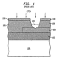
- Figure 1 shows a cross-sectional view of a semiconductor wafer 100 having a number of layers fabricated thereon.
- a dielectric layer 102 is commonly deposited over the semiconductor wafer 100 to a thickness that sufficiently insulates any active devices patterned throughout the semiconductor wafer 100.
- a metallization layer is formed over the dielectric layer 102 and parterned in the aforementioned method to form a metallization feature 104.
- the metallization feature 104 is fabricated in the form of a metal fuse structure that may be programmed to store bit data or interconnect devices.
- an oxide layer 106 is deposited over the metallization feature 104, as well as over other features throughout the semiconductor wafer.
- an amount of oxide e.g. , to a level 120 remain over the metallization feature 104 to enable appropriate programming.
- the level 120 of oxide that remains should range between about 1,000 angstroms and 3,000 angstroms.
- EP 0 762 498 A2 relates to a fuse window structure and a method for forming the same for a semiconductor device.
- Different fuse window structures are formed by using etched stops with different configurations.
- this invention does not involve the detection of the level of a dopant species that is emitted when the doped oxide layer begins to etch, and there upon termination of the etching.
- the present invention fills these needs by providing a method and apparatus that improves the process of forming terminal vias over metal fuse structures in devices having varying oxide thicknesses.
- a method for detecting an etch end-point during the formation of terminal vias; while simultaneously improving stress migration problems is disclosed.
- a method of forming a terminal via in a fuse structure includes forming the fuse structure from a metallization layer. Depositing a bottom oxide layer that is an HDP oxide over the fuse structure that is formed from the metallization layer. Depositing a doped oxide layer over the base oxide layer. Depositing a top oxide layer over the doped oxide layer. Etching through the top oxide layer. Detecting an increased level of a dopant species that is emitted when the doped oxide layer begins to etch. The method further includes terminating the etching when the increased level of dopant species is detected. Wherein at least the bottom oxide layer remains over the fuse structure that is formed from the metallization layer.
- a metal fuse structure in another embodiment, includes a fuse structure that is patterned from a metallization layer. A base oxide layer lying over the fuse structure, the base oxide layer having a thickness of between about 500 angstroms and about 2,000 angstroms. An etch stop signal layer lying over the base oxide layer. A top oxide layer lying over the etch stop signal layer The structure further includes a terminal via that is defined through the top oxide layer that lies over the fuse structure. Wherein the terminal via is not defined past the etch stop layer, and the base oxide layer lying over the fuse structure remains.
- a metal fuse structure in ye: another embodiment, is disclosed.
- the structure includes a fuse structure that is patterned from a metallization layer.
- a base oxide layer lies over the fuse structure, and the base oxide layer has a thickness of between about 500 angstroms and about 2,000 angstroms.
- a spin-on-glass etch stop layer lies over the base oxide layer.
- a top oxide layer lies over the spin-on-glass etch stop layer.
- the structure further includes a terminal via that is defined through the top oxide layer that lies over the fuse structure, such that the terminal via is not defined past the spin-on-glass etch stop layer, and the base oxide layer lying over the fuse structure remains.
- the metal fuse structures when metal fuse structures maintain a sufficient amount of oxide over the terminal vias, the metal fuse structures will operate substantially better in a number of applications, which may include cell replacement in DRAM devices, programming bit data or micro-code onto a chip, etc. Therefore, the combined ability to maintain a desired amount of oxide over a terminal via (regardless of variations in oxide) and the introduction of less compressive materials in the intermetal dielectric layers will improve fuse performance and reduce stress migration in underlying metallization features.
- Other aspects and advantages of the invention will become apparent from the following detailed description, taken in conjunction with the accompanying drawings, illustrating by way of example the principles of the invention.
- the invention relates to the formation of terminal vias for use in integrated circuits (ICs).
- ICs include, for example, random access memories (RAMs), dynamic RAMs (DRAMs), a synchronous DRAM (SDRAM), read only memories (ROMs).
- RAMs random access memories
- DRAMs dynamic RAMs
- SDRAM synchronous DRAM
- ROMs read only memories
- Ics such as application specific ICs (ASICs), merged DRAM-logic circuits (embedded DRAMs), or other logic circuits, are also useful.
- ICs are formed on the wafer in parallel. After processing is finished, the wafer is diced to separate the ICs to individual chips. The chips are then packaged, resulting in a final product that is used in, for example, consumer products such as computer systems, cellular phones, personal digital assistants (PDAs), and other electronic products.
- PDAs personal digital assistants
- an improved process of forming terminal vias over metal fuse structures in devices having varying oxide thicknesses is disclosed.
- a method for detecting when an etch end-point is reached in the formation of terminal vias, while introducing a self-stress relief component into a multi-level intermediate dielectric process is also disclosed.
- Figure 2 shows a cross-sectional view of a semiconductor wafer 200 having a first oxide layer 202 deposited thereon in accordance with one embodiment of the present invention
- the first oxide layer 202 is deposited using a conventional chemical vapor deposition (CVD) method for depositing oxide material to a desired level.
- CVD chemical vapor deposition
- the first oxide layer 202 may be planarized using any number of techniques, including a conventional chemical mechanical polishing (CMP) technique that produces a substantially flat oxide surface.
- CMP chemical mechanical polishing
- a metallization material is blanket deposited over the first oxide layer 202 using any number of conventional metal deposition techniques, such as sputtering or the like.
- the metallization material is then patterned using a photoresist mask (not shown), that enables the formation of features 204a and 204b on the metallization layer 204.
- FIG 3 shows a cross-sectional view of Figure 2 after a high density plasma (HDP) oxide layer 302 is deposited over the first oxide layer 202 and the metallization layer 204.
- HDP oxide is one of the best gap filling processes used for intermetal dielectric applications.
- the HDP oxide 302 is deposited to a thickness of between about 500 angstroms and about 5,000 angstroms, and more preferably between about 1,000 angstroms and 3,000 angstroms, and most preferably deposited to a thickness of about 2,000 angstroms.
- a good conformal gap filling occurs between the closely patterned metallization features 204a.
- Figure 4 is a cross-sectional view of the semiconductor water 200 of Figure 3 after a fluorine (F) doped HDP oxide layer 402 is deposited over the HDP oxide layer 302.
- F fluorine
- the fluorine doped HDP oxide layer 402 has a tensile stress or at least one order less compressive than non-doped HDP oxides. Therefore, the fluorine dopant will act as a buiit-in stress relief for the intermetal dielectric layers formed over the metallization layer 204.
- the duorine doped HDP oxide layer 402 is preferably deposited to a thickness of between about 100 angstroms and about 2,000 angstroms, and more preferably 300 angstroms and 1,000 angstroms, and most preferably about 500 angstroms.
- the fluorine concentration in the fluorine-doped HDP oxide layer 402 is between about 2% wt. and about 20% wt., and most preferably between about 3% wt. and about 8% wt., and most preferably about 5% wt. It should be understood that although an HDP-type oxide is deposited for layer 402, other oxides, such as a CVD oxide and PECVD oxide may also be deposited as a doped material with the above-identified concentrations.
- Figure 5 shows a cross-sectional view of the semiconductor wafer of Figure 4 after another HDP oxide layer 502 is deposited over the fluorine doped HDP oxide layer 402.
- the HDP oxide layer 502 is deposited to a thickness of between about 500 angstroms and about 5,000 angstroms, and more preferably between about 1,000 angstroms and about 3,000 angstroms, and most preferably about 1,500 angstroms.
- a silane (SIH) oxide chemical vapor deposition (CVD) is performed to deposit an oxide layer 602 as shown in Figure 6.
- the oxide layer 602 is deposited to a thickness of between about 3,000 angstroms and about 10,000 angstroms, and more preferably between about 4,000 angstroms and 7,500 angstroms, and most preferably about 6,500 angstroms.
- CMP chemical mechanical polishing
- Figure 7A shows a cross-sectional view of the semiconductor wafer of Figure 6 after an etching operation is performed to open a terminal via (TV) through the oxide layer 602 and the HDP oxide layer 502.
- the fluorine doped HDP oxide layer 402 is well suited to produce an etch stop signal 704 when etching encounters a point 702 in the fluorine doped HDP oxide layer 402.
- the fluorine species in the fluorine doped HDP oxide layer 402 are well suited to provide a detectable signal during the etching proccess that indicates when etching should stop, such that a desired thickness of oxide remains over the metallization feature 204b ( i.e ., the metal fuse structure).
- the fluorine doped HDP oxide layer 402 also provides a significant improvement in stress migration of the metallization layer 204.
- the intermetal dielectric (IMD) layers 302, 402, 502, and 602 also benefit by having less compressive stress than undoped HDP oxide materials. Accordingly, an etch stop signal 714 that is in the form of increased phosphorous atoms will indicate that a point 702 has been reached within the terminal via (TV).
- dry plasma etching operations are preferably used to form the terminal vias.
- the dry etching may be performed in an Applied Materials MxP+ chamber by implementing either a 02/CHF4 or a CF4/Ar chemistry.
- the exemplary recipes for each chemistry are shown below in Table A and Table B, respectively.
- Exemplary TABLE A Etch O 2 /CHF 3 Chemistry Etch Tool Applied Materials MxP+ RF Power (watts) Flow Rate Pressure Temp Preferred Range 100 to 3500 0-100 sccms O 2 0-100 sccms CHF 2 5 to 1000 mTorr 0°C to 1000°C More Preferred Range 500 to 1500 0-30 sccms O 2 5-20 sccms CHF 3 20 to 120 m Torr 5°C to 30°C Most Preferred Range 1000 0 sccms O 2 10 sccms CBF 3 40 mTorr 15°C Exemplary TABLE B Etch CF 4 /Ar Chemistry Etch Tool: Applied Materials MxP+ RF Power (warts) Flow Rate Pressure Temp Preferred Range 100 to 3500 0-200 sccms CF 4 0-300 sccms Ar 5 to 1000 mTorr 0°C to 1000°C More Preferred Range 500 to 1500 40
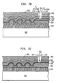
- Figure 7B shows a cross-sectional view of the semiconductor wafer 200 in accordance with an alternative embodiment of the present invention.
- the fluorine doped HDP oxide layer 402 is replaced with a phosphorous (P) doped HDP oxide layer 712.
- the phosphorous doped HDP oxide layer 722 is preferably deposited to a thickness of between about 100 angstroms and about 2,000 angstroms, and more preferably between about 300 angstroms and about 1,000 angstroms, and most preferably, about 500 angstroms.
- the concentration of phosphorous is preferably selected to be between about 3% wt. and about 20% wt., and more preferably between about 6% wt.
- the phosphorous doped HDP oxide layer 712 provides a good etch-stop signal 714 when etching commences into layer 712 at a point 702 within the terminal via (TV).
- the etch stop signal will be in the form of an increase detection of phosphorous atoms within the plasma etching chamber.
- an HDP-type oxide is deposited for layer 712, other oxides, such as a CVD oxide and PECVD oxide may also be deposited as a doped material with the above-identified concentrations.
- Figure 7C shows a cross-sectional view of the semiconductor wafer 200 in accordance with yet another alternative embodiment of the present invention.
- the phosphorous (P) doped HDP oxide layer 712 is replaced with a tensile stress spin-on-glass (SOG) layer 722.
- the tensile stress SOG layer 722 is an Organix SOG available from Allied Signal of Sunnyvale, California, an Organic SOG available from Dow Corning of Auburn, Michigan, or any other SOG material having tensile stress or less compressive stress than a pure HDP oxide material.
- the tensile stress SOG layer 722 is preferably deposited to a thickness of between about 100 angstroms and about 2,000 angstroms, and more preferably between about 300 angstroms and about 1,000 angstroms, and most preferably, about 500 angstroms.
- the tensile stress SOG layer is cured before the HDP oxide layer 502 is deposited.
- the tensile stress SOG layer 722 provides a good etch-stop physical barrier during terminal via (TV) formation when a selective plasma etching operation is performed.
- the tensile stress SOG layer 722 serves to both reduce the compressive stress of the intermetal dielectrics ( i.e ., layers 302, 502 and 602) and provides a good physical etch stop.
- the physical etch stop will ensure that at least between about 500 angstroms and about 5,000 angstroms, and more preferably between about 1,000 angstroms and 3,000 angstroms, and most preferably about 2,000 angstroms of oxide remains over a metal fuse structure (e.g ., that may be patterned from metallization layer 204).
Landscapes
- Physics & Mathematics (AREA)
- Engineering & Computer Science (AREA)
- Plasma & Fusion (AREA)
- Chemical & Material Sciences (AREA)
- Analytical Chemistry (AREA)
- Internal Circuitry In Semiconductor Integrated Circuit Devices (AREA)
- Semiconductor Memories (AREA)
- Design And Manufacture Of Integrated Circuits (AREA)
- Drying Of Semiconductors (AREA)
Claims (24)
- Verfahren zum Ausbilden eines Anschlußdurchkontakts in einer Fuse-Struktur (204b) umfassend:Ausbilden der Fuse-Struktur (204b) aus einer Metallisierungsschicht (204);Abscheiden einer unteren Oxidschicht (302) über der Fuse-Struktur (204b) die aus der Metallisierungsschicht (204) ausgebildet ist,Abscheiden einer dotierten oxidschicht (402, 712) über der Basisoxidschicht (302);Abscheiden einer oberen Oxidschicht (602) über der dotierten Oxidschicht (402, 712);Ätzen durch die obere Oxidschicht (602);Detektieren eines erhöhten Niveaus einer Dotierstoffspezies, die emittiert wird, wenn die dotierte Oxidschicht (402, 712) zu ätzen beginnt; undBeenden der Ätzung, wenn das erhöhte Niveau an Dotierstoffspezies detektiert ist, derart, daß mindestens die untere Oxidschicht (302) über der Fuse-Struktur (204b) zurückbleibt, die aus der Metallisierungsschicht (204) ausgebildet ist.
- Verfahren zum Ausbilden eines Anschlußdurchkontakts in einer Fuse-Struktur (204b) nach Anspruch 1, wobei die untere Oxidschicht (302) eine Dicke von zwischen etwa 500 Ångström und etwa 2000 Ängström aufweist.
- Verfahren zum Ausbilden eines Anschlußdurchkontakts in einer Fuse-Struktur (204b) nach Anspruch 2, wobei die dotierte Oxidschicht (402) ein hochdichtes Plasmaoxid ist, das mit einem Fluor-Dotierstoff dotiert ist.
- Verfahren zum Ausbilden eines Anschlußdurchkontakts in einer Fuse-Struktur (204b) nach Anspruch 2,
wobei die Fluorkonzentration zwischen etwa 2 Gew.-% und etwa 20 Gew.-% ausgewählt wird. - Verfahren zum Ausbilden eines Anschlußdurchkontakts in einer Fuse-Struktur (204b) nach Anspruch 2, wobei die dotierte Oxidschicht (712) ein hochdichtes Plasmaoxid ist, das mit einem Phosphor-Dotierstoff dotiert ist.
- Verfahren zum Ausbilden eines Anschlußdurchkontakts in einer Fuse-Struktur (204b) nach Anspruch 5, wobei die Phosphor-Konzentration zwischen etwa 3 Gew.-% und etwa 20 Gew.-% ausgewählt ist.
- Verfahren zum Ausbilden eines Anschlußdurchkontakts in einer Fuse-Struktur (204b) nach Anspruch 3,
wobei das Ätzen in einer Plasmaätzkammer unter Verwendung einer Ätzchemie ausgewählt aus der Gruppe aus einer CHF3/02-Chemie und einer CF4/Ar-Chemie durchgeführt wird. - Verfahren zum Ausbilden eines Anschlußdurchkontakts in einer Fuse-Struktur (204b) nach Anspruch 7, weiterhin umfassend:Setzen eines Drucks in der Plasmaätzkammer auf zwischen 20 mTorr und etwa 120 mTorr.
- Verfahren zum Ausbilden eines Anschlußdurchkontakts in einer Fuse-Struktur (204b) nach Anspruch 8, weiterhin umfassend:Setzen einer Temperatur in der Plasmaätzkammer auf zwischen etwa 5°C und etwa 30°C.
- Verfahren zum Ausbilden eines Anschlußdurchkontakts in einer Fuse-Struktur (204b) nach Anspruch 9,
wobei, wenn die CHF3/O2-Chemie ausgewählt ist, das Verfahren weiterhin folgendes umfaßt:Fließenlassen von CHF3 mit einer Rate von zwischen etwa 5 und etwa 20sccms; undFließenlassen von 02 mit einer Rate von zwischen etwa 0 und etwa 30sccms. - Verfahren zum Ausbilden eines Anschlußdurchkontakts in einer Fuse-Struktur (204b) nach Anspruch 9, wobei, wenn die CF4/Ar-Chemie ausgewählt ist, das Verfahren weiterhin folgendes umfaßt:Fließenlassen von CF4 mit einer Rate von zwischen etwa 40 und etwa 80sccms; undFließenlassen von Ar mit einer Rate von zwischen etwa 50 und etwa 200sccms.
- Verfahren zum Ausbilden eines Anschlußdurchkontakts in einer Fuse-Struktur (204b) nach Anspruch 9, wobei die Fuse-Struktur (204b) in einer DRAM-Schaltung ausgebildet wird.
- Metall-Fuse-Struktur umfassend:eine Fuse-Struktur (204b), die aus einer Metallisierungsschicht (204) strukturiert ist;eine Basisoxidschicht (302), die über der Fuse-Struktur (204b) liegt, wobei die Basisoxidschicht (302) eine Dicke von zwischen etwa 500 Angström und etwa 2000 Ångström aufweist;eine Ätzstoppsignalschicht (402, 712), die über der Basisoxidschicht (302) liegt;eine obere Oxidschicht (602), die über der Ätzstopsignalschicht (402, 712) liegt; undeinen Anschlußdurchkontakt der durch die obere Oxidschicht (602) definiert ist, die über der Fuse-Struktur (204b) liegt, derart, daß der Anschlußdurchkontakt nicht an der Ätzstopschicht (402, 712) vorbei definiert wird und die über der Fuse-Struktur (204b) liegende Basisoxidschicht (302) zurückbleibt.
- Metall-Fuse-Struktur nach Anspruch 13, wobei die über der Basisoxidschicht (302) liegende Ätzstopsignalschicht (402, 712) einen Zugstreß innerhalb eines Intermetalldielektrikumstapels liefert, die die Basisoxidschicht (302), die Ätzstopsignalschicht (402, 712) und die obere Oxidschicht (602) enthält.
- Metall-Fuse-Struktur nach Anspruch 14, wobei der Zugstreß Stressmigration in der Metallisierungsschicht (204) reduziert.
- Metall-Fuse-Struktur nach Anspruch 15, wobei die über der Basisoxidschicht (302) liegende Ätzstopsignalschicht (402, 712) ein dotiertes hochdichtes Plasmaoxid ist.
- Metall-Fuse-Struktur nach Anspruch 16, wobei das dotierte hochdichte Plasmaoxid (402) ausgewählt ist aus der Gruppe bestehend aus einem Fluor-dotierten hochdichten Plasmaoxid und einem Phosphor-dotierten hochdichten Plasma (712).
- Metall-Fuse-Struktur nach Anspruch 17, wobei das Fluor-dotierte hochdichte Plasmaoxid (402) eine Fluor-Dotierstoff-Konzentration von zwischen etwa 2 Gew.% und etwa 20 Gew.-% aufweist.
- Metall-Fuse-Struktur nach Anspruch 18, wobei das Phosphor-dotierte hochdichte Plasmaoxid (712) eine Fluor-Dotierstoff-Konzentration von zwischen etwa 3 Gew.% und etwa 20 Gew.-% aufweist.
- Metall-Fuse-Struktur nach Anspruch 13, wobei die Metall-Fuse-Struktur in einer DRAM-Schaltung ausgebildet wird.
- Metall-Fuse-Struktur, umfassend:eine Fuse-Struktur (204b), die aus einer Metallisierungsschicht (204) strukturiert ist;eine Basisoxidschicht (302), die über der Fuse-Struktur (204b) liegt, wobei die Basisoxidschicht (302) eine Dicke von zwischen etwa 500 Ångström und etwa 2000 Ängström aufweist;eine Aufschleuderglasätzstopschicht (722), die über der Basisoxidschicht (302) liegt;eine obere Oxidschicht (602), die über der Aufschleuderglasätzstopschicht (722)) liegt; undeinen Anschlußdurchkontakt der durch die obere Oxidschicht (602) definiert ist, die über der Fuse-Struktur (204b) liegt, derart, daß der Anschlußdurchkontakt nicht an der Aufschleuderglasätzstopschicht (722) vorbei definiert wird und die über der Fuse-Struktur (204b) liegende Basisoxidschicht (302) zurückbleibt.
- Metall-Fuse-Struktur nach Anspruch 21, wobei die über der Basisoxidschicht (302) liegende Aufschleuderglasätzstopschicht (722) einen Zugstreß innerhalb eines Intermetalldielektrikumstapels liefert, die die Basisoxidschicht (302), die Aufschleuderglasätzstopschicht (722) und die obere Oxidschicht (602) enthält.
- Metall-Fuse-Struktur nach Anspruch 22, wobei der Zugstreß Stressmigration in der Metallisierungsschicht (204) reduziert.
- Metall-Fuse-Struktur nach Anspruch 23, wobei die Metall-Fuse-Struktur in einer DRAM-Schaltung ausgebildet ist.
Applications Claiming Priority (2)
| Application Number | Priority Date | Filing Date | Title |
|---|---|---|---|
| US08/941,093 US5955380A (en) | 1997-09-30 | 1997-09-30 | Endpoint detection method and apparatus |
| US941093 | 1997-09-30 |
Publications (3)
| Publication Number | Publication Date |
|---|---|
| EP0905765A2 EP0905765A2 (de) | 1999-03-31 |
| EP0905765A3 EP0905765A3 (de) | 2002-08-21 |
| EP0905765B1 true EP0905765B1 (de) | 2007-08-08 |
Family
ID=25475906
Family Applications (1)
| Application Number | Title | Priority Date | Filing Date |
|---|---|---|---|
| EP98116749A Expired - Lifetime EP0905765B1 (de) | 1997-09-30 | 1998-09-04 | Endpunktfühlung und Apparat |
Country Status (7)
| Country | Link |
|---|---|
| US (1) | US5955380A (de) |
| EP (1) | EP0905765B1 (de) |
| JP (1) | JPH11163154A (de) |
| KR (1) | KR100567976B1 (de) |
| CN (1) | CN1150606C (de) |
| DE (1) | DE69838202T2 (de) |
| TW (1) | TW395028B (de) |
Families Citing this family (23)
| Publication number | Priority date | Publication date | Assignee | Title |
|---|---|---|---|---|
| TW442923B (en) * | 1998-03-20 | 2001-06-23 | Nanya Technology Corp | Manufacturing method of DRAM comprising redundancy circuit region |
| US6177286B1 (en) * | 1998-09-24 | 2001-01-23 | International Business Machines Corporation | Reducing metal voids during BEOL metallization |
| US6255207B1 (en) * | 1999-06-21 | 2001-07-03 | Taiwan Semiconductor Manufacturing Company | Composite planarizing dielectric layer employing high density plasma chemical vapor deposited (HDP-CVD) underlayer |
| US6306746B1 (en) * | 1999-12-30 | 2001-10-23 | Koninklijke Philips Electronics | Backend process for fuse link opening |
| US20020013044A1 (en) * | 2000-07-27 | 2002-01-31 | Mena Rafael A. | HDP liner layer prior to HSQ/SOG deposition to reduce the amount of HSQ/SOG over the metal lead |
| JP3551944B2 (ja) * | 2001-07-25 | 2004-08-11 | セイコーエプソン株式会社 | 半導体装置 |
| JP2004055876A (ja) * | 2002-07-22 | 2004-02-19 | Renesas Technology Corp | 半導体装置及び半導体装置の製造方法 |
| KR100885843B1 (ko) * | 2002-08-31 | 2009-02-27 | 엘지디스플레이 주식회사 | 유기전계발광 표시소자 및 그 제조방법 |
| US7067896B2 (en) | 2002-11-13 | 2006-06-27 | Taiwan Semiconductor Manufacturing Co., Ltd. | Microelectronic fabrication having edge passivated bond pad integrated with option selection device access aperture |
| US6827868B2 (en) * | 2002-11-27 | 2004-12-07 | International Business Machines Corporation | Thinning of fuse passivation after C4 formation |
| JP2005032916A (ja) * | 2003-07-10 | 2005-02-03 | Renesas Technology Corp | 半導体装置 |
| TW200810083A (en) * | 2006-06-09 | 2008-02-16 | Nxp Bv | A semiconductor fuse structure and a method of manufacturing a semiconductor fuse structure |
| CN100397609C (zh) * | 2006-08-04 | 2008-06-25 | 北京中星微电子有限公司 | 一种聚焦离子束修改集成电路的方法及集成电路 |
| US7491585B2 (en) * | 2006-10-19 | 2009-02-17 | International Business Machines Corporation | Electrical fuse and method of making |
| JP5696620B2 (ja) | 2011-08-22 | 2015-04-08 | 富士通セミコンダクター株式会社 | ヒューズ、半導体装置、半導体装置の製造方法 |
| US9556017B2 (en) | 2013-06-25 | 2017-01-31 | Analog Devices, Inc. | Apparatus and method for preventing stiction of MEMS devices encapsulated by active circuitry |
| US10081535B2 (en) | 2013-06-25 | 2018-09-25 | Analog Devices, Inc. | Apparatus and method for shielding and biasing in MEMS devices encapsulated by active circuitry |
| US10229878B2 (en) | 2014-08-08 | 2019-03-12 | Renesas Electronics Corporation | Semiconductor device |
| US9604841B2 (en) | 2014-11-06 | 2017-03-28 | Analog Devices, Inc. | MEMS sensor cap with multiple isolated electrodes |
| TWI677056B (zh) | 2018-04-16 | 2019-11-11 | 華邦電子股份有限公司 | 半導體裝置及其製造方法 |
| CN108573952A (zh) * | 2018-04-23 | 2018-09-25 | 上海华虹宏力半导体制造有限公司 | 半导体元件熔丝结构及其制造方法 |
| CN110416182B (zh) * | 2018-04-28 | 2021-01-29 | 华邦电子股份有限公司 | 半导体装置及其制造方法 |
| CN117766511A (zh) * | 2024-02-20 | 2024-03-26 | 芯联集成电路制造股份有限公司 | 熔丝结构及其制备方法、半导体集成电路及其制备方法 |
Family Cites Families (9)
| Publication number | Priority date | Publication date | Assignee | Title |
|---|---|---|---|---|
| EP0304729B1 (de) * | 1987-08-14 | 1993-03-17 | Fairchild Semiconductor Corporation | Bestimmung des Ätzungsendpunktes |
| JPH05235170A (ja) * | 1992-02-24 | 1993-09-10 | Nec Corp | 半導体装置 |
| US5565114A (en) * | 1993-03-04 | 1996-10-15 | Tokyo Electron Limited | Method and device for detecting the end point of plasma process |
| JP3255524B2 (ja) * | 1993-12-28 | 2002-02-12 | 三菱電機株式会社 | 冗長回路を有する半導体装置およびその製造方法 |
| JP4417439B2 (ja) * | 1994-06-29 | 2010-02-17 | フリースケール セミコンダクター インコーポレイテッド | エッチング・ストップ層を利用する半導体装置構造とその方法 |
| JP2713178B2 (ja) * | 1994-08-01 | 1998-02-16 | 日本電気株式会社 | 半導体記憶装置およびその製造方法 |
| KR0154766B1 (ko) * | 1994-12-09 | 1998-12-01 | 김광호 | 반도체장치의 접촉창 형성방법 |
| EP0762498A3 (de) * | 1995-08-28 | 1998-06-24 | International Business Machines Corporation | Fenster für Sicherung mit kontrollierter Sicherungsoxiddicke |
| KR100244793B1 (ko) * | 1996-05-01 | 2000-03-02 | 김영환 | 반도체 소자의 콘택홀 형성방법 |
-
1997
- 1997-09-30 US US08/941,093 patent/US5955380A/en not_active Expired - Lifetime
-
1998
- 1998-08-05 TW TW087112883A patent/TW395028B/zh not_active IP Right Cessation
- 1998-08-14 CN CNB981184286A patent/CN1150606C/zh not_active Expired - Fee Related
- 1998-09-04 DE DE69838202T patent/DE69838202T2/de not_active Expired - Fee Related
- 1998-09-04 EP EP98116749A patent/EP0905765B1/de not_active Expired - Lifetime
- 1998-09-29 KR KR1019980040451A patent/KR100567976B1/ko not_active Expired - Fee Related
- 1998-09-30 JP JP10279025A patent/JPH11163154A/ja not_active Withdrawn
Non-Patent Citations (1)
| Title |
|---|
| None * |
Also Published As
| Publication number | Publication date |
|---|---|
| CN1150606C (zh) | 2004-05-19 |
| CN1213165A (zh) | 1999-04-07 |
| DE69838202T2 (de) | 2008-05-29 |
| KR19990030226A (ko) | 1999-04-26 |
| US5955380A (en) | 1999-09-21 |
| JPH11163154A (ja) | 1999-06-18 |
| KR100567976B1 (ko) | 2006-05-25 |
| DE69838202D1 (de) | 2007-09-20 |
| TW395028B (en) | 2000-06-21 |
| EP0905765A3 (de) | 2002-08-21 |
| EP0905765A2 (de) | 1999-03-31 |
Similar Documents
| Publication | Publication Date | Title |
|---|---|---|
| US5955380A (en) | Endpoint detection method and apparatus | |
| US6515343B1 (en) | Metal-to-metal antifuse with non-conductive diffusion barrier | |
| US6307213B1 (en) | Method for making a fuse structure for improved repaired yields on semiconductor memory devices | |
| US6794694B2 (en) | Inter-wiring-layer capacitors | |
| US5461010A (en) | Two step etch back spin-on-glass process for semiconductor planarization | |
| US6287956B2 (en) | Multilevel interconnecting structure in semiconductor device and method of forming the same | |
| US8377819B2 (en) | Contact formation | |
| KR20010014901A (ko) | 집적회로용 대머신 커패시터 | |
| KR0138308B1 (ko) | 층간접촉구조 및 그 방법 | |
| US6017824A (en) | Passivation etching procedure, using a polysilicon stop layer, for repairing embedded DRAM cells | |
| US6509244B2 (en) | Method for forming storage node electrode using a polysilicon hard mask on a sacrificial insulation film | |
| US5607873A (en) | Method for forming contact openings in a multi-layer structure that reduces overetching of the top conductive structure | |
| US6724054B1 (en) | Self-aligned contact formation using double SiN spacers | |
| KR100270962B1 (ko) | 반도체 집적회로의 커패시터 제조방법 | |
| KR20000017148A (ko) | 반도체 장치 및 그 제조 방법 | |
| HK1017501A (en) | Endpoint detection method and apparatus | |
| KR100190055B1 (ko) | 반도체 장치의 백금전극 제조방법 | |
| KR100393965B1 (ko) | 반도체 소자의 캐패시터 및 그의 제조 방법 | |
| KR20010086025A (ko) | 티타늄 나이트라이드와 고밀도 플라즈마 산화막 사이의인터레이어 | |
| US6312983B1 (en) | Etching method for reducing bit line coupling in a DRAM | |
| KR100370130B1 (ko) | 반도체 소자의 제조방법 | |
| KR20050005972A (ko) | 반도체 소자의 제조방법 | |
| US6838371B2 (en) | Method of manufacturing semiconductor device | |
| KR100696774B1 (ko) | 반도체소자의 캐패시터 형성방법 | |
| US6610603B2 (en) | Method of manufacturing a capacitor |
Legal Events
| Date | Code | Title | Description |
|---|---|---|---|
| PUAI | Public reference made under article 153(3) epc to a published international application that has entered the european phase |
Free format text: ORIGINAL CODE: 0009012 |
|
| AK | Designated contracting states |
Kind code of ref document: A2 Designated state(s): AT BE CH CY DE DK ES FI FR GB GR IE IT LI LU MC NL PT SE |
|
| AX | Request for extension of the european patent |
Free format text: AL;LT;LV;MK;RO;SI |
|
| PUAL | Search report despatched |
Free format text: ORIGINAL CODE: 0009013 |
|
| AK | Designated contracting states |
Kind code of ref document: A3 Designated state(s): AT BE CH CY DE DK ES FI FR GB GR IE IT LI LU MC NL PT SE |
|
| AX | Request for extension of the european patent |
Free format text: AL;LT;LV;MK;RO;SI |
|
| RIC1 | Information provided on ipc code assigned before grant |
Free format text: 7H 01L 21/66 A, 7H 01J 37/32 B, 7H 01L 23/525 B |
|
| 17P | Request for examination filed |
Effective date: 20030125 |
|
| AKX | Designation fees paid |
Designated state(s): DE GB IE |
|
| 17Q | First examination report despatched |
Effective date: 20040316 |
|
| RAP1 | Party data changed (applicant data changed or rights of an application transferred) |
Owner name: INFINEON TECHNOLOGIES AG |
|
| REG | Reference to a national code |
Ref country code: HK Ref legal event code: WD Ref document number: 1017501 Country of ref document: HK |
|
| GRAP | Despatch of communication of intention to grant a patent |
Free format text: ORIGINAL CODE: EPIDOSNIGR1 |
|
| GRAS | Grant fee paid |
Free format text: ORIGINAL CODE: EPIDOSNIGR3 |
|
| GRAA | (expected) grant |
Free format text: ORIGINAL CODE: 0009210 |
|
| AK | Designated contracting states |
Kind code of ref document: B1 Designated state(s): DE GB IE |
|
| REG | Reference to a national code |
Ref country code: GB Ref legal event code: FG4D |
|
| REG | Reference to a national code |
Ref country code: IE Ref legal event code: FG4D |
|
| REF | Corresponds to: |
Ref document number: 69838202 Country of ref document: DE Date of ref document: 20070920 Kind code of ref document: P |
|
| PGFP | Annual fee paid to national office [announced via postgrant information from national office to epo] |
Ref country code: DE Payment date: 20071113 Year of fee payment: 10 |
|
| PLBE | No opposition filed within time limit |
Free format text: ORIGINAL CODE: 0009261 |
|
| STAA | Information on the status of an ep patent application or granted ep patent |
Free format text: STATUS: NO OPPOSITION FILED WITHIN TIME LIMIT |
|
| 26N | No opposition filed |
Effective date: 20080509 |
|
| GBPC | Gb: european patent ceased through non-payment of renewal fee |
Effective date: 20071108 |
|
| PG25 | Lapsed in a contracting state [announced via postgrant information from national office to epo] |
Ref country code: IE Free format text: LAPSE BECAUSE OF NON-PAYMENT OF DUE FEES Effective date: 20070904 |
|
| PG25 | Lapsed in a contracting state [announced via postgrant information from national office to epo] |
Ref country code: GB Free format text: LAPSE BECAUSE OF NON-PAYMENT OF DUE FEES Effective date: 20071108 |
|
| PG25 | Lapsed in a contracting state [announced via postgrant information from national office to epo] |
Ref country code: DE Free format text: LAPSE BECAUSE OF NON-PAYMENT OF DUE FEES Effective date: 20090401 |