EP0903752A2 - Nicht-flüchtige Halbleiter-Speicher-Vorrichtung - Google Patents
Nicht-flüchtige Halbleiter-Speicher-Vorrichtung Download PDFInfo
- Publication number
- EP0903752A2 EP0903752A2 EP98121757A EP98121757A EP0903752A2 EP 0903752 A2 EP0903752 A2 EP 0903752A2 EP 98121757 A EP98121757 A EP 98121757A EP 98121757 A EP98121757 A EP 98121757A EP 0903752 A2 EP0903752 A2 EP 0903752A2
- Authority
- EP
- European Patent Office
- Prior art keywords
- transistor
- current
- node
- memory cell
- gate
- Prior art date
- Legal status (The legal status is an assumption and is not a legal conclusion. Google has not performed a legal analysis and makes no representation as to the accuracy of the status listed.)
- Granted
Links
Images


Classifications
-
- G—PHYSICS
- G11—INFORMATION STORAGE
- G11C—STATIC STORES
- G11C16/00—Erasable programmable read-only memories
- G11C16/02—Erasable programmable read-only memories electrically programmable
- G11C16/06—Auxiliary circuits, e.g. for writing into memory
- G11C16/26—Sensing or reading circuits; Data output circuits
-
- G—PHYSICS
- G11—INFORMATION STORAGE
- G11C—STATIC STORES
- G11C16/00—Erasable programmable read-only memories
- G11C16/02—Erasable programmable read-only memories electrically programmable
- G11C16/06—Auxiliary circuits, e.g. for writing into memory
- G11C16/30—Power supply circuits
-
- G—PHYSICS
- G11—INFORMATION STORAGE
- G11C—STATIC STORES
- G11C29/00—Checking stores for correct operation ; Subsequent repair; Testing stores during standby or offline operation
- G11C29/04—Detection or location of defective memory elements, e.g. cell constructio details, timing of test signals
-
- G—PHYSICS
- G11—INFORMATION STORAGE
- G11C—STATIC STORES
- G11C29/00—Checking stores for correct operation ; Subsequent repair; Testing stores during standby or offline operation
- G11C29/52—Protection of memory contents; Detection of errors in memory contents
-
- G—PHYSICS
- G06—COMPUTING OR CALCULATING; COUNTING
- G06F—ELECTRIC DIGITAL DATA PROCESSING
- G06F2201/00—Indexing scheme relating to error detection, to error correction, and to monitoring
- G06F2201/81—Threshold
Definitions
- This invention relates to a nonvolatile semiconductor memory, particularly to an EPROM and an EEPROM including a nonvolatile memory circuit and, more particularly to a circuit construction of a nonvolatile semiconductor memory of the batch erasure type (hereinafter referred to as a flash memory).
- the invention further relates particularly to a circuit construction concerning a sense amplifying (S/A) circuit and a high speed reading operation in a nonvolatile semiconductor memory.
- S/A sense amplifying
- Fig. 2 of the accompanying drawings shows diagrammatically a structure of a cell used in a flash memory.
- V G is a gate terminal, at V D a drain terminal, at V S a source terminal, at 27 a control gate CG connected to the gate terminal V G , and at 25 a floating gate FG which is controlled by the potential of the control gate CG.
- a semiconductor substrate e.g., a semiconductor substrate having P-type conductivity.
- well portions 23, 24 made of semiconductor having N-type conductivity.
- the well portion 23 forms a drain while the well portion 24 forms a source.
- Indicated at 26, 28 are insulating films.
- the write verification and erase verification are carried out so as to confirm whether the degree of writing and the degree of erasing have a sufficient margin for the read voltage, i.e., a variation range of the normal supply voltage V CC (5V ⁇ 0.5V). Generally, these verifications are carried out to confirm that an operation margin of about O.5V to 1.0V is available for a voltage range of V CC . In this case, the verify voltage including the operation margin is 6V to 6.5V in the write verification, and 3.5V to 4V in the erase verification.
- the write verification and the erase verification can be accomplished easily if the verify voltage including the operation margin to be secured is applied to word lines (for example, word lines WL 1 to WL m of the flash memory shown in Fig. 1), so that the sensitivity of the S/A circuit is the same regardless of whether the voltage V CC or the verify voltage is applied as the supply voltage of the S/A circuit.
- word lines for example, word lines WL 1 to WL m of the flash memory shown in Fig. 1
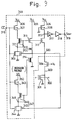
- Fig. 3 of the accompanying drawings shows a construction of a general S/A circuit used in the non-volatile semiconductor memory such as an EPROM.
- V CC is a line of a supply voltage 5V
- V SS a line of a supply voltage 0V.
- a gate of the transistor 11 is connected to power supply line V SS
- a gate of the transistor 12 is connected to a data line (i.e., a bit line).
- a data line i.e., a bit line.
- an n-channel transistor 13 whose gate is connected to drains of the respective transistors 11, 12.
- a p-channel transistor 14 and an n-channel transistor 15 in series.
- a gate of the transistor 14 is connected to the power supply line V SS
- a gate of the transistor 15 is connected to the drains of the respective transistors 11, 12.
- An output (data output) of the S/A circuit is taken from drains of the respective transistors 14, 15.
- the transistor 15 is provided with a function of transmitting the level of the bit line to the data output line (bit line level adjustment), and the transistor 14 is provided with a function of discriminating the data of the memory cell according to the state (on/off) of the transistor 15.
- An embodiment of the present invention pertains to a nonvolatile semiconductor memory including a sense amplifier for detecting a current, and an object thereof is to provide a nonvolatile semiconductor memory capable of shortening a reading time during a reading operation when a current flows through a memory cell transistor, to thereby carry out the reading operation at high speed.
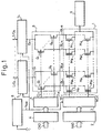
- a nonvolatile semiconductor memory comprising a cell matrix circuit (1) having erasable nonvolatile memory cell transistors (M ij ) arranged at intersections of a plurality of word lines (WL 1 to WL m ) and a plurality of bit lines (BL 11 to BL 1k , .., BL n1 to BL nk ); a row decoding circuit (3); a column decoding circuit (5); sense amplifying circuits (7 1 to 7 n ) connected to the respective bit lines (BL 11 to BL 1k , ..., BL n1 to BL nk ) of the cell matrix circuit (1).
- M ij erasable nonvolatile memory cell transistors
- Each of the said sense amplifying circuits includes load means and a first transistor for detecting a current arranged in series between a high voltage supply and one terminal of the bit line connected to the memory cell transistor; an output portion provided at a node of the load means and the first transistor; an inverter arranged between a gate of the first transistor and a terminal of the bit line; and a second transistor for amplifying the current arranged between the terminal of the bit line and a low voltage supply, a gate of the second transistor being connected to an output portion of the inverter.
- indicated at 1 is a cell array formed by arranging erasable nonvolatile memory cells M ij at intersections of a plurality of word lines WL 1 to WL m and a plurality of bit lines BL 11 to BL 1k , ..., BL n1 to BL nk .
- the cell array is divided into n blocks, in each of which (k ⁇ m) memory cells are arranged.
- Indicated at 2 is a row address buffer for buffering a row address RAD of an address signal fed externally thereto, at 3 a row decoder for decoding the row address and selecting any one of the word lines WL 1 to WL m , at 4 a column address buffer for buffering a column address CAD of the address signal, and at 5 a column decoder for decoding the column address and selecting any one of column lines CL 1 to CL k corresponding to the bit lines BLi 1 to BLi k for each of the aforementioned blocks.
- Indicated at 6 is a column gate circuit including transfer gate transistors Q 1 to Q k corresponding to the bit lines BL i1 to BL ik for each of the aforementioned blocks. The respective transistors Q 1 to Q k are turned on when the corresponding column lines CL 1 to CL k are selected, to thereby connect the selected bit line BL ij to a data line D i .
- Indicated at 7 1 to 7 n are respectively writing circuits and S/A circuits for applying amplification to a write data and sense amplification to a read data between corresponding internal data lines D 1 to D n and external input/output data lines I/O 1 to I/O n .
- Indicated at 8 is a verify source voltage generating circuit for generating a verify voltage V VER in accordance with a control signal C fed externally thereto. The generated verify source voltage V VER is supplied to the selected word lines WL 1 to WL m through the row decoder 3 as described later, and to the S/A circuit corresponding to the selected word line.
- Indicated at 9 is a source voltage supply circuit for supplying a source voltage in common to the respective sources of the nonvolatile memory cells M ij .
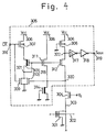
- Fig. 4 shows a basic portion of the structure of a sense amplifier used conventionally when the EPROM is, for example, used as a cell memory transistor in the nonvolatile semiconductor memory including a built-in sense amplifier of the current detecting type.
- a memory cell transistor at 302 a word line, at 303 a bit line, at 304 an n-MOS transistor of the enhancement type for selecting the bit line 303 in accordance with a bit line selection signal Y 0 , and at 305 a sense amplifier of the current detecting type.
- a power supply line for supplying a supply voltage V CC , at 307, 308 p-MOS transistors of the enhancement type, at 309 to 312 n-MOS transistors of the enhancement type, and at 313, 314 n-MOS transistors of the depletion type.
- the n-MOS transistors 310 and 313 constitute an inverter 315 of the so-called E/D (enhancement/depletion) type in which the n-MOS transistors 310, 313 are used as a drive transistor and a load transistor respectively.
- Indicated at 316 is a chip enable signal input terminal to which a chip enable signal /CE is input, at 317 a Schmidt trigger inverter, at 318 a normal inverter, and at 319 a sense amplifier output terminal from which a sense amplifier output Sout is output.
- the p-MOS transistor 307 and the n-MOS transistor 309 are transistors operable to make the sense amplifier 305 inactive (to be described later)in the case where this EPROM is not selected so that power is not consumed in the sense amplifier 305.
- the p-MOS transistor 308 is a load transistor for detecting whether a current flows through the selected memory cell transistor during the reading operation, and a gate thereof is grounded.
- the n-MOS transistor 314 is a transistor for supplementing the current flowing through the p-MOS transistor 308 so as to facilitate the current detection in the p-MOS transistor 308 since only a small amount of current flows through the selected memory cell transistor even when the selected memory cell transistor is turned on during the reading operation.
- n-MOS transistors 311, 312 and the inverter 315 are adapted to reduce the voltage at a node 320 when it increases, and to stabilize the same at, for example, 1V.
- a circuit constant is set such that when the voltage at the node 320 is higher than 1V, the potential at an output terminal of the inverter 315, namely a node 321, decreases to thereby reduce the amount of current flowing through the n-MOS transistors 311, 312, the voltage at the node 320 is stabilized at 1V.
- the circuit constant is also set such that the voltage at the node 322 becomes "H" relative to the Schmidt trigger inverter 317 when the voltage at the node 320 is 1V.
- the n-MOS transistor 311 also has function to speed up the charging operation to charge the bit-lines.
- the chip enable signal /CE becomes "H"; the p-MOS transistor 307 is turned off; and the n-MOS transistor 309 is turned on.
- the chip enable signal /CE becomes "L"; the p-MOS transistor 307 is turned on; and the n-MOS transistor 309 is turned off.
- the supply voltage V CC is supplied to the inverter 315 through the p-MOS transistor 307, and the n-MOS transistors 311 and 312 are turned on, thereby bringing the sense amplifier 305 into an active state.
- the voltage at the node 320 increases due to the current supplied through the p-MOS transistor 308 and the n-MOS transistor 312 and the current supplied through the n-MOS transistor 311.
- the voltage at the node 321 decreases to thereby reduce the amount of current flowing through the n-MOS transistors 311, 312, and the voltage at the node 320 is stabilized at 1V.
- the level of the node 322 becomes "H”, and "H” is output to the sense amplifier output terminal 319 as the sense amplifier output Sout.
- the n-MOS transistor 314 is provided to facilitate the current detection in the p-MOS transistor 308, and to supplement the current flowing through the p-MOS transistor 308 during the reading operation so as to carry out the reading operation at high speed. It is required in the commercial market to shorten a reading time further so as to carry out the reading operation at high speed in the case where the current flows through the selected memory cell transistor.
- an emodiment of the present invention seeks to provide a nonvolatile semiconductor memory including a sense amplifier for detecting a current which is capable of shortening a reading time to carry out a reading operation at high speed in the case where the current flows through a memory cell transistor during the reading operation.
- the sense amplifier used in the nonvolatile semiconductor memory is provided with a function of carrying out computational processing at a higher speed if a larger amount of current is caused to flow.
- the ability to drive the sense amplifier is suppressed.
- a basic concept of an embodiment of the present invention is to detect the level of the current flowing through the memory cell transistor by causing another current to flow simultaneously with the current flowing through the memory cell transistor.
- an embodiment of the present invention is directed to a nonvolatile semiconductor memory comprising a cell matrix circuit (1) having erasable nonvolatile memory cell transistors (M ij ) arranged at intersections of a plurality of word lines (WL 1 to WL m ) and a plurality of bit lines (BL 11 to BL 1k , ..., BL n1 to BL nk ); and sense amplifying circuits (7 1 to 7 n ) connected to the respective bit lines (BL 11 to BL 1k , ..., BL n1 to BL nk ), wherein each sense amplifying circuit includes load means and a first transistor for detecting a current arranged in series between a high voltage supply and one terminal of the bit line connected to the memory cell transistor; an output portion provided at a node of the load means and the first transistor; an inverter arranged between a gate of the first transistor and a terminal of the bit line; and a second transistor for amplifying the current arranged between the terminal
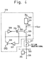
- Figs. 5 and 6 show a principle of the sense amplifier in an embodiment of the present invention.
- the reference numeral 324 denotes a memory cell transistor, 325 a word line, 326 a bit line, 327 a bit-line selecting switching device of which the on-off operation is controlled with a bit line select signal, and 328 ( Figure 5) and 329 ( Figure 6) sense amplifiers.
- the reference numeral 330 denotes a power line over which a power-supply voltage V CC is supplied, 331 a load intended for detection of whether or not a current flows through a selected memory cell transistor at the time of data reading, 332 a node at which sense amplifier output Sout develops, 333 to 335 n-channel MOS transistors and 336 and 337 ( Figure 6) inverters.
- the n-channel MOS transistor 333 is provided to supplement the current flowing to the load 331 in order to facilitate the detection of a current at the load 331 since the current flowing through the selected memory cell transistor is turned on at the time of data reading.
- the n-channel MOS transistors 334 and 335 and the inverter 336 are provided to stabilize at a predetermined level the voltage at the junction of the n-channel MOS transistor 335 and switching device 327, that is, the voltage at the node 338.
- n-channel MOS transistor 334 also serves to supplement the current flowing through the n-channel MOS transistor 333 when the selected memory cell transistor is turned off and thus no current flows through the memory cell transistor.
- the circuit is so designed that the voltage at the gate of the n-channel MOS transistor 333 is controlled to fall when the voltage at the node 338 rises at the time of data reading and to rise when the voltage at the node 338 falls at the time of data reading.
- Figs. 5 and 6 show example circuit configurations of embodiments of the present invention.
- Fig. 5 shows an example circuit configuration in which the inverter 336 is connected at the output terminal thereof to the gate of the n-channel MOS transistor 333
- Fig. 6 shows another example circuit configuration in which the inverter 337, different from the inverter 336 whose input terminal is connected to the node 338, is connected at the output terminal thereof to the gate of the n-channel MOS transistor 333.
- a flash-type memory embodying the present invention comprises the sense amplifier 328 or 329 having the first n-channel MOS transistor 335 connected at the drain thereof to the power line by means of the load 331 and at the source thereof to one terminal of a bit-line selecting switching device 327 (the other terminal of which is connected to the bit line 326); the first inverter 336 connected at the input terminal thereof to the node 338, that is, the junction of the first n-channel MOS transistor 335 and the switching device 327, and at the output terminal to the gate of the first n-channel MOS transistor 335; the second n-channel MOS transistor 334 connected at the drain thereof to the power line 330, at the source thereof to the node 338, that is, the junction of the first n-channel MOS transistor 335 and the switching device 327, and at the gate thereof to the output terminal of the first inverter 336; the third n-channel MOS transistor
- the n-channel MOS transistor 333 is so controlled that when the voltage at the node 338 falls, namely, when a current flows through a selected memory cell transistor at the time of data reading, the voltage at the gate of the n-channel MOS transistor 333 rises. Therefore, the current flowing through the load 331 can be increased to shorten the time taken for the signal "L" to develop at the sense amplifier output Sout, namely, the time taken for data reading when the current flows through the selected memory cell transistor, thereby permitting a higher data reading speed.
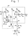
- Fig. 7 is a circuit diagram showing parts of a first embodiment of the present invention.
- the reference numeral 340 denotes a sense amplifier in which an n-channel MOS transistor 314 is connected at the gate thereof to the output terminal of an inverter 315.
- the remaining configuration is similar to that of the conventional EPROM shown in Fig. 4 .
- the n-channel MOS transistor 304 is turned off with the bit line select signal Yo taking the L level, the voltage at the node 320 becomes stable at 1V.
- the circuit constant is so set that in this case the voltage at the node 322 takes the H level with respect to the Schmidt-trigger inverter 317.
- the chip enable signal /CE takes the H level so that the p-channel MOS transistor 307 is turned off while the n-channel MOS transistor 309 is turned on.
- the chip enable signal /CE takes the L level so that the p-channel MOS transistor 307 is turned on while the n-channel MOS transistor 309 is turned off.
- Vcc is supplied again to the inverter 315 through the p-channel MOS transistor 307, and the n-channel MOS transistors 311 and 312 are turned on so that the sense amplifier is activated.
- the word line 302 takes the H level and the n-channel MOS transistor 304 is turned on(i.e. the bit line select signal Yo takes the H level) so that the memory cell transistor 301 is selected.
- the voltage at the node 320 rises due to the current supplied through the p-channel MOS transistor 308 and the n-channel MOS transistor 312 and the current supplied through the n-channel MOS transistor 311.
- the voltage at the node 321 then falls, the current flowing through the n-channel MOS transistors 311 and 312 decreases, the voltage at the node 320 becomes stable at 1V, the node 322 takes the H level, and a sense amplifier output Sout at the H level develops at the sense amplifier output terminal 319.
- the time required for the node 322 to take the L level can be shortened and the data reading can be effected at a high speed compared to the case that the n-channel MOS transistor 314 is connected at the gate thereof to the ground potential.
- the control circuit in this embodiment comprising the second transistor and inverter permits the time required for the node 322 to take the L level to be shortened as indicated with the waveform (A) and considerably shortens the time taken for data reading compared to the corresponding waveform (B) in the conventional circuit configuration.
- Fig. 8 is a circuit diagram showing parts of a second embodiment of the present invention.
- the reference numeral 341 denotes a sense amplifier comprising a power line 306 over which the power-supply voltage Vcc is supplied, an enhancement-type p-channel MOS transistor 343, enhancement-type n-channel MOS transistors 344 and 345, and a depletion-type n-channel MOS transistor 346.
- an E/D-type inverter 347 is made up of then-channel MOS transistor 345 ( drive transistor) and the n-channel MOS transistor 346 ( load transistor).
- this second embodiment has a circuit configuration that includes the p-channel MOS transistor 343, n-channel MOS transistor 344 and the inverter 347.
- the input terminal of the inverter 347 is connected to the node 320 and the n-channel MOS transistor 314 is connected at the gate thereof to the node 348.
- the second embodiment is similar to the first embodiment shown in Fig. 7.
- the n-channel MOS transistor 304 is turned on so that the memory cell transistor 301 is selected. If no current flows through the memory cell transistor 301, the voltage at the node 320 rises due to the current supplied through the p-channel MOS transistor 308 and n-channel MOS transistor 312 and the current supplied through the n-channel MOS transistor 311.
- the voltage at the node 321 then falls, the current flowing through the n-channel MOS transistors 311 and 312 decreases, the voltage at the node 320 becomes stable at 1V, the node 322 takes the H level and a sense amplifier output Sout at the H level develops at the sense amplifier output terminal 319.
- the time required for the node 322 to take the L level can be shortened and the data reading can be done at a high speed compared to the case that the n-channel MOS transistor 314 is connected at the gate thereof to the ground potential.
- Fig. 9 is a circuit diagram showing parts of a third embodiment of the present invention.
- the reference numeral 349 denotes a sense amplifier having a low voltage line 350, which supplies a low voltage VA produced by dropping the power-supply voltage Vcc.
- the circuit of this third embodiment is so configured that the low voltage VA is supplied through the p-channel MOS transistor 343 to the inverter 347, which will be operated with the low voltage VA.
- the third embodiment is similar to the second embodiment shown in Fig. 8.
- the third embodiment has a similar effect to that of the second embodiment. Furthermore, the rise of the voltage at the node 348 when the voltage at the node 320 falls is more limited than in the second embodiment. This has the effect of limiting the rise of the gate voltage of the n-channel MOS transistor 314, thereby preventing a fault from occurring as a result of the current flowing through the n-channel MOS transistor 314 becoming too large.
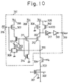
- Fig. 10 is a circuit diagram showing parts of a fourth embodiment of the present invention.
- the reference numeral 351 denotes a sense amplifier comprising an n-channel MOS transistor 352 connected at the drain thereof to the power line 306, at the source thereof to the node 322 and supplied at the gate thereof with an ATD signal.
- this fourth embodiment is similar to the first embodiment shown in Fig. 7.
- the status with the H level can be read at a higher speed.
- the n-channel MOS transistor 314 is connected at the gate thereof to the node 321 as in the first embodiment, so that when the voltage at the node 320 falls at the time of data reading, the gate voltage of the n-channel MOS transistor 314 rises and the current flowing through the n-channel MOS transistor 314 increases.
- the time required for the node 322 to take the L level can be shortened and the data reading can be done at a high speed compared to the case when the n-channel MOS transistor 314 is connected at the gate thereof to the ground potential.
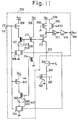
- Fig. 11 is a circuit diagram showing parts of a fifth embodiment of the present invention.
- the reference numeral 353 denotes a sense amplifier comprising an MOS transistor 352 connected at the drain thereof to the power line 306, at the source thereof to the node 322 and supplied at the gate thereof with an ATD signal.
- this fifth embodiment is similar to the second embodiment shown in Fig. 8.
- the nodes 320 and 322 are precharged based on the ATD signal so that no current flows through a selected memory cell transistor at the time of data reading, the status with the H level can be read at a higher speed.
- the n-channel MOS transistor 314 is connected at the gate thereof to the node 348 as in the second embodiment, so that when the voltage at the node 320 falls at the time of data reading, the gate voltage of the n-channel MOS transistor 314 rises and the current flowing through the n-channel MOS transistor 314 increases.
- the time required for the node 322 to take the L level can be shortened and the data reading can be done at a high speed compared to the case when the n-channel MOS transistor 314 is connected at the gate thereof to the ground potential.
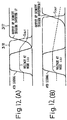
- Fig. 12 is a waveform diagram showing the operation of the sense amplifier 353 as shown in Fig. 11 used in the fifth embodiment in comparison with the operation of the conventional sense amplifier 305 shown in Fig. 4 .
- Fig. 12 (A) is a waveform diagram showing the operation of the sense amplifier 353 as shown in Fig. 11, incorporated in the fifth embodiment, and
- Fig. 12 (B) is a waveform diagram showing the operation of the sense amplifier 305 shown in Fig. 4.
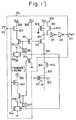
- Fig. 13 is a circuit diagram showing parts of a sixth embodiment of the present invention.
- the reference numeral 354 denotes a sense amplifier comprising an n-channel MOS transistor 352 connected at the drain thereof to the power line 306, at the source thereof to the node 322 and supplied at the gate thereof with an ATD signal.
- the sixth embodiment is similar to the third embodiment shown in Fig. 9.
- the n-channel MOS transistor 314 is connected at the gate thereof to the node 348 as in the third embodiment, so that when the voltage at the node 320 falls at the time of data reading, the gate voltage of the n-channel MOS transistor 314 rises and the current flowing through the n-channel MOS transistor 314 increases.
- the time required for the node 322 to take the L level can be shortened and the data reading can be done at a high speed as compared to the case when the n-channel MOS transistor 314 is connected at the gate thereof to the ground potential.
- the inverter 347 is supplied with a low voltage VA.
- VA the voltage at the node 320 falls
- the rise of the gate voltage of the n-channel MOS transistor 314 is limited more than in the fifth embodiment in decreasing the current through the n-channel MOS transistor 314, thereby preventing a fault from occuring as a result of the current flowing through the n-channel MOS transistor 314 becoming too large.
- the n-channel MOS transistor that supplements the current flowing through the load has a rise in its gate voltage.
- the current through the load is increased so that the time required for data reading when the current flows through the selected memory cell transistor can be shortened and the data reading can be effected at a higher speed.
Landscapes
- Read Only Memory (AREA)
Applications Claiming Priority (7)
| Application Number | Priority Date | Filing Date | Title |
|---|---|---|---|
| JP3346663A JP2732471B2 (ja) | 1991-12-27 | 1991-12-27 | 不揮発性半導体記憶装置 |
| JP346663/91 | 1991-12-27 | ||
| JP34666391 | 1991-12-27 | ||
| JP19179392 | 1992-07-20 | ||
| JP191793/92 | 1992-07-20 | ||
| JP19179392A JPH0636581A (ja) | 1992-07-20 | 1992-07-20 | 半導体記憶装置 |
| EP92311829A EP0549374B1 (de) | 1991-12-27 | 1992-12-29 | Nicht-flüchtiger Halbleiterspeicher |
Related Parent Applications (1)
| Application Number | Title | Priority Date | Filing Date |
|---|---|---|---|
| EP92311829A Division EP0549374B1 (de) | 1991-12-27 | 1992-12-29 | Nicht-flüchtiger Halbleiterspeicher |
Publications (3)
| Publication Number | Publication Date |
|---|---|
| EP0903752A2 true EP0903752A2 (de) | 1999-03-24 |
| EP0903752A3 EP0903752A3 (de) | 1999-04-28 |
| EP0903752B1 EP0903752B1 (de) | 2001-11-14 |
Family
ID=26506902
Family Applications (1)
| Application Number | Title | Priority Date | Filing Date |
|---|---|---|---|
| EP98121757A Expired - Lifetime EP0903752B1 (de) | 1991-12-27 | 1992-12-29 | Nicht-flüchtige Halbleiter-Speicher-Vorrichtung |
Country Status (2)
| Country | Link |
|---|---|
| EP (1) | EP0903752B1 (de) |
| DE (1) | DE69232210T2 (de) |
Cited By (1)
| Publication number | Priority date | Publication date | Assignee | Title |
|---|---|---|---|---|
| CN112837717A (zh) * | 2019-11-25 | 2021-05-25 | 补丁科技股份有限公司 | 用来在存储器模块中增加数据预取数量的装置 |
Family Cites Families (3)
| Publication number | Priority date | Publication date | Assignee | Title |
|---|---|---|---|---|
| US4823031A (en) * | 1988-02-01 | 1989-04-18 | Texas Instruments Incorporated | Single-ended sense amplifier with positive feedback |
| JPH03241594A (ja) * | 1990-02-19 | 1991-10-28 | Fujitsu Ltd | 半導体メモリのセンス回路 |
| JPH04238197A (ja) * | 1991-01-22 | 1992-08-26 | Nec Corp | センスアンプ回路 |
-
1992
- 1992-12-29 EP EP98121757A patent/EP0903752B1/de not_active Expired - Lifetime
- 1992-12-29 DE DE1992632210 patent/DE69232210T2/de not_active Expired - Fee Related
Cited By (1)
| Publication number | Priority date | Publication date | Assignee | Title |
|---|---|---|---|---|
| CN112837717A (zh) * | 2019-11-25 | 2021-05-25 | 补丁科技股份有限公司 | 用来在存储器模块中增加数据预取数量的装置 |
Also Published As
| Publication number | Publication date |
|---|---|
| EP0903752A3 (de) | 1999-04-28 |
| EP0903752B1 (de) | 2001-11-14 |
| DE69232210T2 (de) | 2002-05-02 |
| DE69232210D1 (de) | 2001-12-20 |
Similar Documents
| Publication | Publication Date | Title |
|---|---|---|
| US7518903B2 (en) | Semiconductor memory device and semiconductor integrated circuit system | |
| US7821829B2 (en) | Nonvolatile memory device including circuit formed of thin film transistors | |
| KR100261737B1 (ko) | 불휘발성 반도체 기억 장치 | |
| US8339852B2 (en) | Non-volatile memory device | |
| KR900003932B1 (ko) | 개량된 기입확인 동작 반도체 메모리장치 | |
| JP2001057088A (ja) | Nand型不揮発性メモリ | |
| US20030072176A1 (en) | Nonvolatile memory for which program operation is optimized by controlling source potential | |
| JP2002373495A (ja) | 半導体チップ、半導体集積回路装置及び半導体集積回路装置の製造方法 | |
| JP3920943B2 (ja) | 不揮発性半導体記憶装置 | |
| US7453742B2 (en) | Semiconductor integrated circuit device | |
| US6947325B2 (en) | Non-volatile semiconductor memory device and controlling method of the same | |
| KR960000345B1 (ko) | Eeprom 및 eeprom 독출 방법 | |
| JP3615009B2 (ja) | 半導体記憶装置 | |
| US5483485A (en) | Nonvolatile semiconductor system with automatic over erase protection | |
| EP0903752B1 (de) | Nicht-flüchtige Halbleiter-Speicher-Vorrichtung | |
| KR940005695B1 (ko) | 불휘발성 기억소자의 로우 디코더 회로 | |
| JP2732471B2 (ja) | 不揮発性半導体記憶装置 | |
| JPH05225791A (ja) | 電気的消去可能でプログラム可能なリードオンリメモリ | |
| JP2006311579A (ja) | 検知回路 | |
| JPH09306191A (ja) | 不揮発性半導体記憶装置 | |
| JP2659227B2 (ja) | Mos型不揮発性半導体メモリ装置 | |
| JP4302123B2 (ja) | 半導体集積回路装置 | |
| KR20230056198A (ko) | 메모리 셀 독출 회로 | |
| JPH05182483A (ja) | 不揮発性半導体記憶装置 |
Legal Events
| Date | Code | Title | Description |
|---|---|---|---|
| PUAI | Public reference made under article 153(3) epc to a published international application that has entered the european phase |
Free format text: ORIGINAL CODE: 0009012 |
|
| PUAL | Search report despatched |
Free format text: ORIGINAL CODE: 0009013 |
|
| AC | Divisional application: reference to earlier application |
Ref document number: 549374 Country of ref document: EP |
|
| AK | Designated contracting states |
Kind code of ref document: A2 Designated state(s): DE FR GB IT |
|
| AK | Designated contracting states |
Kind code of ref document: A3 Designated state(s): DE FR GB IT |
|
| 17P | Request for examination filed |
Effective date: 19990628 |
|
| 17Q | First examination report despatched |
Effective date: 20000323 |
|
| GRAG | Despatch of communication of intention to grant |
Free format text: ORIGINAL CODE: EPIDOS AGRA |
|
| GRAG | Despatch of communication of intention to grant |
Free format text: ORIGINAL CODE: EPIDOS AGRA |
|
| GRAH | Despatch of communication of intention to grant a patent |
Free format text: ORIGINAL CODE: EPIDOS IGRA |
|
| GRAH | Despatch of communication of intention to grant a patent |
Free format text: ORIGINAL CODE: EPIDOS IGRA |
|
| ITF | It: translation for a ep patent filed | ||
| GRAA | (expected) grant |
Free format text: ORIGINAL CODE: 0009210 |
|
| AC | Divisional application: reference to earlier application |
Ref document number: 549374 Country of ref document: EP |
|
| AK | Designated contracting states |
Kind code of ref document: B1 Designated state(s): DE FR GB IT |
|
| REF | Corresponds to: |
Ref document number: 69232210 Country of ref document: DE Date of ref document: 20011220 |
|
| REG | Reference to a national code |
Ref country code: GB Ref legal event code: IF02 |
|
| PLBE | No opposition filed within time limit |
Free format text: ORIGINAL CODE: 0009261 |
|
| STAA | Information on the status of an ep patent application or granted ep patent |
Free format text: STATUS: NO OPPOSITION FILED WITHIN TIME LIMIT |
|
| 26N | No opposition filed | ||
| PGFP | Annual fee paid to national office [announced via postgrant information from national office to epo] |
Ref country code: GB Payment date: 20071227 Year of fee payment: 16 Ref country code: FR Payment date: 20071210 Year of fee payment: 16 |
|
| PGFP | Annual fee paid to national office [announced via postgrant information from national office to epo] |
Ref country code: IT Payment date: 20071228 Year of fee payment: 16 Ref country code: DE Payment date: 20071231 Year of fee payment: 16 |
|
| GBPC | Gb: european patent ceased through non-payment of renewal fee |
Effective date: 20081229 |
|
| REG | Reference to a national code |
Ref country code: FR Ref legal event code: ST Effective date: 20090831 |
|
| PG25 | Lapsed in a contracting state [announced via postgrant information from national office to epo] |
Ref country code: DE Free format text: LAPSE BECAUSE OF NON-PAYMENT OF DUE FEES Effective date: 20090701 |
|
| PG25 | Lapsed in a contracting state [announced via postgrant information from national office to epo] |
Ref country code: GB Free format text: LAPSE BECAUSE OF NON-PAYMENT OF DUE FEES Effective date: 20081229 |
|
| PG25 | Lapsed in a contracting state [announced via postgrant information from national office to epo] |
Ref country code: FR Free format text: LAPSE BECAUSE OF NON-PAYMENT OF DUE FEES Effective date: 20081231 |
|
| PG25 | Lapsed in a contracting state [announced via postgrant information from national office to epo] |
Ref country code: IT Free format text: LAPSE BECAUSE OF NON-PAYMENT OF DUE FEES Effective date: 20081229 |