EP0888892A2 - Plaque d'orifices et procédé de fabrication, pour appareil d'ejection - Google Patents
Plaque d'orifices et procédé de fabrication, pour appareil d'ejection Download PDFInfo
- Publication number
- EP0888892A2 EP0888892A2 EP98112306A EP98112306A EP0888892A2 EP 0888892 A2 EP0888892 A2 EP 0888892A2 EP 98112306 A EP98112306 A EP 98112306A EP 98112306 A EP98112306 A EP 98112306A EP 0888892 A2 EP0888892 A2 EP 0888892A2
- Authority
- EP
- European Patent Office
- Prior art keywords
- orifice plate
- plate
- manufacturing
- liquid
- conductive
- Prior art date
- Legal status (The legal status is an assumption and is not a legal conclusion. Google has not performed a legal analysis and makes no representation as to the accuracy of the status listed.)
- Granted
Links
- 239000007788 liquid Substances 0.000 title claims abstract description 124
- 238000000034 method Methods 0.000 title claims abstract description 92
- 238000004519 manufacturing process Methods 0.000 title claims abstract description 51
- 238000007599 discharging Methods 0.000 title claims abstract description 19
- 239000011521 glass Substances 0.000 claims abstract description 37
- 239000004020 conductor Substances 0.000 claims abstract description 31
- 238000007747 plating Methods 0.000 claims abstract description 27
- 230000015572 biosynthetic process Effects 0.000 claims abstract description 19
- 238000005323 electroforming Methods 0.000 claims abstract description 16
- PXHVJJICTQNCMI-UHFFFAOYSA-N Nickel Chemical compound [Ni] PXHVJJICTQNCMI-UHFFFAOYSA-N 0.000 claims description 91
- 229910052759 nickel Inorganic materials 0.000 claims description 45
- BQCADISMDOOEFD-UHFFFAOYSA-N Silver Chemical compound [Ag] BQCADISMDOOEFD-UHFFFAOYSA-N 0.000 claims description 44
- 229910052709 silver Inorganic materials 0.000 claims description 44
- 239000004332 silver Substances 0.000 claims description 44
- 239000000758 substrate Substances 0.000 claims description 22
- 239000000853 adhesive Substances 0.000 claims description 20
- 230000001070 adhesive effect Effects 0.000 claims description 20
- VYZAMTAEIAYCRO-UHFFFAOYSA-N Chromium Chemical compound [Cr] VYZAMTAEIAYCRO-UHFFFAOYSA-N 0.000 claims description 17
- KDLHZDBZIXYQEI-UHFFFAOYSA-N Palladium Chemical compound [Pd] KDLHZDBZIXYQEI-UHFFFAOYSA-N 0.000 claims description 16
- 229910052804 chromium Inorganic materials 0.000 claims description 15
- 239000011651 chromium Substances 0.000 claims description 15
- BASFCYQUMIYNBI-UHFFFAOYSA-N platinum Chemical compound [Pt] BASFCYQUMIYNBI-UHFFFAOYSA-N 0.000 claims description 12
- 238000005260 corrosion Methods 0.000 claims description 11
- 230000007797 corrosion Effects 0.000 claims description 11
- PCHJSUWPFVWCPO-UHFFFAOYSA-N gold Chemical compound [Au] PCHJSUWPFVWCPO-UHFFFAOYSA-N 0.000 claims description 11
- 229910052737 gold Inorganic materials 0.000 claims description 11
- 239000010931 gold Substances 0.000 claims description 11
- 239000000463 material Substances 0.000 claims description 11
- 229910000990 Ni alloy Inorganic materials 0.000 claims description 8
- 238000006243 chemical reaction Methods 0.000 claims description 8
- 229910052751 metal Inorganic materials 0.000 claims description 6
- 239000002184 metal Substances 0.000 claims description 6
- 229910052697 platinum Inorganic materials 0.000 claims description 6
- 229910000531 Co alloy Inorganic materials 0.000 claims description 5
- 229910001252 Pd alloy Inorganic materials 0.000 claims description 5
- 239000010941 cobalt Substances 0.000 claims description 4
- GUTLYIVDDKVIGB-UHFFFAOYSA-N cobalt atom Chemical compound [Co] GUTLYIVDDKVIGB-UHFFFAOYSA-N 0.000 claims description 4
- 229910052763 palladium Inorganic materials 0.000 claims description 4
- 229920002614 Polyether block amide Polymers 0.000 claims description 3
- 229910052581 Si3N4 Inorganic materials 0.000 claims description 3
- 238000004891 communication Methods 0.000 claims description 3
- 229920006332 epoxy adhesive Polymers 0.000 claims description 3
- HQVNEWCFYHHQES-UHFFFAOYSA-N silicon nitride Chemical compound N12[Si]34N5[Si]62N3[Si]51N64 HQVNEWCFYHHQES-UHFFFAOYSA-N 0.000 claims description 3
- VYPSYNLAJGMNEJ-UHFFFAOYSA-N Silicium dioxide Chemical compound O=[Si]=O VYPSYNLAJGMNEJ-UHFFFAOYSA-N 0.000 claims description 2
- 229910052809 inorganic oxide Inorganic materials 0.000 claims description 2
- 229910044991 metal oxide Inorganic materials 0.000 claims description 2
- 229910000480 nickel oxide Inorganic materials 0.000 claims description 2
- 150000004767 nitrides Chemical class 0.000 claims description 2
- TWNQGVIAIRXVLR-UHFFFAOYSA-N oxo(oxoalumanyloxy)alumane Chemical compound O=[Al]O[Al]=O TWNQGVIAIRXVLR-UHFFFAOYSA-N 0.000 claims description 2
- GNRSAWUEBMWBQH-UHFFFAOYSA-N oxonickel Chemical compound [Ni]=O GNRSAWUEBMWBQH-UHFFFAOYSA-N 0.000 claims description 2
- BPUBBGLMJRNUCC-UHFFFAOYSA-N oxygen(2-);tantalum(5+) Chemical compound [O-2].[O-2].[O-2].[O-2].[O-2].[Ta+5].[Ta+5] BPUBBGLMJRNUCC-UHFFFAOYSA-N 0.000 claims description 2
- 229910052814 silicon oxide Inorganic materials 0.000 claims description 2
- 229910001936 tantalum oxide Inorganic materials 0.000 claims description 2
- 238000000206 photolithography Methods 0.000 abstract description 4
- 239000011159 matrix material Substances 0.000 description 12
- 239000011248 coating agent Substances 0.000 description 4
- 238000000576 coating method Methods 0.000 description 4
- 238000007796 conventional method Methods 0.000 description 4
- 238000012545 processing Methods 0.000 description 4
- 238000004070 electrodeposition Methods 0.000 description 3
- 238000010894 electron beam technology Methods 0.000 description 3
- 238000007639 printing Methods 0.000 description 3
- 229910021586 Nickel(II) chloride Inorganic materials 0.000 description 2
- 238000005299 abrasion Methods 0.000 description 2
- 239000007767 bonding agent Substances 0.000 description 2
- KGBXLFKZBHKPEV-UHFFFAOYSA-N boric acid Chemical compound OB(O)O KGBXLFKZBHKPEV-UHFFFAOYSA-N 0.000 description 2
- 239000004327 boric acid Substances 0.000 description 2
- 239000003638 chemical reducing agent Substances 0.000 description 2
- 238000009826 distribution Methods 0.000 description 2
- 239000000428 dust Substances 0.000 description 2
- 230000000694 effects Effects 0.000 description 2
- 230000005684 electric field Effects 0.000 description 2
- 238000005530 etching Methods 0.000 description 2
- 238000010438 heat treatment Methods 0.000 description 2
- 239000003112 inhibitor Substances 0.000 description 2
- 150000002500 ions Chemical class 0.000 description 2
- 230000001788 irregular Effects 0.000 description 2
- 230000005499 meniscus Effects 0.000 description 2
- QMMRZOWCJAIUJA-UHFFFAOYSA-L nickel dichloride Chemical compound Cl[Ni]Cl QMMRZOWCJAIUJA-UHFFFAOYSA-L 0.000 description 2
- KERTUBUCQCSNJU-UHFFFAOYSA-L nickel(2+);disulfamate Chemical compound [Ni+2].NS([O-])(=O)=O.NS([O-])(=O)=O KERTUBUCQCSNJU-UHFFFAOYSA-L 0.000 description 2
- 230000003287 optical effect Effects 0.000 description 2
- 239000002245 particle Substances 0.000 description 2
- 238000000059 patterning Methods 0.000 description 2
- 238000004321 preservation Methods 0.000 description 2
- 230000036647 reaction Effects 0.000 description 2
- 229920005989 resin Polymers 0.000 description 2
- 239000011347 resin Substances 0.000 description 2
- 229910052710 silicon Inorganic materials 0.000 description 2
- 239000010703 silicon Substances 0.000 description 2
- 238000012360 testing method Methods 0.000 description 2
- 235000010627 Phaseolus vulgaris Nutrition 0.000 description 1
- 244000046052 Phaseolus vulgaris Species 0.000 description 1
- QXZUUHYBWMWJHK-UHFFFAOYSA-N [Co].[Ni] Chemical compound [Co].[Ni] QXZUUHYBWMWJHK-UHFFFAOYSA-N 0.000 description 1
- 238000004026 adhesive bonding Methods 0.000 description 1
- 239000000919 ceramic Substances 0.000 description 1
- 238000005516 engineering process Methods 0.000 description 1
- 230000002708 enhancing effect Effects 0.000 description 1
- 239000000835 fiber Substances 0.000 description 1
- 239000010985 leather Substances 0.000 description 1
- 239000007769 metal material Substances 0.000 description 1
- 150000001455 metallic ions Chemical class 0.000 description 1
- BSIDXUHWUKTRQL-UHFFFAOYSA-N nickel palladium Chemical compound [Ni].[Pd] BSIDXUHWUKTRQL-UHFFFAOYSA-N 0.000 description 1
- 230000003647 oxidation Effects 0.000 description 1
- 238000007254 oxidation reaction Methods 0.000 description 1
- 239000004033 plastic Substances 0.000 description 1
- NNFCIKHAZHQZJG-UHFFFAOYSA-N potassium cyanide Chemical compound [K+].N#[C-] NNFCIKHAZHQZJG-UHFFFAOYSA-N 0.000 description 1
- XTFKWYDMKGAZKK-UHFFFAOYSA-N potassium;gold(1+);dicyanide Chemical compound [K+].[Au+].N#[C-].N#[C-] XTFKWYDMKGAZKK-UHFFFAOYSA-N 0.000 description 1
- 239000005871 repellent Substances 0.000 description 1
- 238000004544 sputter deposition Methods 0.000 description 1
- 239000000126 substance Substances 0.000 description 1
- 239000004753 textile Substances 0.000 description 1
- 239000002023 wood Substances 0.000 description 1
Images


Classifications
-
- B—PERFORMING OPERATIONS; TRANSPORTING
- B41—PRINTING; LINING MACHINES; TYPEWRITERS; STAMPS
- B41J—TYPEWRITERS; SELECTIVE PRINTING MECHANISMS, i.e. MECHANISMS PRINTING OTHERWISE THAN FROM A FORME; CORRECTION OF TYPOGRAPHICAL ERRORS
- B41J2/00—Typewriters or selective printing mechanisms characterised by the printing or marking process for which they are designed
- B41J2/005—Typewriters or selective printing mechanisms characterised by the printing or marking process for which they are designed characterised by bringing liquid or particles selectively into contact with a printing material
- B41J2/01—Ink jet
- B41J2/135—Nozzles
- B41J2/16—Production of nozzles
- B41J2/1621—Manufacturing processes
- B41J2/1625—Manufacturing processes electroforming
-
- B—PERFORMING OPERATIONS; TRANSPORTING
- B41—PRINTING; LINING MACHINES; TYPEWRITERS; STAMPS
- B41J—TYPEWRITERS; SELECTIVE PRINTING MECHANISMS, i.e. MECHANISMS PRINTING OTHERWISE THAN FROM A FORME; CORRECTION OF TYPOGRAPHICAL ERRORS
- B41J2/00—Typewriters or selective printing mechanisms characterised by the printing or marking process for which they are designed
- B41J2/005—Typewriters or selective printing mechanisms characterised by the printing or marking process for which they are designed characterised by bringing liquid or particles selectively into contact with a printing material
- B41J2/01—Ink jet
- B41J2/135—Nozzles
- B41J2/16—Production of nozzles
- B41J2/162—Manufacturing of the nozzle plates
-
- B—PERFORMING OPERATIONS; TRANSPORTING
- B41—PRINTING; LINING MACHINES; TYPEWRITERS; STAMPS
- B41J—TYPEWRITERS; SELECTIVE PRINTING MECHANISMS, i.e. MECHANISMS PRINTING OTHERWISE THAN FROM A FORME; CORRECTION OF TYPOGRAPHICAL ERRORS
- B41J2/00—Typewriters or selective printing mechanisms characterised by the printing or marking process for which they are designed
- B41J2/005—Typewriters or selective printing mechanisms characterised by the printing or marking process for which they are designed characterised by bringing liquid or particles selectively into contact with a printing material
- B41J2/01—Ink jet
- B41J2/135—Nozzles
- B41J2/16—Production of nozzles
- B41J2/1621—Manufacturing processes
- B41J2/164—Manufacturing processes thin film formation
- B41J2/1643—Manufacturing processes thin film formation thin film formation by plating
-
- B—PERFORMING OPERATIONS; TRANSPORTING
- B41—PRINTING; LINING MACHINES; TYPEWRITERS; STAMPS
- B41J—TYPEWRITERS; SELECTIVE PRINTING MECHANISMS, i.e. MECHANISMS PRINTING OTHERWISE THAN FROM A FORME; CORRECTION OF TYPOGRAPHICAL ERRORS
- B41J2202/00—Embodiments of or processes related to ink-jet or thermal heads
- B41J2202/01—Embodiments of or processes related to ink-jet heads
- B41J2202/03—Specific materials used
Definitions
- the present invention relates to a method for manufacturing an orifice plate for use of a liquid discharge that discharges a desired liquid by the creation of bubbles generated by the application of thermal energy or the like. It also relates to an orifice plate manufactured by such method of manufacture, a method for manufacturing a liquid discharge provided with such orifice plate, and a liquid discharge manufactured by such method of manufacture.
- the present invention is applicable to a printer, a copying machine, a facsimile equipment provided with communication system, a word processor provided with a printing unit, and some other apparatuses. It also applicable to an industrial recording system having various processing apparatuses combined comlexly therefor to make it possible to record on a recording medium, such as paper, thread, fiber, cloths, leather, metal, plastic, glass, wood, ceramic, or the like.
- the term "recording” referred to in the specification hereof means not only the provision of characters, graphics, or some other images that present some meaning when recorded on a recording medium, but also, means the provision of images that do not present any particular meaning, such as patterns recorded on the recording medium.
- 61-59911 and Japanese Patent Publication No. 61-59914 among some others.
- this recording method it is possible to record high quality images at high speeds in a lesser amount of noises.
- the bubble jet recording method has been widely used for office equipment, such as a printer, a copying machine, or a facsimile equipment in recent years. This method has been utilized also for a textile printing apparatus, and other industrial recording systems as well.
- the ink discharge port are formed on an orifice plate.
- the orifice plate is adhesively bonded to the liquid discharge main body side by the application of adhesive or the like subsequent to the discharge port having been formed on it.
- Figs. 17A to 17C are views which illustrate the steps of manufacture in accordance with the conventional method for manufacturing an orifice plate.
- the resist 307 is formed in a specific position on the substrate 301 (Fig. 17A).
- nickel 308 is formed by use of electroforming (Fig. 17B).
- the resist 307 and the substrate 301 are peeled off from the nickel 308 one after another in that order in order to form the discharge port 302 (Fig. 17C).
- the face pattern of the kind is obtainable by the irradiation of excimer laser on the resin sheet.
- the resist is formed in advance on the portion where the discharge port is formed, and then, by use of the electroforming, nickel is formed in order to provide the orifice plate. After that, the discharge port are formed by peeling off the resist from the nickel. As a result, the step 310 is inevitably formed on the discharge port as shown in Fig. 17C. This formation of such step 310 is not desirable for the performance of effective ink discharges.
- the corner portion 311 formed by the step 310 makes it easier for discharging droplets to reside on that portion to cause the loss of discharge energy accordingly.
- Ni or other metallic material for the orifice plate.
- the portion on the elemental substrate having the orifice plate, the ceiling plate, and the heaters arranged on it, which is in contact with ink, should be formed by metal or some other conductive material from the viewpoint of its manufacture, the liquid discharge and such portion become electrically conductive through ink (by the direct contact or through the adhesive) to present a cell structure which may in some cases satisfy the condition that allows electrolytic corrosion to occur.
- the inventors hereof have taken up as one of the new subjects that the reliability of the orifice plate should be made invariable and more stabilized for a longer period.
- the inner structure may become electrically conductive, not necessarily directly as described above, but depending on the components contained in the liquid.
- the condition of electrolytic corrosion may be satisfied depending on some metallic ion or other ion contained in the liquid as the case may be.
- An ion of the kind may inevitably exist in the liquid flow paths due to the structure of liquid container serving as the supply-source of liquid or due to the unprepared supply of liquid other than the designated one. Therefore, it becomes a second subject to be taken up by the inventors hereof that even in such a case as described above, the reliability of the orifice plate should be made invariable and stabilized for a longer period.
- the present invention is designed. It is an object of the invention to provide a method for manufacturing an orifice plate capable of discharging liquid droplets stably, while materializing the provision of high quality images, as well as presenting the chemical stability thereof even when electroforming is used, and also, to provide an orifice plate manufactured by such method of manufacture, a method for manufacturing a liquid discharge having such orifice plate therefor, and a liquid discharge manufactured by such method of manufacture as well.
- the method of the present invention for manufacturing an orifice plate used for a liquid discharge provided with discharge port for discharging liquid comprises the following steps of:
- the orifice plate of the present invention used for a liquid discharge having discharge port for discharging liquid, which is formed by nickel is provided with a protection layer having a higher resistance to corrosion than nickel being formed on the surface of the orifice plate on the ink discharge side.
- a method of the present invention for manufacturing a liquid discharge provided with a plurality of discharge port for discharging liquid, an orifice plate provided with the discharge port, a plurality of liquid flow paths conductively connected with the discharge port, a plurality of energy generating devices arranged for the liquid flow paths to generate energy to be utilized for discharging liquid, and a substrate provided with the energy generating devices comprises the following steps of:
- the glass grooves are patterned with the chromium which is electron bean etched on the glass plate as the mask, and plating is made with silver being buried in the glass grooves.
- the orifice plate is formed, thus making it possible to materialize the same precision as in the case of adoption of the glass mask used for photolithography. Therefore, the variation of the orifice areas is made smaller to make the highly densified formation of orifices possible.
- the discharge port are formed without using resist, there is no possibility that any step is formed with respect to the discharge port. Therefore, it becomes possible to avoid any difficulty that may hinder the effectiveness of discharge energy acting upon discharging liquid droplets or to prevent the discharge directivity from being varied.
- the photolithographing steps are not adopted in order to manufacture orifice plates at lower costs.
- the sectional configuration of the discharge port shows the slanted form to make it easier to hold meniscus for the implementation of more stabilized liquid discharges and the enhancement of refilling capability as well.
- the chromium which is electron-beam etched on the glass plate, is used as the mask to pattern the glass grooves. Then, after the glass grooves are nickel plated with silver being buried in them, the nickel is further plated with a coating material having a higher resistant to corrosion than the nickel. As a result, even if silicon or metal is used for the elemental substrate provided with heater members on it, and the ceiling plate provided with flow paths formed for it, there is no possibility that the orifice plate is dissolved due to the formation of the cell reaction.
- the resist pattern is formed on the matrix, and after being nickel plated, the nickel is peeled off from the matrix. Then, on the surface on the matrix side, the protection layer is formed with the material having a higher resistance to corrosion than the nickel. In this case, too, it is possible to obtain the same effect as described above, hence presenting no possibility that the orifice plate is dissolved due to the cell structure.
- Figs. 1A to 1L are views which illustrate each of the steps of a method for manufacturing an orifice plate in accordance with one embodiment of the present invention
- Figs. 1A to 1E are plan views
- Figs. 1F to 1J are cross-sectional views, taken along lines 1F - 1F to 1J - 1J
- Fig. 1K and Fig. 1L are partially enlarged views, respectively.
- the silver mirror reaction occurs on the glass plate on which the pattern grooves of an orifice plate are patterned in high precision. Then, nickel is plated subsequent to rubbing off silver into the patterned grooved on the glass plate so that silver remains in them, hence manufacturing the orifice plate.
- the orifice plate thus manufactured is bonded to the liquid discharge of the edge shooter type.
- chromium is filmed on the glass, and resist is patterned by means of the EB etching. Then, chromium is etched to produce the chrome pattern. With chromium as mask, glass is etched to form the patterned grooves of an orifice plate. In this way, the glass plate 1 is produced (Figs. 1A and 1F).
- nickel 4 is developed in a thickness of 10 ⁇ m on the portions where silver 3 remain to make the nickel plating (Figs. 1D and 11).
- the nickel 4 plated orifice plate 10 is peeled off from the glass plate 1 to complete the orifice plate 10 (Figs. 1E and 1J).
- the diameter of the discharge port thus formed is 16 ⁇ m ⁇ 3%.
- Fig. 2 is a perspective view which shows an apparatus used for the plating process of the method for manufacturing an orifice plate represented in Figs. 1A to 1L.
- nickel sulfamate is used together with an applied reducer, zeol (manufactured by the World Metal K.K.), boric acid, a pit inhibitor, NS-APS (manufactured by the World Metal K.K.), and nickel chloride.
- the electric field is applied in such a manner that the electrodes are connected on the anode side in the plating solution, while the electrodes having silver 3 formed thereon are connected on the cathode side.
- the plating temperature is 50°C.
- the current density is 5A/dm 2 .
- Fig. 1C the portion indicated by slanted lines in Fig. 1C is the electrode unit to which the cathode is connected.
- nickel is plated. Besides, however, it may be possible to plate the silver portion 3 with gold, palladium, platinum, chromium, nickel-cobalt alloy, or nickel-palladium alloy.
- Fig. 3 is a perspective view which shows the external appearance of the orifice plate manufactured by the method represented in Figs. 1A to 1L.
- nickel Since no resist is used for the method of manufacture shown in Figs. 1A to 1L, nickel is allowed to be developed isotropically so that its section becomes to represent the rounded form as shown in Fig. 3.
- Fig. 4 is a view which shows one assembling step of the orifice plate, which is manufactured by the method represented in Figs. 1A to 1L, to a liquid discharge.
- adhesive 6 is coated on the orifice plate 10. Then, the orifice plate 10 having the adhesive 6 coated thereon is bonded to the face surface of the liquid discharge having the liquid flow paths 104, the elemental substrate 100 provided with the heating member 103, and the ceiling plate 109 formed for the head.
- Figs. 5A to 5D are views which illustrate the configuration of the liquid discharge provided with the orifice plate manufactured by the method represented in Figs. 1A to 1L;
- Fig. 5A is a perspective view which shows the external appearance thereof;
- Fig. 5B is a partially enlarged view which shows the portion 5B in Fig. 5A;
- Fig. 5C is a cross-sectional view, taken along line 5C - 5C in Fig. 5B;
- Fig. 5D is a partially enlarged view which shows the portion 5D in Fig. 5C.
- the orifice plate 10 is bonded to the face surface of the liquid discharge. After that, the assembled body is incorporated in an ink cartridge 120. Thus, as shown in Figs. 5A to 5D, the liquid discharge is completed.
- the edge of the pattern 124 having discharge port being formed in a specific position on the orifice plate as shown in Fig. 5D, becomes a rounded form 125 when the edge near the discharge port is lost at the time of distribution and in the initial stage of use. At the same time, the surface becomes irregular.
- This formation is made when the face is wiped by the blade for removing dust particles and ink adhering to the face as well. Also, the adhesion of ink may encroach on the face to result in such formation.
- the pattern 124 which is provided with the hydrophilic property, is continuously arranged, it becomes possible to provide a wider area serving as the ink trapping region and enhance the ink trapping capability accordingly, while making it difficult for the ink, which adheres to the face surface, to enter the discharge port.
- Fig. 6 is a view which shows one assembling step of the orifice plate, which is manufactured by the method represented in Figs. 1A to 1L, to a liquid discharge of the side shooter type.
- Fig. 7 is a view which shows the configuration of the liquid discharge of the side shooter type provided with the orifice plate manufactured by the method represented in Figs. 1A to 1L.
- the adhesive 6 is coated on the orifice plate 10. Then, the orifice plate 10 having the discharge port 5 arranged therefor is bonded to the liquid discharge provided with the liquid flow paths 104, the elemental substrate 100, and the ink supply path 119.
- the adhesive is coated on the orifice plate side when it is bonded to the liquid discharge.
- the adhesive it may be possible to coat the adhesive on the face surface side for the liquid discharge shown in Fig. 4 or on the elemental substrate 100 side for the liquid discharge shown in Fig. 6.
- the two-part adhesive which is an epoxy adhesive (CS-2340-5: manufactured by the Cemedain K.K.) or the polyether amide adhesive (HIMAL: manufactured by Hitachi Kasei K.K.) is used.
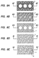
- Figs. 8A to 8L are views which illustrate each of the steps of a method for manufacturing an orifice plate in accordance with one embodiment of the present invention
- Figs. 8A to 8E are plan views
- Figs. 8F to 8J are cross-sectional views, taken along lines 8F - 8F to 8J - 8J
- Fig. 8K and Fig. 8L are partially enlarged views, respectively.
- the silver mirror reaction occurs on the glass plate on which the pattern grooves of an orifice plate are patterned in high precision. Then, nickel is plated subsequent to rubbing off silver into the patterned grooved on the glass plate so that silver remains in them, thus manufacturing the orifice plate.
- the orifice plate thus manufactured is bonded to the liquid discharge of the edge shooter type.
- chromium is filmed on the glass, and resist is patterned by means of the EB etching. Then, chromium is etched to produce the chrome pattern. With chromium as mask, glass is etched to form the patterned grooves 2 of an orifice plate. In this way, the glass plate 1 is produced (Figs. 8A and 8F).
- nickel 4 is developed in a thickness of 10 ⁇ m on the portions where silver remain to make the nickel plating, and then, the gold 7 plating is made on the nickel 4 by used of electroforming so as to make it a coating member (Figs. 8D and 8I).
- the nickel 4 plated orifice plate 10 is peeled off from the glass plate 1 to complete the orifice plate 10 (Figs. 8E and 8J).
- the diameter of the discharge opening 5 thus formed is 16 ⁇ m ⁇ 3%.
- nickel sulfamate As the plating solution for nickel, nickel sulfamate is used together with an applied reducer, zeol (manufactured by the World Metal K.K.), boric acid, a pit inhibitor, NS-APS (manufactured by the World Metal K.K.), and nickel chloride.
- zeol manufactured by the World Metal K.K.
- boric acid boric acid
- NS-APS manufactured by the World Metal K.K.
- nickel chloride As the one for gold, potassium gold cyanide or potassium cyanide is used.
- the electric field is applied in such a manner that the electrodes are connected on the anode side in the plating solution, while the electrodes having silver 3 formed thereon are connected on the cathode side.
- the plating temperature is 50°C.
- the current density is 5A/dm 2 .
- the electrodes are connected on the anode side in the plating solution, while the electrodes having nickel 4 formed on them are connected on the cathode side.
- the plating temperature is 65°C, and the current density is 4A/dm 2 .
- Fig. 8C the portion indicated by slanted lines in Fig. 8C is the electrode unit to which the cathode is connected.
- Fig. 9 is a view which shows one assembling step of the orifice plate, which is manufactured by the method represented in Figs. 8A to 8L, to a liquid discharge.
- bonding agent 6 is coated on the orifice plate 10. Then, the orifice plate 10 having the bonding agent 6 coated thereon is bonded to the face surface of the liquid discharge provided with the liquid flow paths 104, the elemental substrate 100, and the ceiling plate 109 formed therefor.
- Figs. 10A to 10D are views which illustrate the configuration of the liquid discharge provided with the orifice plate manufactured by the method represented in Figs. 8A to 8L;
- Fig. 10A is a perspective view shows the external appearance thereof;
- Fig. 10B is a partially enlarged view which shows the portion 10B in Fig. 10A;
- Fig. 10C is a cross-sectional view, taken along line 10C - 10C in Fig. 10B;
- Fig. 10D is a partially enlarged view which shows the portion 10D in Fig. 10C.
- the orifice plate 10 is bonded to the face surface of the liquid discharge. After that, the assembled body is incorporated in an ink cartridge 120. Thus, as shown in Figs. 10A to 10D, the liquid discharge is completed.
- the edge of the pattern 124 having discharge port being formed in a specific position on the orifice plate as shown in Fig. 10D, becomes a rounded form as at 125 when the edge near the discharge port is lost at the time of distribution and in the initial stage of use. At the same time, the surface becomes irregular.
- This formation is made when the face is wiped by the blade for removing dust particles and ink adhering to the face as well. Also, the adhesion of ink may corrode on the face to result in such formation.
- the preservation test is carried out by use of ink, with the result that no cell reaction occurs to cause any corrosion on the orifice plate manufactured in accordance with the present embodiment.
- gold 7 is used as the coating material.
- the present invention is not necessarily limited to it. If only the material to be used has a higher resistance to corrosion than the material used for the orifice plate formation (such as nickel used for the present embodiment).
- the orifice plate is made applicable to a head of the side shooter type.
- Fig. 11 is a view which shows one assembling step of the orifice plate, which is manufactured by the method represented in Figs. 8A to 8L, to a liquid discharge of the side shooter type.
- the adhesive 6 is coated on the orifice plate 10. Then, the orifice plate 10 having the discharge port 5 arranged therefor is bonded to the liquid discharge provided with the liquid flow paths 104, the elemental substrate 100 provided with the heating member 103, and the ink supply path 119.
- Figs. 12A to 12F are views which illustrate one embodiment of the method for manufacturing an orifice plate in accordance with the present invention
- Figs. 12A to 12C are plan views
- Figs. 12D to 12F are cross-sectional views, taken along lines 12D - 12D to 12F - 12F, respectively.
- resist 107 is patterned on a metallic matrix 112, and after nickel is plated, the orifice plate 108 formed by nickel is peeled off from the matrix 112, and then, a protection layer 8 is formed on the nickel surface on the matrix surface side.
- resist 107 is coated on the metallic (stainless) matrix 112, and patterning is carried out (Fig. 12A).
- the plating is made in the same condition as in the method of manufacture represented in Figs. 8A to 8L.
- the orifice plate 108 is peeled off from the matrix 112, and the protection layer 8 is formed on the matrix surface side of the orifice plate (Fig. 12C).
- silicon nitride is formed in a thickness of one ⁇ m by use of the sputtering method.
- an inorganic oxide a metallic oxide film, an inorganic nitride, or the like
- silicon oxide tantalum oxide, nickel oxide, aluminum oxide, silicon nitride, platinum, gold, or the like.
- the completed orifice plate is assembled to a liquid discharge, hence completing the head of the edge shooter type as shown in Figs. 13A to 13C or the head of the side shooter type as shown in Fig. 14.
- each of the orifice plates should be connected by use of leads if such method is adopted.
- a plurality of orifice plates are connected by leads and adhesively bonded to a highly smooth glass plate.
- the orifice plate thus manufactured may be adhesively bonded to the substrate of pressure generating devices, which is provided with grooved flow paths.
- the orifice plate manufactured by the method of the present invention provides each of its hole diameters in good precision so as to make it usable for all the ink jet recording apparatus.
- Figs. 13A to 13C are views which illustrate the configuration of a liquid discharge provided with the orifice plate manufactured by the method represented in Figs. 12A to 12F;
- Fig. 13A is a perspective view which shows the external appearance;
- Fig. 13B is a partially enlarged view which shows the portion 13B in Fig. 13A;
- Fig. 13C is a cross-sectional view, taken along line 13C - 13C.
- Fig. 14 is a view which shows the configuration of the side shooter type liquid discharge provided with the orifice plate manufactured by the method represented in Figs. 12A to 12F.
- the preservation test is carried out, with the result that no orifice plate is corroded by the cell structure, and there is no problem as to the reliability of the orifice plate at all.
- the adhesive is coated on the orifice plate side when it is bonded to the liquid discharge.
- the adhesive it may be possible to coat the adhesive on the face surface side with respect to the liquid discharge shown in Fig. 9 or on the elemental substrate 100 side with respect to the liquid discharge shown in Fig. 11.
- the two-part adhesive which is an epoxy adhesive (CS-2340-5: manufactured by the Cemedain K.K.) or the polyether amide adhesive (HIMAL: manufactured by Hitachi Kasei K.K.) is used.
- the material used for the electroforming in the processing steps in Fig. 8D and Fig. 12B it is possible to use not only nickel, but also, to use the alloy of nickel and cobalt or the alloy of nickel and palladium. In this case, since the abrasion resistance of the orifice plate is made higher, the durability thereof is enhanced accordingly.
- the material may be gold, platinum, or chromium.
- the ink container (not shown) provided for the interior of the liquid discharge shown in Figs. 10A to 10D is arranged to be reusable by refilling ink when ink is consumed.
- Fig. 15 is a view which shows one embodiment of the liquid jet apparatus (IJRA) having the liquid discharge mounted on it.
- IJRA liquid jet apparatus
- a carriage HC the head cartridge where a liquid tank unit 70 and a liquid discharge head unit 60 are detachably mountable.
- the carriage HC can reciprocate as indicated by arrows a and b in the width direction of a recording medium 80 which is carried by recording medium carrier means.
- driving signals are supplied from driving signal supplying means (not shown) to the liquid discharge means on the carriage HC, ink or other liquid is discharged from the liquid discharge to the recording medium in accordance with such signals.
- a motor 81 serving as the driving source to drive the recording medium carrier means and the carriage HC as well; the gears 82 and 83 that transmit the driving power from the driving source to the carriage HC; and the carriage shaft 85, among some others.
- Fig. 16 is a view which schematically shows the full line head and its apparatus where a plurality of discharge ports are arranged over the recordable area of a recording medium.
- the full line head 61 of the present embodiment is arranged in a position shiftable to the recording medium 80.
- the carrier drum 90 is provided as means for carrying the recording medium.
- each of the liquid discharges and liquid jet apparatuses of the present invention applicable to any one of ink discharge methods, ink jet recording heads, and ink jet recording apparatuses, respectively, by use of recording ink serving as liquid to be discharged, not necessarily limited to the embodiments described above.
- the chromium which is electron-beam etched on the glass plate is used as the mask for patterning glass grooves.
- the glass grooves are plated with silver buried in them.
- the orifice plate is formed.
- the discharge port are formed without using resist, there is no possibility that any step is formed with respect to the discharge port. Therefore, it becomes possible to avoid any difficulty that may hinder the effectiveness of discharge energy acting upon discharging liquid droplets or to prevent the discharge directivity from being varied.
- the photolithographing steps are not adopted in order to manufacture orifice plates at lower costs.
- the sectional configuration of the discharge port presents the rounded form to make it easier to hold meniscus for the implementation of more stabilized liquid discharges and the enhancement of refilling capability as well.
- the chromium electron-beam etched on the glass plate is used as mask to pattern the glass grooves. Then, after the glass grooves are nickel plated with silver being buried in them, the nickel is further plated with a coating material having a higher resistant to corrosion than the nickel. As a result, even if silicon or metal is used for the elemental substrate having heater members formed thereon and the ceiling plate having flow paths formed, there is no possibility that the orifice plate is dissolved due to the formation of the cell structure.
- the resist pattern is formed on the matrix, and after being nickel plated, the nickel is peeled off from the matrix. Then, on the surface on the matrix side, the protection layer is formed with the material having a higher resistance to corrosion than the nickel. In this case, too, it is possible to obtain the same effect as described above.
- a method for manufacturing an orifice plate used for a liquid discharge provided with discharge port for discharging liquid comprises the steps of preparing a non-conductive plate having recessed portion formed on the circumference of the flat portion corresponding to the discharge port, forming a first conductive material peelable from the non-conductive plate only in the recessed portion of the non-conductive plate, forming a plate member by plating the first conductive material with a second conductive material by electroforming method after the formation of the first conductive material, and obtaining the orifice plate having the discharge port by peeling off the plate member from the non-conductive plate.
Landscapes
- Engineering & Computer Science (AREA)
- Manufacturing & Machinery (AREA)
- Particle Formation And Scattering Control In Inkjet Printers (AREA)
Applications Claiming Priority (9)
| Application Number | Priority Date | Filing Date | Title |
|---|---|---|---|
| JP17829297 | 1997-07-03 | ||
| JP178292/97 | 1997-07-03 | ||
| JP17829297 | 1997-07-03 | ||
| JP22965397 | 1997-08-26 | ||
| JP22965397 | 1997-08-26 | ||
| JP229653/97 | 1997-08-26 | ||
| JP10178817A JPH11129483A (ja) | 1997-07-03 | 1998-06-25 | 液体吐出ヘッド用オリフィスプレートの製造方法、オリフィスプレート、該オリフィスプレートを有する液体吐出ヘッド及び液体吐出ヘッドの製造方法 |
| JP178817/98 | 1998-06-25 | ||
| JP17881798 | 1998-06-25 |
Publications (3)
| Publication Number | Publication Date |
|---|---|
| EP0888892A2 true EP0888892A2 (fr) | 1999-01-07 |
| EP0888892A3 EP0888892A3 (fr) | 2000-06-14 |
| EP0888892B1 EP0888892B1 (fr) | 2004-10-06 |
Family
ID=27324556
Family Applications (1)
| Application Number | Title | Priority Date | Filing Date |
|---|---|---|---|
| EP98112306A Expired - Lifetime EP0888892B1 (fr) | 1997-07-03 | 1998-07-02 | Plaque d'orifices et procédé de fabrication, pour appareil d'ejection |
Country Status (8)
| Country | Link |
|---|---|
| US (1) | US6328420B1 (fr) |
| EP (1) | EP0888892B1 (fr) |
| JP (1) | JPH11129483A (fr) |
| CN (1) | CN1089693C (fr) |
| AT (1) | ATE278554T1 (fr) |
| AU (1) | AU749988B2 (fr) |
| CA (1) | CA2242819C (fr) |
| DE (1) | DE69826769T2 (fr) |
Families Citing this family (8)
| Publication number | Priority date | Publication date | Assignee | Title |
|---|---|---|---|---|
| US6494563B2 (en) | 1997-12-25 | 2002-12-17 | Canon Kabushiki Kaisha | Ink jet element substrate and ink jet head that employs the substrate, and ink jet apparatus on which the head is mounted |
| US7178896B2 (en) * | 2003-01-29 | 2007-02-20 | Hewlett-Packard Development Company, L.P. | Article of manufacture including a two-part adhesive with a fluorescent dye and method of making |
| US20050206679A1 (en) * | 2003-07-03 | 2005-09-22 | Rio Rivas | Fluid ejection assembly |
| US20070097176A1 (en) * | 2005-10-31 | 2007-05-03 | Kenneth Hickey | Orifice plate coated with palladium nickel alloy |
| JP2007230194A (ja) * | 2006-03-03 | 2007-09-13 | Canon Finetech Inc | インクジェット記録ヘッドおよび製造方法 |
| US9409394B2 (en) | 2013-05-31 | 2016-08-09 | Stmicroelectronics, Inc. | Method of making inkjet print heads by filling residual slotted recesses and related devices |
| EP3342593B1 (fr) | 2015-09-28 | 2019-10-09 | Kyocera Corporation | Plaque de buse, tête d'éjection de liquide utilisant celle-ci, et dispositif d'enregistrement |
| CN110055567B (zh) * | 2019-04-18 | 2021-05-07 | 中国科学院化学研究所 | 微孔膜材料的电沉积制备方法和微孔膜材料及其应用 |
Citations (2)
| Publication number | Priority date | Publication date | Assignee | Title |
|---|---|---|---|---|
| JPS6159914A (ja) | 1984-08-31 | 1986-03-27 | Fujitsu Ltd | デイジタル圧縮装置 |
| JPS6159911A (ja) | 1984-08-30 | 1986-03-27 | Nec Corp | 切換スイツチ回路 |
Family Cites Families (19)
| Publication number | Priority date | Publication date | Assignee | Title |
|---|---|---|---|---|
| FR955987A (fr) | 1946-11-27 | 1950-01-23 | ||
| GB1499876A (en) | 1975-02-07 | 1978-02-01 | Emi Ltd | Methods of electroforming meshes or screens |
| US4184925A (en) * | 1977-12-19 | 1980-01-22 | The Mead Corporation | Solid metal orifice plate for a jet drop recorder |
| IT1159032B (it) * | 1983-06-10 | 1987-02-25 | Olivetti & Co Spa | Testina di stampa a getto selettivo d inchiostro |
| US4773971A (en) | 1986-10-30 | 1988-09-27 | Hewlett-Packard Company | Thin film mandrel |
| JPS63297050A (ja) | 1987-05-29 | 1988-12-05 | Seiko Epson Corp | バブルジェットヘッド用ノズル板 |
| JPS63309462A (ja) | 1987-06-11 | 1988-12-16 | Seiko Epson Corp | バブルジェットヘッド用ノズル板 |
| US4847630A (en) | 1987-12-17 | 1989-07-11 | Hewlett-Packard Company | Integrated thermal ink jet printhead and method of manufacture |
| EP0441503B1 (fr) | 1990-01-25 | 1994-04-13 | Canon Kabushiki Kaisha | Tête d'enregistrement par jet d'encre, substrat pour cette tête et dispositif d'enregistrement par jet d'encre |
| US5277783A (en) | 1991-05-15 | 1994-01-11 | Brother Kogyo Kabushiki Kaisha | Manufacturing method for orifice plate |
| JPH05510A (ja) | 1991-06-24 | 1993-01-08 | Brother Ind Ltd | オリフイスプレートの製造方法 |
| US5434606A (en) | 1991-07-02 | 1995-07-18 | Hewlett-Packard Corporation | Orifice plate for an ink-jet pen |
| JPH0577423A (ja) | 1991-09-24 | 1993-03-30 | Canon Inc | インクジエツト記録ヘツド |
| JP3206246B2 (ja) * | 1993-09-27 | 2001-09-10 | 富士ゼロックス株式会社 | 微小穴を有する金属部材の製造方法 |
| JP3169037B2 (ja) * | 1993-10-29 | 2001-05-21 | セイコーエプソン株式会社 | インクジェット記録ヘッドのノズルプレートの製造方法 |
| EP0713929B1 (fr) | 1994-10-28 | 1999-03-31 | SCITEX DIGITAL PRINTING, Inc. | Film mince sans chevilles pour mandrin permanent pour plaque d'orifice |
| JPH1024582A (ja) * | 1996-07-12 | 1998-01-27 | Canon Inc | 液体吐出ヘッド並びに該液体吐出ヘッドの回復方法及び製造方法、並びに該液体吐出ヘッドを用いた液体吐出装置 |
| JPH11238733A (ja) * | 1998-02-20 | 1999-08-31 | Sony Corp | 電子装置の製造方法およびこれを用いた電子装置 |
| JP4146932B2 (ja) * | 1998-06-03 | 2008-09-10 | キヤノン株式会社 | インクジェットヘッド |
-
1998
- 1998-06-25 JP JP10178817A patent/JPH11129483A/ja active Pending
- 1998-07-02 US US09/110,025 patent/US6328420B1/en not_active Expired - Fee Related
- 1998-07-02 DE DE69826769T patent/DE69826769T2/de not_active Expired - Fee Related
- 1998-07-02 EP EP98112306A patent/EP0888892B1/fr not_active Expired - Lifetime
- 1998-07-02 AT AT98112306T patent/ATE278554T1/de not_active IP Right Cessation
- 1998-07-02 AU AU74055/98A patent/AU749988B2/en not_active Ceased
- 1998-07-02 CA CA002242819A patent/CA2242819C/fr not_active Expired - Fee Related
- 1998-07-03 CN CN98115676.2A patent/CN1089693C/zh not_active Expired - Fee Related
Patent Citations (2)
| Publication number | Priority date | Publication date | Assignee | Title |
|---|---|---|---|---|
| JPS6159911A (ja) | 1984-08-30 | 1986-03-27 | Nec Corp | 切換スイツチ回路 |
| JPS6159914A (ja) | 1984-08-31 | 1986-03-27 | Fujitsu Ltd | デイジタル圧縮装置 |
Also Published As
| Publication number | Publication date |
|---|---|
| ATE278554T1 (de) | 2004-10-15 |
| AU7405598A (en) | 1999-01-14 |
| AU749988B2 (en) | 2002-07-04 |
| EP0888892A3 (fr) | 2000-06-14 |
| CN1204578A (zh) | 1999-01-13 |
| CA2242819A1 (fr) | 1999-01-03 |
| DE69826769D1 (de) | 2004-11-11 |
| US6328420B1 (en) | 2001-12-11 |
| CA2242819C (fr) | 2003-09-16 |
| DE69826769T2 (de) | 2006-03-09 |
| CN1089693C (zh) | 2002-08-28 |
| JPH11129483A (ja) | 1999-05-18 |
| EP0888892B1 (fr) | 2004-10-06 |
Similar Documents
| Publication | Publication Date | Title |
|---|---|---|
| US4775445A (en) | Process for producing a liquid jet recording head | |
| US6016601A (en) | Method of preparing the nozzle plate | |
| EP0249625B1 (fr) | Tete imprimante a jet d'encre ayant une plaque a orifice et a couche-barriere, et son procede de fabrication | |
| US4954225A (en) | Method for making nozzle plates | |
| EP0509669A2 (fr) | Plaque perforée pour têtes imprimantes à jet d'encre ainsi que son procédé de fabrication | |
| KR20060082412A (ko) | 액체 토출 헤드, 액체 토출 장치 및 액체 토출 헤드의 제조방법 | |
| US6328420B1 (en) | Method for manufacturing an orifice plate for use of a liquid discharge, an orifice plate, a liquid discharge provided with such orifice plate, and a method for manufacturing such liquid discharge | |
| KR100556008B1 (ko) | 프린트헤드,잉크카트리지,오리피스판보호방법및분리방법 | |
| EP0539993B1 (fr) | Tête d'impression à jet d'encre et son procédé de fabrication | |
| US6397466B1 (en) | Method for manufacturing orifice plate and liquid discharge head | |
| EP0999058B1 (fr) | Ensemble de plaques à buses pour micro-dispositif d'injection et procédé pour sa fabrication | |
| WO2009134263A1 (fr) | Revêtement de protection de fente d’alimentation | |
| JP3511762B2 (ja) | インクジェット記録ヘッドの製造方法 | |
| US6799832B1 (en) | Alloy and orifice plate for an ink-jet pen using the same | |
| JP3991405B2 (ja) | インクジェット記録ヘッド用ノズル板の製造方法 | |
| JP4015274B2 (ja) | インクジェットヘッド用ノズル板の製造方法 | |
| EP1354705B1 (fr) | Appareil d'éjection de liquide, tête d'imprimante, et procédé de production de l'appareil d'éjection de liquide | |
| JP2002001966A (ja) | 記録ヘッドと記録ヘッドの製造方法及びインクジェット記録装置 | |
| JP2002059551A (ja) | インクジェットノズル及びその製造方法 | |
| JP3127564B2 (ja) | インクジェットヘッド及びインクジェットヘッドの製造方法 | |
| JPH11300976A (ja) | 液体吐出ヘッド | |
| JP3190658B2 (ja) | インクジェット記録用ヘッド | |
| JP3554149B2 (ja) | 液体吐出ヘッドの製造方法 | |
| JP3568022B2 (ja) | インクジェットヘッドの製造方法 | |
| JP3166830B2 (ja) | 静電吸引型マルチノズルインクジェットヘッドの製造方法 |
Legal Events
| Date | Code | Title | Description |
|---|---|---|---|
| PUAI | Public reference made under article 153(3) epc to a published international application that has entered the european phase |
Free format text: ORIGINAL CODE: 0009012 |
|
| AK | Designated contracting states |
Kind code of ref document: A2 Designated state(s): AT BE CH DE DK ES FI FR GB GR IE IT LI LU MC NL PT SE |
|
| AX | Request for extension of the european patent |
Free format text: AL;LT;LV;MK;RO;SI |
|
| PUAL | Search report despatched |
Free format text: ORIGINAL CODE: 0009013 |
|
| AK | Designated contracting states |
Kind code of ref document: A3 Designated state(s): AT BE CH CY DE DK ES FI FR GB GR IE IT LI LU MC NL PT SE |
|
| AX | Request for extension of the european patent |
Free format text: AL;LT;LV;MK;RO;SI |
|
| RIC1 | Information provided on ipc code assigned before grant |
Free format text: 7B 41J 2/16 A, 7C 25D 1/08 B |
|
| 17P | Request for examination filed |
Effective date: 20001026 |
|
| AKX | Designation fees paid |
Free format text: AT BE CH DE DK ES FI FR GB GR IE IT LI LU MC NL PT SE |
|
| 17Q | First examination report despatched |
Effective date: 20010703 |
|
| GRAP | Despatch of communication of intention to grant a patent |
Free format text: ORIGINAL CODE: EPIDOSNIGR1 |
|
| GRAS | Grant fee paid |
Free format text: ORIGINAL CODE: EPIDOSNIGR3 |
|
| GRAA | (expected) grant |
Free format text: ORIGINAL CODE: 0009210 |
|
| AK | Designated contracting states |
Kind code of ref document: B1 Designated state(s): AT BE CH DE DK ES FI FR GB GR IE IT LI LU MC NL PT SE |
|
| PG25 | Lapsed in a contracting state [announced via postgrant information from national office to epo] |
Ref country code: NL Free format text: LAPSE BECAUSE OF FAILURE TO SUBMIT A TRANSLATION OF THE DESCRIPTION OR TO PAY THE FEE WITHIN THE PRESCRIBED TIME-LIMIT Effective date: 20041006 Ref country code: LI Free format text: LAPSE BECAUSE OF FAILURE TO SUBMIT A TRANSLATION OF THE DESCRIPTION OR TO PAY THE FEE WITHIN THE PRESCRIBED TIME-LIMIT Effective date: 20041006 Ref country code: IT Free format text: LAPSE BECAUSE OF FAILURE TO SUBMIT A TRANSLATION OF THE DESCRIPTION OR TO PAY THE FEE WITHIN THE PRESCRIBED TIME-LIMIT;WARNING: LAPSES OF ITALIAN PATENTS WITH EFFECTIVE DATE BEFORE 2007 MAY HAVE OCCURRED AT ANY TIME BEFORE 2007. THE CORRECT EFFECTIVE DATE MAY BE DIFFERENT FROM THE ONE RECORDED. Effective date: 20041006 Ref country code: FR Free format text: LAPSE BECAUSE OF NON-PAYMENT OF DUE FEES Effective date: 20041006 Ref country code: FI Free format text: LAPSE BECAUSE OF FAILURE TO SUBMIT A TRANSLATION OF THE DESCRIPTION OR TO PAY THE FEE WITHIN THE PRESCRIBED TIME-LIMIT Effective date: 20041006 Ref country code: CH Free format text: LAPSE BECAUSE OF FAILURE TO SUBMIT A TRANSLATION OF THE DESCRIPTION OR TO PAY THE FEE WITHIN THE PRESCRIBED TIME-LIMIT Effective date: 20041006 Ref country code: BE Free format text: LAPSE BECAUSE OF FAILURE TO SUBMIT A TRANSLATION OF THE DESCRIPTION OR TO PAY THE FEE WITHIN THE PRESCRIBED TIME-LIMIT Effective date: 20041006 Ref country code: AT Free format text: LAPSE BECAUSE OF FAILURE TO SUBMIT A TRANSLATION OF THE DESCRIPTION OR TO PAY THE FEE WITHIN THE PRESCRIBED TIME-LIMIT Effective date: 20041006 |
|
| REG | Reference to a national code |
Ref country code: GB Ref legal event code: FG4D |
|
| REG | Reference to a national code |
Ref country code: CH Ref legal event code: EP |
|
| REG | Reference to a national code |
Ref country code: IE Ref legal event code: FG4D |
|
| REF | Corresponds to: |
Ref document number: 69826769 Country of ref document: DE Date of ref document: 20041111 Kind code of ref document: P |
|
| PG25 | Lapsed in a contracting state [announced via postgrant information from national office to epo] |
Ref country code: SE Free format text: LAPSE BECAUSE OF FAILURE TO SUBMIT A TRANSLATION OF THE DESCRIPTION OR TO PAY THE FEE WITHIN THE PRESCRIBED TIME-LIMIT Effective date: 20050106 Ref country code: GR Free format text: LAPSE BECAUSE OF FAILURE TO SUBMIT A TRANSLATION OF THE DESCRIPTION OR TO PAY THE FEE WITHIN THE PRESCRIBED TIME-LIMIT Effective date: 20050106 Ref country code: DK Free format text: LAPSE BECAUSE OF FAILURE TO SUBMIT A TRANSLATION OF THE DESCRIPTION OR TO PAY THE FEE WITHIN THE PRESCRIBED TIME-LIMIT Effective date: 20050106 |
|
| PG25 | Lapsed in a contracting state [announced via postgrant information from national office to epo] |
Ref country code: ES Free format text: LAPSE BECAUSE OF FAILURE TO SUBMIT A TRANSLATION OF THE DESCRIPTION OR TO PAY THE FEE WITHIN THE PRESCRIBED TIME-LIMIT Effective date: 20050117 |
|
| NLV1 | Nl: lapsed or annulled due to failure to fulfill the requirements of art. 29p and 29m of the patents act | ||
| REG | Reference to a national code |
Ref country code: CH Ref legal event code: PL |
|
| PG25 | Lapsed in a contracting state [announced via postgrant information from national office to epo] |
Ref country code: LU Free format text: LAPSE BECAUSE OF NON-PAYMENT OF DUE FEES Effective date: 20050702 |
|
| PG25 | Lapsed in a contracting state [announced via postgrant information from national office to epo] |
Ref country code: IE Free format text: LAPSE BECAUSE OF NON-PAYMENT OF DUE FEES Effective date: 20050704 |
|
| PG25 | Lapsed in a contracting state [announced via postgrant information from national office to epo] |
Ref country code: MC Free format text: LAPSE BECAUSE OF NON-PAYMENT OF DUE FEES Effective date: 20050731 |
|
| PLBE | No opposition filed within time limit |
Free format text: ORIGINAL CODE: 0009261 |
|
| STAA | Information on the status of an ep patent application or granted ep patent |
Free format text: STATUS: NO OPPOSITION FILED WITHIN TIME LIMIT |
|
| 26N | No opposition filed |
Effective date: 20050707 |
|
| EN | Fr: translation not filed | ||
| REG | Reference to a national code |
Ref country code: IE Ref legal event code: MM4A |
|
| PG25 | Lapsed in a contracting state [announced via postgrant information from national office to epo] |
Ref country code: PT Free format text: LAPSE BECAUSE OF NON-PAYMENT OF DUE FEES Effective date: 20050306 |
|
| PGFP | Annual fee paid to national office [announced via postgrant information from national office to epo] |
Ref country code: DE Payment date: 20080731 Year of fee payment: 11 |
|
| PGFP | Annual fee paid to national office [announced via postgrant information from national office to epo] |
Ref country code: GB Payment date: 20080722 Year of fee payment: 11 |
|
| GBPC | Gb: european patent ceased through non-payment of renewal fee |
Effective date: 20090702 |
|
| PG25 | Lapsed in a contracting state [announced via postgrant information from national office to epo] |
Ref country code: GB Free format text: LAPSE BECAUSE OF NON-PAYMENT OF DUE FEES Effective date: 20090702 |
|
| PG25 | Lapsed in a contracting state [announced via postgrant information from national office to epo] |
Ref country code: DE Free format text: LAPSE BECAUSE OF NON-PAYMENT OF DUE FEES Effective date: 20100202 |