EP0879904B1 - Method and apparatus for producing single-crystalline diamond - Google Patents
Method and apparatus for producing single-crystalline diamond Download PDFInfo
- Publication number
- EP0879904B1 EP0879904B1 EP98302982A EP98302982A EP0879904B1 EP 0879904 B1 EP0879904 B1 EP 0879904B1 EP 98302982 A EP98302982 A EP 98302982A EP 98302982 A EP98302982 A EP 98302982A EP 0879904 B1 EP0879904 B1 EP 0879904B1
- Authority
- EP
- European Patent Office
- Prior art keywords
- crystalline diamond
- planes
- base material
- side surfaces
- inclination
- Prior art date
- Legal status (The legal status is an assumption and is not a legal conclusion. Google has not performed a legal analysis and makes no representation as to the accuracy of the status listed.)
- Expired - Lifetime
Links
- 229910003460 diamond Inorganic materials 0.000 title claims description 223
- 239000010432 diamond Substances 0.000 title claims description 223
- 238000000034 method Methods 0.000 title claims description 34
- 239000000463 material Substances 0.000 claims description 170
- 238000005520 cutting process Methods 0.000 claims description 52
- 239000000758 substrate Substances 0.000 claims description 17
- 238000000151 deposition Methods 0.000 claims description 16
- VNWKTOKETHGBQD-UHFFFAOYSA-N methane Chemical compound C VNWKTOKETHGBQD-UHFFFAOYSA-N 0.000 claims description 14
- 238000005498 polishing Methods 0.000 claims description 14
- 230000000994 depressogenic effect Effects 0.000 claims description 8
- 230000008021 deposition Effects 0.000 claims description 4
- 230000003287 optical effect Effects 0.000 claims description 4
- 239000004065 semiconductor Substances 0.000 claims description 4
- 230000002194 synthesizing effect Effects 0.000 claims description 3
- 230000002159 abnormal effect Effects 0.000 description 29
- 238000007740 vapor deposition Methods 0.000 description 22
- 238000006243 chemical reaction Methods 0.000 description 12
- 239000007789 gas Substances 0.000 description 11
- 230000015572 biosynthetic process Effects 0.000 description 9
- 238000005229 chemical vapour deposition Methods 0.000 description 9
- 239000012808 vapor phase Substances 0.000 description 8
- 238000010586 diagram Methods 0.000 description 6
- 238000003786 synthesis reaction Methods 0.000 description 6
- OKTJSMMVPCPJKN-UHFFFAOYSA-N Carbon Chemical compound [C] OKTJSMMVPCPJKN-UHFFFAOYSA-N 0.000 description 5
- 239000001257 hydrogen Substances 0.000 description 5
- 229910052739 hydrogen Inorganic materials 0.000 description 5
- WFKWXMTUELFFGS-UHFFFAOYSA-N tungsten Chemical compound [W] WFKWXMTUELFFGS-UHFFFAOYSA-N 0.000 description 5
- 229910052721 tungsten Inorganic materials 0.000 description 5
- 239000010937 tungsten Substances 0.000 description 5
- ZOKXTWBITQBERF-UHFFFAOYSA-N Molybdenum Chemical compound [Mo] ZOKXTWBITQBERF-UHFFFAOYSA-N 0.000 description 4
- VYPSYNLAJGMNEJ-UHFFFAOYSA-N Silicium dioxide Chemical compound O=[Si]=O VYPSYNLAJGMNEJ-UHFFFAOYSA-N 0.000 description 4
- 229910052799 carbon Inorganic materials 0.000 description 4
- 238000002474 experimental method Methods 0.000 description 4
- 238000004519 manufacturing process Methods 0.000 description 4
- 229910052750 molybdenum Inorganic materials 0.000 description 4
- 239000011733 molybdenum Substances 0.000 description 4
- 150000001875 compounds Chemical class 0.000 description 3
- CSCPPACGZOOCGX-UHFFFAOYSA-N Acetone Chemical compound CC(C)=O CSCPPACGZOOCGX-UHFFFAOYSA-N 0.000 description 2
- IJGRMHOSHXDMSA-UHFFFAOYSA-N Atomic nitrogen Chemical compound N#N IJGRMHOSHXDMSA-UHFFFAOYSA-N 0.000 description 2
- PXHVJJICTQNCMI-UHFFFAOYSA-N Nickel Chemical compound [Ni] PXHVJJICTQNCMI-UHFFFAOYSA-N 0.000 description 2
- 230000008859 change Effects 0.000 description 2
- 239000000498 cooling water Substances 0.000 description 2
- 238000001657 homoepitaxy Methods 0.000 description 2
- 230000002401 inhibitory effect Effects 0.000 description 2
- 238000005268 plasma chemical vapour deposition Methods 0.000 description 2
- BASFCYQUMIYNBI-UHFFFAOYSA-N platinum Chemical compound [Pt] BASFCYQUMIYNBI-UHFFFAOYSA-N 0.000 description 2
- 230000008569 process Effects 0.000 description 2
- 239000000377 silicon dioxide Substances 0.000 description 2
- 229910052582 BN Inorganic materials 0.000 description 1
- PZNSFCLAULLKQX-UHFFFAOYSA-N Boron nitride Chemical compound N#B PZNSFCLAULLKQX-UHFFFAOYSA-N 0.000 description 1
- 239000004215 Carbon black (E152) Substances 0.000 description 1
- CURLTUGMZLYLDI-UHFFFAOYSA-N Carbon dioxide Chemical compound O=C=O CURLTUGMZLYLDI-UHFFFAOYSA-N 0.000 description 1
- RYGMFSIKBFXOCR-UHFFFAOYSA-N Copper Chemical compound [Cu] RYGMFSIKBFXOCR-UHFFFAOYSA-N 0.000 description 1
- LFQSCWFLJHTTHZ-UHFFFAOYSA-N Ethanol Chemical compound CCO LFQSCWFLJHTTHZ-UHFFFAOYSA-N 0.000 description 1
- BQCADISMDOOEFD-UHFFFAOYSA-N Silver Chemical compound [Ag] BQCADISMDOOEFD-UHFFFAOYSA-N 0.000 description 1
- 230000003213 activating effect Effects 0.000 description 1
- QVGXLLKOCUKJST-UHFFFAOYSA-N atomic oxygen Chemical compound [O] QVGXLLKOCUKJST-UHFFFAOYSA-N 0.000 description 1
- 229910002090 carbon oxide Inorganic materials 0.000 description 1
- 238000012512 characterization method Methods 0.000 description 1
- 229910017052 cobalt Inorganic materials 0.000 description 1
- 239000010941 cobalt Substances 0.000 description 1
- GUTLYIVDDKVIGB-UHFFFAOYSA-N cobalt atom Chemical compound [Co] GUTLYIVDDKVIGB-UHFFFAOYSA-N 0.000 description 1
- 229910052802 copper Inorganic materials 0.000 description 1
- 239000010949 copper Substances 0.000 description 1
- 239000013078 crystal Substances 0.000 description 1
- 230000002950 deficient Effects 0.000 description 1
- 230000008034 disappearance Effects 0.000 description 1
- 238000007599 discharging Methods 0.000 description 1
- PCHJSUWPFVWCPO-UHFFFAOYSA-N gold Chemical compound [Au] PCHJSUWPFVWCPO-UHFFFAOYSA-N 0.000 description 1
- 229910052737 gold Inorganic materials 0.000 description 1
- 239000010931 gold Substances 0.000 description 1
- 229910002804 graphite Inorganic materials 0.000 description 1
- 239000010439 graphite Substances 0.000 description 1
- 229910052736 halogen Inorganic materials 0.000 description 1
- 150000002367 halogens Chemical class 0.000 description 1
- 238000010438 heat treatment Methods 0.000 description 1
- 229930195733 hydrocarbon Natural products 0.000 description 1
- 150000002430 hydrocarbons Chemical class 0.000 description 1
- 150000002431 hydrogen Chemical class 0.000 description 1
- 229910052741 iridium Inorganic materials 0.000 description 1
- GKOZUEZYRPOHIO-UHFFFAOYSA-N iridium atom Chemical compound [Ir] GKOZUEZYRPOHIO-UHFFFAOYSA-N 0.000 description 1
- 238000002156 mixing Methods 0.000 description 1
- 229910052759 nickel Inorganic materials 0.000 description 1
- 229910052757 nitrogen Inorganic materials 0.000 description 1
- 239000001301 oxygen Substances 0.000 description 1
- 229910052760 oxygen Inorganic materials 0.000 description 1
- 239000012071 phase Substances 0.000 description 1
- 229910052697 platinum Inorganic materials 0.000 description 1
- 238000001556 precipitation Methods 0.000 description 1
- 239000002243 precursor Substances 0.000 description 1
- 230000004044 response Effects 0.000 description 1
- 229910052710 silicon Inorganic materials 0.000 description 1
- 239000010703 silicon Substances 0.000 description 1
- HBMJWWWQQXIZIP-UHFFFAOYSA-N silicon carbide Chemical compound [Si+]#[C-] HBMJWWWQQXIZIP-UHFFFAOYSA-N 0.000 description 1
- 229910010271 silicon carbide Inorganic materials 0.000 description 1
- 229910052709 silver Inorganic materials 0.000 description 1
- 239000004332 silver Substances 0.000 description 1
- 238000003892 spreading Methods 0.000 description 1
- 230000007480 spreading Effects 0.000 description 1
- 239000010409 thin film Substances 0.000 description 1
- XLYOFNOQVPJJNP-UHFFFAOYSA-N water Substances O XLYOFNOQVPJJNP-UHFFFAOYSA-N 0.000 description 1
- 229910001868 water Inorganic materials 0.000 description 1
Images


Classifications
-
- C—CHEMISTRY; METALLURGY
- C30—CRYSTAL GROWTH
- C30B—SINGLE-CRYSTAL GROWTH; UNIDIRECTIONAL SOLIDIFICATION OF EUTECTIC MATERIAL OR UNIDIRECTIONAL DEMIXING OF EUTECTOID MATERIAL; REFINING BY ZONE-MELTING OF MATERIAL; PRODUCTION OF A HOMOGENEOUS POLYCRYSTALLINE MATERIAL WITH DEFINED STRUCTURE; SINGLE CRYSTALS OR HOMOGENEOUS POLYCRYSTALLINE MATERIAL WITH DEFINED STRUCTURE; AFTER-TREATMENT OF SINGLE CRYSTALS OR A HOMOGENEOUS POLYCRYSTALLINE MATERIAL WITH DEFINED STRUCTURE; APPARATUS THEREFOR
- C30B25/00—Single-crystal growth by chemical reaction of reactive gases, e.g. chemical vapour-deposition growth
- C30B25/02—Epitaxial-layer growth
-
- C—CHEMISTRY; METALLURGY
- C30—CRYSTAL GROWTH
- C30B—SINGLE-CRYSTAL GROWTH; UNIDIRECTIONAL SOLIDIFICATION OF EUTECTIC MATERIAL OR UNIDIRECTIONAL DEMIXING OF EUTECTOID MATERIAL; REFINING BY ZONE-MELTING OF MATERIAL; PRODUCTION OF A HOMOGENEOUS POLYCRYSTALLINE MATERIAL WITH DEFINED STRUCTURE; SINGLE CRYSTALS OR HOMOGENEOUS POLYCRYSTALLINE MATERIAL WITH DEFINED STRUCTURE; AFTER-TREATMENT OF SINGLE CRYSTALS OR A HOMOGENEOUS POLYCRYSTALLINE MATERIAL WITH DEFINED STRUCTURE; APPARATUS THEREFOR
- C30B25/00—Single-crystal growth by chemical reaction of reactive gases, e.g. chemical vapour-deposition growth
- C30B25/02—Epitaxial-layer growth
- C30B25/10—Heating of the reaction chamber or the substrate
- C30B25/105—Heating of the reaction chamber or the substrate by irradiation or electric discharge
-
- C—CHEMISTRY; METALLURGY
- C30—CRYSTAL GROWTH
- C30B—SINGLE-CRYSTAL GROWTH; UNIDIRECTIONAL SOLIDIFICATION OF EUTECTIC MATERIAL OR UNIDIRECTIONAL DEMIXING OF EUTECTOID MATERIAL; REFINING BY ZONE-MELTING OF MATERIAL; PRODUCTION OF A HOMOGENEOUS POLYCRYSTALLINE MATERIAL WITH DEFINED STRUCTURE; SINGLE CRYSTALS OR HOMOGENEOUS POLYCRYSTALLINE MATERIAL WITH DEFINED STRUCTURE; AFTER-TREATMENT OF SINGLE CRYSTALS OR A HOMOGENEOUS POLYCRYSTALLINE MATERIAL WITH DEFINED STRUCTURE; APPARATUS THEREFOR
- C30B29/00—Single crystals or homogeneous polycrystalline material with defined structure characterised by the material or by their shape
- C30B29/02—Elements
- C30B29/04—Diamond
-
- Y—GENERAL TAGGING OF NEW TECHNOLOGICAL DEVELOPMENTS; GENERAL TAGGING OF CROSS-SECTIONAL TECHNOLOGIES SPANNING OVER SEVERAL SECTIONS OF THE IPC; TECHNICAL SUBJECTS COVERED BY FORMER USPC CROSS-REFERENCE ART COLLECTIONS [XRACs] AND DIGESTS
- Y10—TECHNICAL SUBJECTS COVERED BY FORMER USPC
- Y10S—TECHNICAL SUBJECTS COVERED BY FORMER USPC CROSS-REFERENCE ART COLLECTIONS [XRACs] AND DIGESTS
- Y10S117/00—Single-crystal, oriented-crystal, and epitaxy growth processes; non-coating apparatus therefor
- Y10S117/901—Levitation, reduced gravity, microgravity, space
- Y10S117/902—Specified orientation, shape, crystallography, or size of seed or substrate
-
- Y—GENERAL TAGGING OF NEW TECHNOLOGICAL DEVELOPMENTS; GENERAL TAGGING OF CROSS-SECTIONAL TECHNOLOGIES SPANNING OVER SEVERAL SECTIONS OF THE IPC; TECHNICAL SUBJECTS COVERED BY FORMER USPC CROSS-REFERENCE ART COLLECTIONS [XRACs] AND DIGESTS
- Y10—TECHNICAL SUBJECTS COVERED BY FORMER USPC
- Y10S—TECHNICAL SUBJECTS COVERED BY FORMER USPC CROSS-REFERENCE ART COLLECTIONS [XRACs] AND DIGESTS
- Y10S117/00—Single-crystal, oriented-crystal, and epitaxy growth processes; non-coating apparatus therefor
- Y10S117/913—Graphoepitaxy or surface modification to enhance epitaxy
Definitions
- the present invention relates to a method of and an apparatus for producing single-crystalline diamond through vapor-phase synthesis, and more particularly, it relates to a method of and an apparatus for producing relatively large-sized single-crystalline diamond of at least about 10 mm by 10 mm, which is applied to a cutting tool, a precision tool, a semiconductor material, an electronic component, an optical component or the like.
- Diamond which has many excellent properties such as high hardness, high heat conductivity and transparency, is widely employed as materials for various tools, optical components, semiconductors, electronic components and the like, and its importance is expected to increase in the years ahead.
- a polycrystalline diamond layer which is formed on a substrate is so heterogeneous that no sufficiently flat surface is obtained by polishing.
- an optical component or a semiconductor particularly requiring a flat surface therefore, it is necessary to employ single-crystalline diamond having homogeneous crystal orientations. While such single-crystalline diamond is naturally produced, the output thereof is so small that a method of artificially producing single-crystalline diamond has been studied in general.
- single-crystalline diamond is generally produced by plasma vapor deposition of vapor-depositing single-crystalline diamond on a base material with a low- or high-temperature plasma which is generated by mixing at least one carbon source selected from hydrocarbon, carbon oxide, alcohol and acetone with hydrogen, oxygen, water, nitrogen or halogen for preparing source gas and decomposing and activating the source gas with a direct current, a low-frequency alternating current, a high frequency or a microwave, or a thermal filament method of vapor-depositing single-crystalline diamond on a base material with a thermoionic emissive material such as a tungsten filament which is heated to a high temperature.
- the single-crystalline diamond can be homoepitaxially grown on a single-crystalline diamond base material or heteroepitaxially grown on a non-diamond base material depending on the type of the employed base material.
- the base material may be prepared by bonding a plurality of single-crystalline diamond base materials which are adjacently arranged in the same plane with each other to attain a large area for mosaic growth (refer to Japanese Patent Laying-Open No. 3-75298 (1991), Diamond and Related Material, No. 4 (1995) pp. 1025 to 1031 etc.).
- the base material holder is prepared from a material such as silicon, silicon carbide or cubic boron nitride readily forming a compound by reaction with carbon, disadvantageously leading to formation of polycrystalline diamond inhibiting growth of single-crystalline diamond in the vicinity of the base material.
- An object of the present invention is to provide a method of stably producing single-crystalline diamond having a large area by either plasma CVD or a thermal filament method and an apparatus for producing the same. Accordingly, the present invention provides a method of producing single-crystalline diamond by synthesizing single-crystalline diamond from a vapour phase on a single-crystalline diamond base material, the method comprising:
- the method of producing single-crystalline diamond according to the present invention is mainly characterized in that a base material having a major surface and side surfaces consisting of low-index planes is employed as a single-crystalline diamond base material for homoepitaxially vapor-depositing single-crystalline diamond on this base material thereby forming single-crystalline diamond having a large area.
- low-index planes is defined as indicating all of ⁇ 100 ⁇ , ⁇ 110 ⁇ and ⁇ 111 ⁇ planes and those forming angles within 5° with respect to these planes, as well as ⁇ 311 ⁇ , ⁇ 331 ⁇ , ⁇ 511 ⁇ , ⁇ 551 ⁇ and ⁇ 711 ⁇ planes and those forming angles within 1° with respect to these planes in Miller indices.
- the single-crystalline diamond base material is prepared from that having a major surface and side surfaces consisting of low-index planes which are stable in energy, whereby single-crystalline diamond can be stably grown on the surfaces of the base material for forming high-quality single-crystalline diamond having a large area.
- single-crystalline diamond is produced under a vapor deposition condition for increasing the vapor deposition rate of the single-crystalline diamond on the low-index planes forming the side surfaces of the single-crystalline diamond base material. Due to selection of such a vapor deposition condition, single-crystalline diamond having a large area can be formed in a shorter time, for improving production efficiency.
- the major surface preferably consists of a square plane having an inclination within 5° with respect to ⁇ 100 ⁇ planes, and the four side surfaces are preferably prepared from planes having an inclination within 5° with respect to ⁇ 100 ⁇ or ⁇ 110 ⁇ planes.
- the ratio of a vapor deposition rate V ⁇ 100> in a ⁇ 100> direction to a vapor deposition rate V ⁇ 111> in a ⁇ 111> direction i.e., a growth rate ratio defined as V ⁇ 100>/V ⁇ 111> is employed as an index of the vapor deposition rate of the single-crystalline diamond on the side surfaces of the base material consisting of such low-index planes, and a condition for homoepitaxial growth is decided in response to the plane orientation of the side surfaces of the base material.
- the single-crystalline diamond is grown under a ⁇ 100> orientation growth condition at a growth rate ratio of at least 1.62, particularly preferably at least 3 0.5 , when the side surfaces of the base material are formed by ⁇ 100 ⁇ planes.
- the single-crystalline diamond is grown under a ⁇ 110> orientation condition at a growth rate ratio of 0.81 to 0.92, particularly preferably 0.5 x 3 0.5 , when the side surfaces are formed by ⁇ 110 ⁇ planes, or under a ⁇ 111> orientation growth condition at a growth rate ratio of not more than 0.64, particularly preferably not more than 3 -0.5 , when the side surfaces are formed by ⁇ 111 ⁇ planes.
- the single-crystalline diamond is grown under a condition responsive to either plane orientation.
- the growth rate toward this orientation is at the maximum on extensions of the side surfaces to hardly cause abnormal growth, whereby regions including abnormal growth can be limited.
- the third step of the method may be performed under a ⁇ 111> orientation condition with a methane concentration of not more than 1.5 % and a substrate temperature of at least 1100°C, and wherein the growth rate ratio (V ⁇ 100>/V ⁇ 111>) is not more than 3 -0.5 .
- the single-crystalline diamond base material is prepared from that having a major surface consisting of a square plane having an inclination within 5° with respect to ⁇ 100 ⁇ planes and four side surfaces consisting of planes having an inclination within 5° with respect to ⁇ 100 ⁇ planes, with employment of a vapor deposition condition for most increasing the vapor deposition rate the single-crystalline diamond with respect to ⁇ 111 ⁇ planes.
- the thickness of the ⁇ 110 ⁇ side surfaces is not gradually reduced with progress of the growth dissimilarly to the case of the ⁇ 110> orientation condition, whereby single-crystalline diamond base having a larger area can be readily formed.
- the single-crystalline diamond is vapor-deposited on the major surface and the side surfaces of the single-crystalline diamond base material and thereafter cut out by cutting the base material along a plane substantially perpendicular to the major surface so that low-index planes different from the side surfaces before vapor deposition form new side surfaces, thereby removing twins or secondary nuclei abnormally growing during homoepitaxial growth.
- the single-crystalline diamond base material is prepared from that having four side surfaces consisting of planes having an inclination within 5° with respect to ⁇ 100 ⁇ planes.
- the inventive method further comprises a step of removing portions between an upper surface and the upper major surface of the single-crystalline diamond base material and between a lower surface and upper ends of inclined surfaces growing from lower sides of the four side surfaces by polishing when upper ends of the inclined surfaces reach the vertical position of the upper major surface of the single-crystalline diamond base material or a preceding stage.
- the aforementioned portions are removed by polishing when the upper ends of the inclined surfaces growing from the lower sides of the four side surfaces reach the vertical position of the upper major surface of the single-crystalline diamond base material or in the preceding stage since unnecessary portions are formed if the single-crystalline diamond is continuously grown after the inclined surfaces reach the upper major surface of the single-crystalline diamond base material, against the object of the present invention for quickly forming large-sized single-crystalline diamond.
- the single-crystalline diamond base material is prepared from that having four side surfaces consisting of planes having an inclination within 5° with respect to ⁇ 110 ⁇ planes.
- the method further comprises steps of removing a portion between an upper surface formed by growth of the upper major surface of the base material and a plane including edge lines formed by intersection lines between pairs of inclined surfaces, having an angle within 5° with respect to ⁇ 110 ⁇ planes, vertically oppositely growing on the four side surfaces respectively, for forming a new growth start major surface consisting of a plane having an inclination within 5° with respect to a ⁇ 111 ⁇ plane when the pairs of inclined surfaces grow until the intersection lines therebetween form the edge lines to disappear growth planes parallel to the four side surfaces or in a preceding stage, then vapor-depositing the single-crystalline diamond on the new growth start major surface
- the step of cutting out the single-crystalline diamond which is substantially in the form of a rectangular parallelepiped by cutting the base material along the planes substantially perpendicular to the major surface includes a step of cutting out the diamond so that planes having an inclination within 5° with respect to ⁇ 100 ⁇ planes form new side surfaces when planes having an inclination within 5° with respect to ⁇ 100 ⁇ planes form the side surfaces before cutting, or a step of cutting out the diamond so that planes having an inclination within 5° with respect to ⁇ 100 ⁇ planes form new side surfaces when planes having an inclination within 5° with respect to ⁇ 110 ⁇ planes form the side surfaces before cutting.
- single-crystalline diamond having a large area is formed by alternately repeating a step of cutting out single-crystalline diamond having side surfaces consisting of planes having an inclination within 5° with respect to ⁇ 100 ⁇ planes before cutting so that planes having an inclination within 5° with respect to ⁇ 110 ⁇ planes form new side surfaces and a step of cutting out single-crystalline diamond having side surfaces consisting of planes having an inclination within 5° with respect to ⁇ 110 ⁇ planes before cutting so that planes having an inclination within 5° with respect to ⁇ 100 ⁇ planes form new side surfaces.
- At least a portion of the base material holding means in the vicinity of a region for receiving the single-crystalline diamond base material consists of a material hardly forming a compound with carbon or is coated with a material hardly forming a compound with carbon.
- At least the portion in the vicinity of the region for receiving the single-crystalline diamond base material preferably consists of any material selected from copper, platinum, iridium, molybdenum, graphite, gold, silver, nickel and cobalt, or is preferably coated with any of these materials.
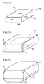
- Fig. 1A is a perspective view showing an initial single-crystalline diamond base material having an upper surface of a square ⁇ 100 ⁇ plane and side surfaces of ⁇ 100 ⁇ planes employed in each Example of the present invention
- Fig. 1B is a perspective view showing a shape of the single-crystalline diamond base material shown in Fig. 1A in an intermediate growth stage during prescribed vapor deposition
- Fig. 1C is a perspective view showing a shape of the single-crystalline diamond base material with upper ends of inclined surfaces growing from lower ends of the side surfaces reaching the vertical position of the upper major surface of the initial single-crystalline diamond base material;
- Fig. 2A is a perspective view showing a shape of the single-crystalline diamond base material shown in Fig. 1C after removing a portion between a lower surface and the upper ends of the inclined surfaces by polishing
- Fig. 2B is a perspective view showing a shape of the single-crystalline diamond base material shown in Fig. 2A after removing a portion between an upper surface and depressed parts on four upper corners by polishing
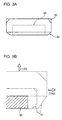
- Fig. 2C is a plan view showing positions for cutting the single-crystalline diamond base material formed through the step shown in Fig. 2B;
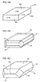
- Fig. 3A illustrates the single-crystalline diamond base material in the intermediate growth stage shown in Fig. 1B as viewed from a side surface
- Fig. 3B is a model diagram for illustrating the change of the shape of the single-crystalline diamond base material from the state shown in Fig. 1B to that shown in Fig. 1C during the growth process as viewed from the side surface;
- Fig. 4A is a plan view of the initial single-crystalline diamond base material shown in Fig. 1A
- Fig. 4B is a plan view of the single-crystalline diamond base material in the vapor deposition stage shown in Fig. 1B
- Fig. 4C is a plan view showing the single-crystalline diamond base material in the stage before the cutting step shown in Fig. 2C;
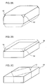
- Fig. 5A is a perspective view showing an initial single-crystalline diamond base material having an upper surface of a square ⁇ 100 ⁇ plane and side surfaces of ⁇ 110 ⁇ planes employed in each Example of the present invention
- Fig. 5B is a perspective view showing a shape of the single-crystalline diamond base material shown in Fig. 5A in an intermediate growth stage during prescribed vapor deposition
- Fig. 5C is a perspective view showing a shape of the single-crystalline diamond base material in a stage when intersection lines of pairs of inclined surfaces oppositely growing from upper and lower ends of the side surfaces form edge lines;
- Fig. 6A is a perspective view showing a shape of the single-crystalline diamond base material after removing a portion between an upper surface of the single-crystalline diamond base material shown in Fig. 5C and a plane including the edge lines formed by the pairs of intersection lines by polishing
- Fig. 6B is a perspective view showing a shape of the single-crystalline diamond base material shown in Fig. 6A after performing prescribed vapor deposition from a growth start surface defined by the upper surface of the single-crystalline diamond base material
- Fig. 6C is a perspective view showing a shape of the single-crystalline diamond base material after removing a portion between a lower surface formed through the step shown in Fig. 6B and the growth start surface by polishing, with cut positions in a subsequent cut-out step;
- Fig. 7A illustrates the single-crystalline diamond base material in the intermediate growth stage shown in Fig. 5B as viewed from a side surface
- Fig. 7B is a model diagram for illustrating the change of the shape of the single-crystalline diamond base material from the state shown in Fig. 5B to that shown in Fig. 5C during the growth process as viewed from the side surface;
- Fig. 8A is a plan view of the initial single-crystalline diamond base material shown in Fig. 5A
- Fig. 8B is a plan view of the single-crystalline diamond base material in the vapor deposition stage shown in Fig. 5B
- Fig. 8C is a plan view of the single-crystalline diamond base material before the cut-out step shown in Fig. 6C;
- Figs. 9A to 9C are plan views for illustrating preferable ranges of growth thicknesses of single-crystalline diamond toward side surfaces of base materials in stages of cutting the base materials, and among these figures, Fig. 9A is a plan view in case of cutting the base material along cut lines 12 forming a square when the growth thickness toward a ⁇ 100 ⁇ plane in a ⁇ 100> direction is about 22 % of the initial length of each side of the base material for cutting out diamond in the form of a square pole, Fig.
- FIG. 9B is a plan view in case of cutting the base material along cut lines 12 forming a square on corner portions when the growth thickness toward a ⁇ 100 ⁇ plane in a ⁇ 100> direction is about 22 % of the initial length of each side of the base material similarly to the case shown in Fig. 9A for cutting out diamond in the form of an octagonal pole
- Fig. 9C is a plan view in case of cutting the base material along cut lines 12 forming a square when the vapor deposition thickness toward a ⁇ 100 ⁇ plane in a ⁇ 100> direction is about 50 % of the initial length of each side of the base material for cutting out diamond in the form of a square pole;
- Fig. 10 is a model diagram showing a microwave CVD apparatus employed for an experiment in Example 1 of the present invention.
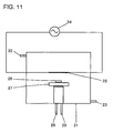
- Fig. 11 is a model diagram showing a thermal filament CVD apparatus for diamond vapor-phase synthesis employed for an experiment in Example 2 of the present invention.
- Fig. 10 is a model diagram showing a microwave CVD apparatus for diamond vapor-phase synthesis employed for an experiment in Example 1 of the present invention.
- a microwave generation part consisting of a microwave power source 4, an isolator, tuners 5 and the like generates microwaves, which are directed to a plunger 10 through a waveguide 6.
- the waveguide 6 is provided on its intermediate position with a silica tube 7 serving as a reaction vessel, which is provided with a source gas inlet port 9 and an outlet port 8 on its upper and lower portions respectively.
- a base material holder 1 is arranged on a position of the silica tube 7 intersecting with the waveguide 6, so that a base material 2 is set on this base material holder 1.
- a base material (hereinafter referred to as a prime base material) 50 shown in Figs. 1A and 4A is prepared from single-crystalline diamond of at least 0.5 mm in thickness having an upper surface 50a of a square ⁇ 100 ⁇ plane and side surfaces 50b and 50c of ⁇ 100 ⁇ planes and set on the base material holder 1, which is made of molybdenum, of the microwave CVD apparatus for homoepitaxially growing diamond under a ⁇ 100> preferential orientation growth condition at a growth rate ratio of about 3 0.5 with methane-hydrogen mixed gas having methane concentration of 10 ⁇ 0.5 % while maintaining the pressure in the reaction vessel 7 at 18665 ⁇ 667 Pa (140 ⁇ 5 Torr) and the temperature of the prime base material 50 at 1000 ⁇ 10°C.
- diamond grows as shown in Figs. 1B, 3A and 4B so that inclined surfaces 51 appear from lower portions of the side surfaces 50b and 50c of the prime base material 50 while abnormal growing parts 11 (see Fig. 4B) and depressed parts 52 appear on four corners and upper corner portions of an upper surface respectively.
- the diamond further grows with no abnormal growth on extensions of the ⁇ 100 ⁇ side surfaces 50b and 50c as shown in Fig. 1C, so that an upper end of each inclined surface 51 reaches a position shown by a broken line in Fig. 3B, i.e., the position of the upper major surface 50a of the prime base material 50.
- a broken line in Fig. 3B i.e., the position of the upper major surface 50a of the prime base material 50.
- the portion between a lower surface and the upper ends of the inclined surfaces 51 shown by broken lines in Fig. 2A is removed by polishing, and thereafter the portion shown by broken lines in Fig.
- a diamond substrate 53 which is in the form of a rectangular parallelepiped including the abnormal growing parts 11, as shown in Figs. 2C and 4C.
- This substrate 53 is cut along cut lines 12 shown in Figs. 2C and 4C with a YAG laser beam, thereby forming a flat single-crystalline diamond substrate (prime base material) 60 having an upper surface 60a consisting of a square ⁇ 100 ⁇ plane and four side surfaces 60b and 60c consisting of ⁇ 110 ⁇ planes, as shown in Figs. 5A and 8A.
- diamond is grown under a ⁇ 110> preferential orientation growth condition at a growth rate ratio of 0.5 x 3 0.5 with methane-hydrogen mixed gas having methane concentration of 3 ⁇ 0.5 % while maintaining the pressure in the reaction vessel 7 at 18665 ⁇ 667 Pa (140 ⁇ 5 Torr) and the temperature of the prime base material 60 at 1050 ⁇ 10°C, whereby the diamond grows as shown in Figs. 5B and 7A.
- inclines surfaces 61 and 62 appear as shown in Figs. 5B and 8B from upper and lower ends of the four side surfaces 60b and 60c of the prime base material 60 shown in Figs. 5A and 8A. While abnormal growing parts 11 appear on four corners of the prime base material 60, the diamond grows with no abnormal growth on extensions of the ⁇ 110 ⁇ side surfaces 60b and 60c.
- the substrate 64 located under the single-crystalline diamond layer 65 is removed by polishing from a lower surface, to obtain the flat single-crystalline diamond layer 65 including the abnormal growing parts 11 on four corners as shown in Figs. 6C and 8C.
- This single-crystalline diamond layer 65 is cut with a YAG laser beam along cut lines 12 shown in Fig. 6C, thereby forming single-crystalline diamond having an upper surface 50a and four side surfaces 50b and 50c all consisting of ⁇ 100 ⁇ planes and including no abnormal growing parts as shown in Fig. 1A.
- Flat single-crystalline diamond having a large area can be obtained by repeating the aforementioned steps.
- the object of the present invention can also be attained by employing a ⁇ 111> preferential orientation growth condition for most increasing the growth rate in ⁇ 111> directions in place of the ⁇ 110> preferential orientation growth condition, for the following reason:
- isolated grains of diamond formed by homoepitaxy from points are generally formed by two types of planes, i.e., ⁇ 100 ⁇ and ⁇ 111 ⁇ planes. This is because the diamond mainly grows toward the ⁇ 100 ⁇ and ⁇ 111 ⁇ planes in ⁇ 100> and ⁇ 111> directions while relatively hardly growing toward the remaining planes.
- the growth rate ratio serving as an index specifying each orientation growth direction is defined as the ratio of the vapor deposition rate V ⁇ 100> in the ⁇ 100> direction to the vapor deposition rate V ⁇ 111> in the ⁇ 111> direction, therefore, it is known that the growth rates toward the remaining low-index planes are decided by the large-small relation between the growth rates in the ⁇ 100> and ⁇ 111> directions.
- the growth rate ratio is 0.5 x 3 0.5 and the vapor deposition rate in the ⁇ 111> direction is higher than that in the ⁇ 100> direction, whereby the growth of the diamond is remarkably influenced by the vapor deposition in the ⁇ 111> direction. Therefore, the diamond grows into the shape shown in Fig. 7A after vapor deposition, and the thickness of each ⁇ 110 ⁇ plane is gradually reduced as shown in Fig. 7B, to reduce the thickness of each region causing no abnormal growth.
- the ⁇ 111> preferential orientation growth condition is applied to the prime base material 60 shown in Fig.
- the object of the present invention can also be attained by applying the ⁇ 111> orientation growth condition dissimilarly to the ⁇ 110> orientation growth condition for most increasing the growth rate toward the side surfaces in case of homoepitaxially growing diamond on a prime base material having a major surface of a ⁇ 100 ⁇ plane and side surfaces of ⁇ 110 ⁇ planes.
- a method of obtaining single-crystalline diamond having the largest area in the cutting step with the YAG laser beam in this Example is now described.
- the step of cutting the prime base material 50 or 60 with the YAG laser beam along the cut lines 12 described with reference to Figs. 2C and 4C or 6C and 8C is carried out when single-crystalline diamond grows on the side surfaces 50b and 50c or 60b and 60c of the single-crystalline diamond base material 50 or 60 in a thickness of not more than 50 % of the initial length of each side.
- the prime base material 50 or 60 is cut when the single-crystalline diamond grows on the side surfaces 50b and 50c or 60b and 60c in a thickness exceeding 50 % of the initial length of each side, portions including no abnormal growth are removed in a large amount against the object of the present invention for quickly forming single-crystalline diamond having a larger area.
- Figs. 9A to 9C illustrate preferable ranges of growth thicknesses of single-crystalline diamond toward side surfaces of base materials in stages of cutting the base materials.
- the area s1 of a triangle formed on each corner of diamond which is cut out from the initial base material is substantially identical to the area s2 of each growing part remaining as a new corner part after cutting, whereby the plane area of the cut base material is substantially equal to that of the base material in consequence. If the base material is cut along the ⁇ 110 ⁇ planes on four corners into the form of a square pole while removing the abnormal growing parts when the growth thickness toward the ⁇ 100 ⁇ planes in the ⁇ 100> directions is not in excess of about 22 % of the initial length of each side of the base material, therefore, the plane area of the cut base material is merely identical to or smaller than that of the initial base material.
- the diamond is preferably cut out by cutting the base material along the ⁇ 110 ⁇ planes on the four corners when the growth thickness toward the ⁇ 100 ⁇ planes in the ⁇ 100> directions is not more than 50 % of the initial length of each side of the base material, and it is most optimum to cut out the diamond when the growth thickness is 50 %.
- Example 2 of the present invention for vapor-phase synthesizing single-crystalline diamond with application of a thermal filament method is now described.
- Fig. 11 is a model diagram showing a thermal filament CVD apparatus for diamond vapor-phase synthesis employed for an experiment.
- a reaction vessel 21 is provided with an inlet port 22 and an outlet port 23 for source gas.
- a tungsten filament 25 is arranged in the reaction vessel 21, and an ac power source 24 feeds a current for red-heating the tungsten filament 25.
- a base material holder 27 of molybdenum is arranged under the tungsten filament 25, for receiving a single-crystalline diamond base material 26.
- An inlet port 28 and an outlet port 29 for cooling water are provided for supplying cooling water to a lower portion of the base material holder 27 which is heated to a high temperature by the red-heated tungsten filament 25.
- the single-crystalline diamond base material 26 is prepared from the single-crystalline diamond base material (prime base material) 50 of at least 0.5 mm in thickness having the upper surface 50a of a square ⁇ 100 ⁇ plane and the side surfaces 50b and 50c of ⁇ 100 ⁇ planes as shown in Figs.
- the diamond further grows with no abnormal growth on extensions of the ⁇ 100 ⁇ side surfaces 50b and 50c as shown in Fig. 1C, so that an upper end of each inclined surface 51 reaches the position shown by the broken line in Fig. 3B, i.e., the position of the upper major surface 50a of the prime base material 50.
- the portion between a lower surface and the upper ends of the inclined surfaces 51 shown by broken lines in Fig. 2A is removed by polishing, and thereafter the portion shown by broken lines in Fig.
- a diamond substrate 53 which is in the form of a rectangular parallelepiped including the abnormal growing parts 11, as shown in Figs. 2C and 4C.
- This substrate 53 is cut along cut lines 12 shown in Figs. 2C and 4C with a YAG laser beam, thereby forming a flat single-crystalline diamond substrate (prime base material) 60 having an upper surface 60a consisting of a square ⁇ 100 ⁇ plane and four side surfaces 60b and 60c consisting of ⁇ 110 ⁇ planes, as shown in Figs. 5A and 8A.
- diamond is grown under a ⁇ 110> preferential orientation growth condition at a growth rate ratio of 0.5 x 3 0.5 with methane-hydrogen mixed gas having methane concentration of 1.2 % while maintaining the pressure in the reaction vessel 27 at 13332 Pa (100 Torr) and the temperature of the prime base material 60 at 850°C, whereby diamond grows as shown in Figs. 5B and 7A.
- inclines surfaces 61 and 62 appear as shown in Figs. 5B and 8B from upper and lower ends of the four side surfaces 60b and 60c of the prime base material 60 shown in Figs. 5A and 8A.
- abnormal growing parts 11 appear on four corners of the prime base material 60, the diamond grows with no abnormal growth on extensions of the ⁇ 110 ⁇ side surfaces 60b and 60c.
- the substrate 64 located under the single-crystalline diamond layer 65 is removed by polishing from a lower surface, to obtain the flat single-crystalline diamond layer 65 including the abnormal growing parts 11 on four corners as shown in Figs. 6C and 8C.
- This single-crystalline diamond layer 65 is cut with a YAG laser beam along cut lines 12 shown in Fig. 6C, thereby forming single-crystalline diamond having an upper surface 50a and four side surfaces 50b and 50c all consisting of ⁇ 100 ⁇ planes and including no abnormal growing parts as shown in Fig. 1A.
- Flat single-crystalline diamond having a large area can be obtained by repeating the aforementioned steps.
- the object of the present invention can be attained by applying the ⁇ 111> preferential orientation growth condition dissimilarly to the ⁇ 110> preferential orientation growth condition for most increasing the growth rate toward the side surfaces in case of homoepitaxially growing diamond on a prime base material having a major surface of a ⁇ 100 ⁇ plane and side surfaces of ⁇ 110 ⁇ planes similarly to Example 1, as a matter of course.
- the surfaces grown by vapor deposition and the cut planes in the cutting step are formed by ⁇ 100 ⁇ , ⁇ 110 ⁇ and ⁇ 111 ⁇ planes in each Example, the surfaces may not necessarily coincide with such plane orientations but the object of the present invention can be attained when the plane orientations of these surfaces are within the range included in the aforementioned definition of the low-index planes.
Landscapes
- Chemical & Material Sciences (AREA)
- Engineering & Computer Science (AREA)
- Crystallography & Structural Chemistry (AREA)
- Materials Engineering (AREA)
- Metallurgy (AREA)
- Organic Chemistry (AREA)
- Chemical Kinetics & Catalysis (AREA)
- General Chemical & Material Sciences (AREA)
- Crystals, And After-Treatments Of Crystals (AREA)
- Chemical Vapour Deposition (AREA)
Applications Claiming Priority (6)
| Application Number | Priority Date | Filing Date | Title |
|---|---|---|---|
| JP10161397 | 1997-04-18 | ||
| JP10161397 | 1997-04-18 | ||
| JP101613/97 | 1997-04-18 | ||
| JP04332598A JP4032482B2 (ja) | 1997-04-18 | 1998-02-25 | 単結晶ダイヤモンドの製造方法 |
| JP43325/98 | 1998-02-25 | ||
| JP4332598 | 1998-02-25 |
Publications (2)
| Publication Number | Publication Date |
|---|---|
| EP0879904A1 EP0879904A1 (en) | 1998-11-25 |
| EP0879904B1 true EP0879904B1 (en) | 2001-10-17 |
Family
ID=26383082
Family Applications (1)
| Application Number | Title | Priority Date | Filing Date |
|---|---|---|---|
| EP98302982A Expired - Lifetime EP0879904B1 (en) | 1997-04-18 | 1998-04-17 | Method and apparatus for producing single-crystalline diamond |
Country Status (4)
| Country | Link |
|---|---|
| US (1) | US6096129A (https=) |
| EP (1) | EP0879904B1 (https=) |
| JP (1) | JP4032482B2 (https=) |
| DE (1) | DE69802037T2 (https=) |
Cited By (1)
| Publication number | Priority date | Publication date | Assignee | Title |
|---|---|---|---|---|
| CN110789011A (zh) * | 2019-11-07 | 2020-02-14 | 北京昌日新能源科技有限公司 | 一种新型光伏用直角单晶硅片及其制造方法 |
Families Citing this family (41)
| Publication number | Priority date | Publication date | Assignee | Title |
|---|---|---|---|---|
| US6858080B2 (en) | 1998-05-15 | 2005-02-22 | Apollo Diamond, Inc. | Tunable CVD diamond structures |
| US8591856B2 (en) | 1998-05-15 | 2013-11-26 | SCIO Diamond Technology Corporation | Single crystal diamond electrochemical electrode |
| US6582513B1 (en) | 1998-05-15 | 2003-06-24 | Apollo Diamond, Inc. | System and method for producing synthetic diamond |
| CZ302228B6 (cs) | 2000-06-15 | 2011-01-05 | Element Six (Pty) Ltd | Monokrystalická diamantová vrstva pripravená chemickým vylucováním z plynné fáze |
| EP1290251B8 (en) * | 2000-06-15 | 2006-02-01 | Element Six (PTY) Ltd | Thick single crystal diamond layer method for making it and gemstones produced from the layer |
| AU2001281404B2 (en) * | 2001-08-08 | 2008-07-03 | Apollo Diamond, Inc. | System and method for producing synthetic diamond |
| GB0130004D0 (en) | 2001-12-14 | 2002-02-06 | Diamanx Products Ltd | Coloured diamond |
| GB0130005D0 (en) * | 2001-12-14 | 2002-02-06 | Diamanx Products Ltd | Boron doped diamond |
| US7060130B2 (en) * | 2002-08-27 | 2006-06-13 | Board Of Trustees Of Michigan State University | Heteroepitaxial diamond and diamond nuclei precursors |
| RU2328563C2 (ru) * | 2002-09-06 | 2008-07-10 | Элемент Сикс Лимитед | Цветные алмазы |
| GB0221949D0 (en) * | 2002-09-20 | 2002-10-30 | Diamanx Products Ltd | Single crystal diamond |
| GB0227261D0 (en) | 2002-11-21 | 2002-12-31 | Element Six Ltd | Optical quality diamond material |
| GB0303860D0 (en) | 2003-02-19 | 2003-03-26 | Element Six Ltd | CVD diamond in wear applications |
| WO2005061400A1 (en) | 2003-12-12 | 2005-07-07 | Element Six Limited | Method of incorporating a mark in cvd diamond |
| KR101240785B1 (ko) | 2003-12-12 | 2013-03-07 | 엘리멘트 식스 리미티드 | 화학적 증착 다이아몬드에 마크를 통합시키는 방법 |
| JP5163920B2 (ja) * | 2005-03-28 | 2013-03-13 | 住友電気工業株式会社 | ダイヤモンド単結晶基板の製造方法及びダイヤモンド単結晶基板 |
| JP5002982B2 (ja) * | 2005-04-15 | 2012-08-15 | 住友電気工業株式会社 | 単結晶ダイヤモンドの製造方法 |
| JP5594613B2 (ja) * | 2005-04-15 | 2014-09-24 | 住友電気工業株式会社 | 単結晶ダイヤモンドおよびその製造方法 |
| JP4613314B2 (ja) * | 2005-05-26 | 2011-01-19 | 独立行政法人産業技術総合研究所 | 単結晶の製造方法 |
| AU2006260656A1 (en) | 2005-06-22 | 2006-12-28 | Element Six Limited | High colour diamond layer |
| WO2007029269A1 (en) * | 2005-09-05 | 2007-03-15 | Rajneesh Bhandari | Synthesis of large homoepitaxial monocrystalline diamond |
| JP4873368B2 (ja) * | 2007-01-24 | 2012-02-08 | 住友電気工業株式会社 | ダイヤモンド基板 |
| GB0704516D0 (en) * | 2007-03-08 | 2007-04-18 | Element Six Ltd | Diamond |
| US8342164B2 (en) * | 2008-05-09 | 2013-01-01 | SCIO Diamond Technology Corporation | Gemstone production from CVD diamond plate |
| GB0813491D0 (en) | 2008-07-23 | 2008-08-27 | Element Six Ltd | Diamond Material |
| GB0813490D0 (en) | 2008-07-23 | 2008-08-27 | Element Six Ltd | Solid state material |
| GB0900771D0 (en) | 2009-01-16 | 2009-03-04 | Element Six Ltd | Diamond |
| US9157170B2 (en) | 2009-12-21 | 2015-10-13 | Element Six Technologies Limited | Single crystal diamond material |
| GB2476306B (en) * | 2009-12-21 | 2012-07-11 | Element Six Ltd | Single crystal diamond material |
| GB201000768D0 (en) | 2010-01-18 | 2010-03-03 | Element Six Ltd | CVD single crystal diamond material |
| US9017633B2 (en) * | 2010-01-18 | 2015-04-28 | Element Six Technologies Limited | CVD single crystal diamond material |
| JP5831796B2 (ja) * | 2011-09-06 | 2015-12-09 | 住友電気工業株式会社 | ダイヤモンド複合体およびそれから分離した単結晶ダイヤモンド、及びダイヤモンド複合体の製造方法 |
| US20150191846A1 (en) * | 2012-08-17 | 2015-07-09 | Gtat Corporation | System and method of growing silicon ingots from seeds in a crucible and manufacture of seeds used therein |
| EP3054036B1 (en) * | 2013-09-30 | 2021-03-03 | Adamant Namiki Precision Jewel Co., Ltd. | Diamond substrate manufacturing method |
| CN108908762A (zh) * | 2018-06-15 | 2018-11-30 | 西安碳星半导体科技有限公司 | Cvd生长宝石级厚单晶金刚石切割方法 |
| CN111850682B (zh) * | 2020-07-23 | 2021-09-07 | 太原理工大学 | 同时扩大单晶金刚石籽晶尺寸及数量的方法 |
| CN111690981B (zh) * | 2020-07-23 | 2021-08-03 | 太原理工大学 | 一种扩大单晶金刚石籽晶尺寸及数量的方法 |
| EP4269004B1 (en) * | 2020-12-24 | 2024-10-23 | Sumitomo Electric Hardmetal Corp. | Method for producing diamond tool intermediate and method for determining single crystal diamond |
| GB2609023A (en) * | 2021-07-18 | 2023-01-25 | Lusix Ltd | Growing of diamonds |
| CN114232091B (zh) * | 2021-12-27 | 2024-05-10 | 苏州贝莱克金刚石科技有限公司 | 大尺寸单晶金刚石及其制备方法 |
| GB202305972D0 (en) | 2023-04-24 | 2023-06-07 | Element Six Tech Ltd | Method of manufacturing single crystal diamonds |
Family Cites Families (5)
| Publication number | Priority date | Publication date | Assignee | Title |
|---|---|---|---|---|
| JPH01103993A (ja) * | 1987-10-16 | 1989-04-21 | Sumitomo Electric Ind Ltd | ダイヤモンド単結晶成長方法 |
| JPH01103994A (ja) * | 1987-10-16 | 1989-04-21 | Sumitomo Electric Ind Ltd | ダイヤモンドの単結晶成長方法 |
| US5127983A (en) * | 1989-05-22 | 1992-07-07 | Sumitomo Electric Industries, Ltd. | Method of producing single crystal of high-pressure phase material |
| US5474021A (en) * | 1992-09-24 | 1995-12-12 | Sumitomo Electric Industries, Ltd. | Epitaxial growth of diamond from vapor phase |
| DE69417627T2 (de) * | 1993-01-14 | 1999-09-09 | Sumitomo Electric Industries | Verfahren zur dampfphasendiamantsynthese |
-
1998
- 1998-02-25 JP JP04332598A patent/JP4032482B2/ja not_active Expired - Lifetime
- 1998-04-15 US US09/060,555 patent/US6096129A/en not_active Expired - Lifetime
- 1998-04-17 EP EP98302982A patent/EP0879904B1/en not_active Expired - Lifetime
- 1998-04-17 DE DE69802037T patent/DE69802037T2/de not_active Expired - Lifetime
Non-Patent Citations (1)
| Title |
|---|
| T. INUZUKA AND A. SAWABE: "Growth of Diamond Thin Films from the Vapor Phase and Their Charaterization", APPLIED PHYSICS, vol. 55, no. 7, 1986 - 1986, pages 640 - 653 * |
Cited By (1)
| Publication number | Priority date | Publication date | Assignee | Title |
|---|---|---|---|---|
| CN110789011A (zh) * | 2019-11-07 | 2020-02-14 | 北京昌日新能源科技有限公司 | 一种新型光伏用直角单晶硅片及其制造方法 |
Also Published As
| Publication number | Publication date |
|---|---|
| JP4032482B2 (ja) | 2008-01-16 |
| DE69802037T2 (de) | 2002-03-14 |
| JPH111392A (ja) | 1999-01-06 |
| DE69802037D1 (de) | 2001-11-22 |
| EP0879904A1 (en) | 1998-11-25 |
| US6096129A (en) | 2000-08-01 |
Similar Documents
| Publication | Publication Date | Title |
|---|---|---|
| EP0879904B1 (en) | Method and apparatus for producing single-crystalline diamond | |
| US7736435B2 (en) | Method of producing single crystal | |
| US5474021A (en) | Epitaxial growth of diamond from vapor phase | |
| JP2654232B2 (ja) | 高圧相物質単結晶の製造方法 | |
| KR0170536B1 (ko) | 웨이퍼 및 그 제조방법 | |
| EP0612868A1 (en) | Single crystal diamond and process for producing the same | |
| EP1712661B2 (en) | Single crystalline diamond and producing method thereof | |
| US20250059677A1 (en) | Method of Growing Single Crystal Diamond Assisted by Polycrystalline Diamond Growth | |
| JPH0748198A (ja) | ダイヤモンドの合成法 | |
| JP3728464B2 (ja) | 単結晶ダイヤモンド膜気相合成用基板の製造方法 | |
| WO1989011897A1 (en) | Silicon dioxide films on diamond | |
| JPH06107494A (ja) | ダイヤモンドの気相成長法 | |
| JP6887893B2 (ja) | 単結晶ダイヤモンドの製造方法、単結晶ダイヤモンド複合体および単結晶ダイヤモンド基板 | |
| JP3296148B2 (ja) | ウエハ−及びその製造方法 | |
| Findeling-Dufour et al. | Study for fabricating large area diamond single-crystal layers | |
| US5198070A (en) | Joining diamond bodies | |
| JPH0687691A (ja) | ダイヤモンドの製造方法およびダイヤモンドの製造方法に使用するダイヤモンド単結晶基材 | |
| CN117448951B (zh) | 基于边缘晶向处理减少金刚石晶体生长相互干涉的方法 | |
| JPH06227895A (ja) | ダイヤモンドの合成法 | |
| JP7487702B2 (ja) | 単結晶ダイヤモンド基板の製造方法 | |
| CN117448950A (zh) | 基于边缘激光蚀刻处理减少金刚石晶体生长相互干涉的方法 | |
| EP0492160A1 (en) | Symmetric CVD diamond articles and method of their preparation | |
| JPH05201794A (ja) | ダイヤモンド半導体製造方法 | |
| JPH0672797A (ja) | 高圧相物質の合成方法 | |
| JPH05201795A (ja) | 単結晶粒製造方法 |
Legal Events
| Date | Code | Title | Description |
|---|---|---|---|
| PUAI | Public reference made under article 153(3) epc to a published international application that has entered the european phase |
Free format text: ORIGINAL CODE: 0009012 |
|
| AK | Designated contracting states |
Kind code of ref document: A1 Designated state(s): DE FR GB |
|
| AX | Request for extension of the european patent |
Free format text: AL;LT;LV;MK;RO;SI |
|
| 17P | Request for examination filed |
Effective date: 19990525 |
|
| AKX | Designation fees paid |
Free format text: DE FR GB |
|
| 17Q | First examination report despatched |
Effective date: 19991025 |
|
| GRAG | Despatch of communication of intention to grant |
Free format text: ORIGINAL CODE: EPIDOS AGRA |
|
| GRAG | Despatch of communication of intention to grant |
Free format text: ORIGINAL CODE: EPIDOS AGRA |
|
| GRAG | Despatch of communication of intention to grant |
Free format text: ORIGINAL CODE: EPIDOS AGRA |
|
| GRAH | Despatch of communication of intention to grant a patent |
Free format text: ORIGINAL CODE: EPIDOS IGRA |
|
| GRAH | Despatch of communication of intention to grant a patent |
Free format text: ORIGINAL CODE: EPIDOS IGRA |
|
| GRAA | (expected) grant |
Free format text: ORIGINAL CODE: 0009210 |
|
| AK | Designated contracting states |
Kind code of ref document: B1 Designated state(s): DE FR GB |
|
| REF | Corresponds to: |
Ref document number: 69802037 Country of ref document: DE Date of ref document: 20011122 |
|
| REG | Reference to a national code |
Ref country code: GB Ref legal event code: IF02 |
|
| ET | Fr: translation filed | ||
| PLBE | No opposition filed within time limit |
Free format text: ORIGINAL CODE: 0009261 |
|
| STAA | Information on the status of an ep patent application or granted ep patent |
Free format text: STATUS: NO OPPOSITION FILED WITHIN TIME LIMIT |
|
| 26N | No opposition filed | ||
| PGFP | Annual fee paid to national office [announced via postgrant information from national office to epo] |
Ref country code: FR Payment date: 20120504 Year of fee payment: 15 |
|
| REG | Reference to a national code |
Ref country code: FR Ref legal event code: ST Effective date: 20131231 |
|
| PG25 | Lapsed in a contracting state [announced via postgrant information from national office to epo] |
Ref country code: FR Free format text: LAPSE BECAUSE OF NON-PAYMENT OF DUE FEES Effective date: 20130430 |
|
| PGFP | Annual fee paid to national office [announced via postgrant information from national office to epo] |
Ref country code: DE Payment date: 20160412 Year of fee payment: 19 Ref country code: GB Payment date: 20160413 Year of fee payment: 19 |
|
| REG | Reference to a national code |
Ref country code: DE Ref legal event code: R119 Ref document number: 69802037 Country of ref document: DE |
|
| GBPC | Gb: european patent ceased through non-payment of renewal fee |
Effective date: 20170417 |
|
| PG25 | Lapsed in a contracting state [announced via postgrant information from national office to epo] |
Ref country code: DE Free format text: LAPSE BECAUSE OF NON-PAYMENT OF DUE FEES Effective date: 20171103 |
|
| PG25 | Lapsed in a contracting state [announced via postgrant information from national office to epo] |
Ref country code: GB Free format text: LAPSE BECAUSE OF NON-PAYMENT OF DUE FEES Effective date: 20170417 |