EP0856199B1 - Polymeres höcker-matrix-gehäuse - Google Patents
Polymeres höcker-matrix-gehäuse Download PDFInfo
- Publication number
- EP0856199B1 EP0856199B1 EP96934620A EP96934620A EP0856199B1 EP 0856199 B1 EP0856199 B1 EP 0856199B1 EP 96934620 A EP96934620 A EP 96934620A EP 96934620 A EP96934620 A EP 96934620A EP 0856199 B1 EP0856199 B1 EP 0856199B1
- Authority
- EP
- European Patent Office
- Prior art keywords
- polymer
- grid array
- substrate
- heat sink
- stud grid
- Prior art date
- Legal status (The legal status is an assumption and is not a legal conclusion. Google has not performed a legal analysis and makes no representation as to the accuracy of the status listed.)
- Expired - Lifetime
Links
Images
Classifications
-
- H—ELECTRICITY
- H01—ELECTRIC ELEMENTS
- H01L—SEMICONDUCTOR DEVICES NOT COVERED BY CLASS H10
- H01L23/00—Details of semiconductor or other solid state devices
- H01L23/12—Mountings, e.g. non-detachable insulating substrates
- H01L23/13—Mountings, e.g. non-detachable insulating substrates characterised by the shape
-
- H—ELECTRICITY
- H01—ELECTRIC ELEMENTS
- H01L—SEMICONDUCTOR DEVICES NOT COVERED BY CLASS H10
- H01L23/00—Details of semiconductor or other solid state devices
- H01L23/34—Arrangements for cooling, heating, ventilating or temperature compensation ; Temperature sensing arrangements
- H01L23/42—Fillings or auxiliary members in containers or encapsulations selected or arranged to facilitate heating or cooling
- H01L23/433—Auxiliary members in containers characterised by their shape, e.g. pistons
- H01L23/4334—Auxiliary members in encapsulations
-
- H—ELECTRICITY
- H01—ELECTRIC ELEMENTS
- H01L—SEMICONDUCTOR DEVICES NOT COVERED BY CLASS H10
- H01L2224/00—Indexing scheme for arrangements for connecting or disconnecting semiconductor or solid-state bodies and methods related thereto as covered by H01L24/00
- H01L2224/01—Means for bonding being attached to, or being formed on, the surface to be connected, e.g. chip-to-package, die-attach, "first-level" interconnects; Manufacturing methods related thereto
- H01L2224/42—Wire connectors; Manufacturing methods related thereto
- H01L2224/47—Structure, shape, material or disposition of the wire connectors after the connecting process
- H01L2224/48—Structure, shape, material or disposition of the wire connectors after the connecting process of an individual wire connector
- H01L2224/481—Disposition
- H01L2224/48151—Connecting between a semiconductor or solid-state body and an item not being a semiconductor or solid-state body, e.g. chip-to-substrate, chip-to-passive
- H01L2224/48221—Connecting between a semiconductor or solid-state body and an item not being a semiconductor or solid-state body, e.g. chip-to-substrate, chip-to-passive the body and the item being stacked
- H01L2224/48225—Connecting between a semiconductor or solid-state body and an item not being a semiconductor or solid-state body, e.g. chip-to-substrate, chip-to-passive the body and the item being stacked the item being non-metallic, e.g. insulating substrate with or without metallisation
- H01L2224/48227—Connecting between a semiconductor or solid-state body and an item not being a semiconductor or solid-state body, e.g. chip-to-substrate, chip-to-passive the body and the item being stacked the item being non-metallic, e.g. insulating substrate with or without metallisation connecting the wire to a bond pad of the item
-
- H—ELECTRICITY
- H01—ELECTRIC ELEMENTS
- H01L—SEMICONDUCTOR DEVICES NOT COVERED BY CLASS H10
- H01L24/00—Arrangements for connecting or disconnecting semiconductor or solid-state bodies; Methods or apparatus related thereto
- H01L24/01—Means for bonding being attached to, or being formed on, the surface to be connected, e.g. chip-to-package, die-attach, "first-level" interconnects; Manufacturing methods related thereto
- H01L24/42—Wire connectors; Manufacturing methods related thereto
- H01L24/47—Structure, shape, material or disposition of the wire connectors after the connecting process
- H01L24/48—Structure, shape, material or disposition of the wire connectors after the connecting process of an individual wire connector
-
- H—ELECTRICITY
- H01—ELECTRIC ELEMENTS
- H01L—SEMICONDUCTOR DEVICES NOT COVERED BY CLASS H10
- H01L2924/00—Indexing scheme for arrangements or methods for connecting or disconnecting semiconductor or solid-state bodies as covered by H01L24/00
- H01L2924/0001—Technical content checked by a classifier
- H01L2924/00014—Technical content checked by a classifier the subject-matter covered by the group, the symbol of which is combined with the symbol of this group, being disclosed without further technical details
-
- H—ELECTRICITY
- H01—ELECTRIC ELEMENTS
- H01L—SEMICONDUCTOR DEVICES NOT COVERED BY CLASS H10
- H01L2924/00—Indexing scheme for arrangements or methods for connecting or disconnecting semiconductor or solid-state bodies as covered by H01L24/00
- H01L2924/10—Details of semiconductor or other solid state devices to be connected
- H01L2924/11—Device type
- H01L2924/12—Passive devices, e.g. 2 terminal devices
- H01L2924/1204—Optical Diode
- H01L2924/12042—LASER
-
- H—ELECTRICITY
- H01—ELECTRIC ELEMENTS
- H01L—SEMICONDUCTOR DEVICES NOT COVERED BY CLASS H10
- H01L2924/00—Indexing scheme for arrangements or methods for connecting or disconnecting semiconductor or solid-state bodies as covered by H01L24/00
- H01L2924/10—Details of semiconductor or other solid state devices to be connected
- H01L2924/11—Device type
- H01L2924/14—Integrated circuits
-
- H—ELECTRICITY
- H01—ELECTRIC ELEMENTS
- H01L—SEMICONDUCTOR DEVICES NOT COVERED BY CLASS H10
- H01L2924/00—Indexing scheme for arrangements or methods for connecting or disconnecting semiconductor or solid-state bodies as covered by H01L24/00
- H01L2924/15—Details of package parts other than the semiconductor or other solid state devices to be connected
- H01L2924/151—Die mounting substrate
- H01L2924/1515—Shape
- H01L2924/15153—Shape the die mounting substrate comprising a recess for hosting the device
- H01L2924/15155—Shape the die mounting substrate comprising a recess for hosting the device the shape of the recess being other than a cuboid
- H01L2924/15157—Top view
-
- H—ELECTRICITY
- H01—ELECTRIC ELEMENTS
- H01L—SEMICONDUCTOR DEVICES NOT COVERED BY CLASS H10
- H01L2924/00—Indexing scheme for arrangements or methods for connecting or disconnecting semiconductor or solid-state bodies as covered by H01L24/00
- H01L2924/15—Details of package parts other than the semiconductor or other solid state devices to be connected
- H01L2924/151—Die mounting substrate
- H01L2924/153—Connection portion
- H01L2924/1531—Connection portion the connection portion being formed only on the surface of the substrate opposite to the die mounting surface
- H01L2924/15311—Connection portion the connection portion being formed only on the surface of the substrate opposite to the die mounting surface being a ball array, e.g. BGA
-
- H—ELECTRICITY
- H01—ELECTRIC ELEMENTS
- H01L—SEMICONDUCTOR DEVICES NOT COVERED BY CLASS H10
- H01L2924/00—Indexing scheme for arrangements or methods for connecting or disconnecting semiconductor or solid-state bodies as covered by H01L24/00
- H01L2924/15—Details of package parts other than the semiconductor or other solid state devices to be connected
- H01L2924/151—Die mounting substrate
- H01L2924/153—Connection portion
- H01L2924/1532—Connection portion the connection portion being formed on the die mounting surface of the substrate
-
- H—ELECTRICITY
- H01—ELECTRIC ELEMENTS
- H01L—SEMICONDUCTOR DEVICES NOT COVERED BY CLASS H10
- H01L2924/00—Indexing scheme for arrangements or methods for connecting or disconnecting semiconductor or solid-state bodies as covered by H01L24/00
- H01L2924/15—Details of package parts other than the semiconductor or other solid state devices to be connected
- H01L2924/161—Cap
- H01L2924/1615—Shape
- H01L2924/16195—Flat cap [not enclosing an internal cavity]
-
- H—ELECTRICITY
- H01—ELECTRIC ELEMENTS
- H01L—SEMICONDUCTOR DEVICES NOT COVERED BY CLASS H10
- H01L2924/00—Indexing scheme for arrangements or methods for connecting or disconnecting semiconductor or solid-state bodies as covered by H01L24/00
- H01L2924/15—Details of package parts other than the semiconductor or other solid state devices to be connected
- H01L2924/181—Encapsulation
-
- H—ELECTRICITY
- H01—ELECTRIC ELEMENTS
- H01L—SEMICONDUCTOR DEVICES NOT COVERED BY CLASS H10
- H01L2924/00—Indexing scheme for arrangements or methods for connecting or disconnecting semiconductor or solid-state bodies as covered by H01L24/00
- H01L2924/19—Details of hybrid assemblies other than the semiconductor or other solid state devices to be connected
- H01L2924/191—Disposition
- H01L2924/19101—Disposition of discrete passive components
- H01L2924/19107—Disposition of discrete passive components off-chip wires
-
- H—ELECTRICITY
- H01—ELECTRIC ELEMENTS
- H01L—SEMICONDUCTOR DEVICES NOT COVERED BY CLASS H10
- H01L2924/00—Indexing scheme for arrangements or methods for connecting or disconnecting semiconductor or solid-state bodies as covered by H01L24/00
- H01L2924/30—Technical effects
- H01L2924/301—Electrical effects
- H01L2924/3025—Electromagnetic shielding
Definitions
- Integrated circuits are getting more and more connections and are miniaturized more and more.
- the one at this increasing miniaturization expected difficulties with Solder paste application and assembly, should be due to new housing shapes be remedied, in particular single few or to highlight multi-chip modules in the Ball Grid Array Package are (DE-Z productronic 5, 1994, pages 54, 55).
- This Modules are based on a plated-through substrate which the chips for example via contact wires or are contacted by means of flip chip assembly.
- the substrate On the bottom the substrate is the Ball Grid Array (BGA), the often as a Solder Grid Array, Land Grid Array or Solder Bump array.
- the ball grid array includes solder bumps arranged flat on the underside of the substrate, which is a surface mount on the circuit boards or enable modules. Due to the flat arrangement of the Solder bumps can have large numbers of connections in a rough grid of, for example, 1.27 mm.
- MID M oulded I nterconnection D evices
- injection-molded parts are used with integrated conductor tracks instead of conventional printed circuits.
- High-quality thermoplastics that are suitable for injection molding three-dimensional substrates are the basis of this technology.
- Thermoplastics of this type are distinguished from conventional substrate materials for printed circuits by better mechanical, thermal, chemical, electrical and environmental properties.
- SIL S injection-molded parts with i ntegr faced L pus-trains
- the structuring is a layer applied to the molded parts metal layer, dispensing with the usual mask technique using a special laser patterning method.
- the housing support function takes on guides and snap connections at the same time, while the metallization layer also serves as an electromagnetic shield in addition to the wiring and connection function and ensures good heat dissipation. Further details on the production of three-dimensional injection molded parts with integrated conductor tracks can be found, for example, in DE-A-37 32 249 or EP-A-0 361 192.
- From US-A-5 081 520 is a method for attaching IC chips known on substrates, in which the substrates as injection molded parts with integrated bumps for fastening of the IC chips are manufactured. After metallizing a connection layer is applied to the bump so that the IC chips can be attached to the substrates, whereby the chip pads with the assigned metallizations the hump can be electrically connected.
- WO-A-89/00346 discloses a carrier arrangement for IC chips known in which the injection molded substrate on its Underside formed during injection molding bumps. On An IC chip is arranged on the upper side of the substrate Connections via bond wires with on the top of the substrate trained interconnects are connected.
- the manufacture can also of the external connections on the polymer bumps with minimal Effort together with the MID technology or the usual way of producing the conductor tracks become. Due to the laser fine structuring preferred in the SIL technique, can the external connections on the polymer bumps with high connection numbers in a very fine grid will be realized. It should also be emphasized that the Temperature expansion of the polymer bumps the temperature expansion of the substrate and the circuit board receiving the module corresponds. If mechanical stresses occur, so the polymer bumps enable through their elastic properties at least a partial compensation. Through the Dimensional stability of the external connections formed on the polymer bumps, can also provide security for repairs and replacements opposite the Ball Grid Arrays with theirs by Lothökker formed external connections can be increased significantly.
- the invention specified in claim 1 is based on the problem to create a polymer stud grid array where an improved dissipation of the heat loss is achieved.
- the invention is based on the knowledge that in the manufacture the substrates of polymer stud grid arrays Injection molding with little additional effort a heat sink partially embedded in the substrate material can. All that is required is an injection mold, in which the heat sink before the injection molding process can be positioned at a predetermined position. After Manufacturing the polymer stud grid array is a very then good dissipation of the heat loss on the heat sink arranged chips or one arranged on the heat-conducting body Wiring element guaranteed.
- the embodiment according to claim 2 enables a sunken Assembly of the chips or wiring elements in troughs injection molded substrates, the bottom of which by the heat sink is formed. This can result in an extremely small thickness of the resulting single, Few or multi-chip modules become.
- the sunken assembly also enables optimal protection of the chips or wiring elements.
- the embodiment according to claim 3 enables a particularly easy introduction of the heat-conducting body into the substrate material during injection molding.
- the disc shape favors the application of a chip or one of the heat-conducting body Wiring element.
- the training according to claim 4 also enables one different temperatures from low-stress composite Substrate and heat sink.
- a ceramic heat-conducting body can also be used be used successfully, here according to claim 8 in particular heat conducting bodies made of aluminum oxide are preferred. Even with such ceramic materials is a good one Thermal conductivity with low thermal expansion guaranteed.
- the embodiment according to claim 8 enables a particularly easy assembly of the chips or wiring elements on the Thermally conductive body, the adhesive also one good heat transfer to the heat sink is guaranteed.
- the embodiment according to claim 10 enables simple Means a secure protection of the arranged in depressions of the substrates Chips or wiring elements.
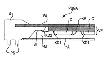
- the drawing shows a highly simplified schematic representation a section through part of a polymer stud Grid Arrays PSGA contacted with a wire bond technique VE wiring element.
- the basis of the array shown is a substrate S, which with "Polymer Studs” or polymer bumps PS and a depression M. is, the trough has a step labeled ST.
- the bottom of the trough M is through a heat sink WL formed. It can be seen that this heat sink WL is formed by a disc, the edge area in the Substrate material is embedded. The disc-shaped heat conducting body If necessary, WL could also join the outside world additional cooling fins can be provided.
- the production of the Substrate S including polymer bumps PS, trough M and Stage ST is carried out by injection molding, using as substrate materials high temperature resistant thermoplastics, e.g. Polyetherimide are suitable. Injection molding is done simultaneously also the one made of metal or ceramic, for example Thermally conductive body WL anchored in the substrate material at the edge.
- the wiring element VE is in the illustrated embodiment from a ceramic plate KP with its back is glued to the heat conducting body WL, and on the Front several chips C are applied.
- the connections of the chips C are also assigned via contact wires KD1 Connections one on the front of the ceramic plate KP formed wiring layer, not recognizable in the drawing connected.
- the connections of the wiring element VE are via contact wires KD2 with the internal connections of the array connected to the ST level of the trough M arranged, but not recognizable in the drawing are.
- the external connections formed on the polymer bumps PS and the conductor tracks that connect these external connections to the Connect internal connections at level ST are in the Drawing also not recognizable. Manufacturing details and design of the external connections, the internal connections and the ladder trains, go from the international Application No. PCT / EP95 / 03763, the disclosure content of which Is part of the present application.
Description
- ein spritzgegossenes, dreidimensionales Substrat aus einem elektrisch isolierenden Polymer,
- auf der Unterseite des Substrats flächig angeordnete und beim Spritzgießen mitgeformte Polymerhöcker,
- auf den Polymerhöckern durch eine lötbare Endoberfläche gebildete Außenanschlüsse,
- zumindest auf der Unterseite des Substrats ausgebildete Leiterzüge, die die Außenanschlüsse mit Innenanschlüssen verbinden, und
- mindestens einen auf dem Substrat angeordneten Chip, dessen Anschlüsse mit den Innenanschlüssen elektrisch leitend verbunden sind.
Claims (10)
- Polymer Stud Grid Array
miteinem spritzgegossenen, dreidimensionalens Substrat (S) aus einem elektrisch isolierenden Polymer,auf der Unterseite des Substrats (S) flächig angeordneten und beim Spritzgießen mitgeformte Polymerhöckern (PS),auf den Polymerhöckern (PS) durch eine lötbare Endoberfläche gebildeten Außenanschlüssen,zumindest auf der Unterseite des Substrats (S) ausgebildeten Leiterzügen, die die Außenanschlüsse mit Innenanschlüssen verbinden,mindestens einem beim Spritzgießen des Substrats (S) teilweise umspritzten Wärmeleitkörper (WL), und mitmindestens einem auf dem Wärmeleitkörper (WL) angeordnetenChip oder Verdrahtungselement (VE), dessen Anschlüsse mit den Innenanschlüssen elektrisch leitend verbunden sind. - Polymer Stud Grid Array nach Anspruch 1,
dadurch gekennzeichnet,
daß der Chip oder das Verdrahtungselement (VE) in einer Mulde (M) des Substrats (S) angeordnet ist, deren Boden durch den Wärmeleitkörper (WL) gebildet ist. - Polymer Stud Grid Array nach Anspruch 1 oder 2,
dadurch gekennzeichnet,
daß der Wärmeleitkörper (WL) durch eine randseitig in das Substrat eingebettete Scheibe gebildet ist. - Polymer Stud Grid Array nach Anspruch 1 bis 3,
dadurch gekennzeichnet,
daß der Wärmeleitkörper (WL) aus einem Material besteht, welches die Wärme besonders gut weiterleitet und das sich beim Erwärmen nur geringfügig ausdehnt. - Polymer Stud Grid Array nach einem der Ansprüche 1 bis 4, gekennzeichnet durch einen Wärmeleitkörper (WL) aus Metall.
- Polymer Stud Grid Array nach Anspruch 5,
dadurch gekennzeichnet,
daß der Wärmeleitkörper (WL) aus einer Chromlegierung, einer Nickellegierung oder einer Chromnickellegierung besteht. - Polymer Stud Grid Array nach einem der Ansprüche 1 bis 4,
gekennzeichnet durch einen Wärmeleitkörper (WL) aus Keramik. - Polymer Stud Grid Array nach Anspruch 7,
dadurch gekennzeichnet,
daß der Wärmeleitkörper (WL) aus Aluminiumoxid besteht. - Polymer Stud Grid Array nach einem der Ansprüche 1 bis 8,
dadurch gekennzeichnet,
daß der Chip oder das Verdrahtungselement (VE) auf den Wärmeleitkörper (WL) aufgeklebt ist. - Polymer Stud Grid Array nach einem der Ansprüche 2 bis 9,
dadurch gekennzeichnet,
daß die Mulde (M) mit einer Abdeckung (A) verschlossen ist.
Applications Claiming Priority (3)
| Application Number | Priority Date | Filing Date | Title |
|---|---|---|---|
| DE19538464 | 1995-10-16 | ||
| DE19538464 | 1995-10-16 | ||
| PCT/EP1996/004407 WO1997015078A1 (de) | 1995-10-16 | 1996-10-10 | Polymer stud grid array |
Publications (2)
| Publication Number | Publication Date |
|---|---|
| EP0856199A1 EP0856199A1 (de) | 1998-08-05 |
| EP0856199B1 true EP0856199B1 (de) | 2001-08-22 |
Family
ID=7774969
Family Applications (1)
| Application Number | Title | Priority Date | Filing Date |
|---|---|---|---|
| EP96934620A Expired - Lifetime EP0856199B1 (de) | 1995-10-16 | 1996-10-10 | Polymeres höcker-matrix-gehäuse |
Country Status (8)
| Country | Link |
|---|---|
| US (1) | US6122172A (de) |
| EP (1) | EP0856199B1 (de) |
| JP (1) | JP3037440B2 (de) |
| KR (1) | KR100430325B1 (de) |
| AT (1) | ATE204678T1 (de) |
| DE (1) | DE59607546D1 (de) |
| ES (1) | ES2163043T3 (de) |
| WO (1) | WO1997015078A1 (de) |
Families Citing this family (11)
| Publication number | Priority date | Publication date | Assignee | Title |
|---|---|---|---|---|
| US6705388B1 (en) * | 1997-11-10 | 2004-03-16 | Parker-Hannifin Corporation | Non-electrically conductive thermal dissipator for electronic components |
| DE10030289B4 (de) * | 1999-06-29 | 2012-10-04 | Marquardt Gmbh | Träger für Bauteile und Herstellungsverfahren |
| US6444489B1 (en) | 2000-12-15 | 2002-09-03 | Charles W. C. Lin | Semiconductor chip assembly with bumped molded substrate |
| US6486549B1 (en) | 2001-11-10 | 2002-11-26 | Bridge Semiconductor Corporation | Semiconductor module with encapsulant base |
| US6666693B2 (en) | 2001-11-20 | 2003-12-23 | Fci Americas Technology, Inc. | Surface-mounted right-angle electrical connector |
| US6638082B2 (en) | 2001-11-20 | 2003-10-28 | Fci Americas Technology, Inc. | Pin-grid-array electrical connector |
| US20050031840A1 (en) * | 2003-08-05 | 2005-02-10 | Xerox Corporation | RF connector |
| US7052763B2 (en) * | 2003-08-05 | 2006-05-30 | Xerox Corporation | Multi-element connector |
| DE102004032371A1 (de) * | 2004-06-30 | 2006-01-26 | Robert Bosch Gmbh | Elektronische Schaltungseinheit |
| US20090323295A1 (en) * | 2008-06-30 | 2009-12-31 | Houle Sabina J | Injection molded metal stiffener and integrated carrier for packaging applications |
| US10128593B1 (en) | 2017-09-28 | 2018-11-13 | International Business Machines Corporation | Connector having a body with a conductive layer common to top and bottom surfaces of the body as well as to wall surfaces of a plurality of holes in the body |
Citations (2)
| Publication number | Priority date | Publication date | Assignee | Title |
|---|---|---|---|---|
| EP0322434A1 (de) * | 1987-07-03 | 1989-07-05 | DODUCO GMBH + Co Dr. Eugen DÀ¼rrwächter | Flacher körper, insbesondere zur verwendung als wärmesenke für elektronische leistungsbauelemente |
| JPH03188654A (ja) * | 1989-12-18 | 1991-08-16 | Nippon Steel Corp | 樹脂モールド型半導体用放熱体 |
Family Cites Families (16)
| Publication number | Priority date | Publication date | Assignee | Title |
|---|---|---|---|---|
| US3271507A (en) * | 1965-11-02 | 1966-09-06 | Alloys Unltd Inc | Flat package for semiconductors |
| WO1989000346A1 (en) * | 1987-07-01 | 1989-01-12 | Western Digital Corporation | Plated plastic castellated interconnect for electrical components |
| DE3732249A1 (de) * | 1987-09-24 | 1989-04-13 | Siemens Ag | Verfahren zur herstellung von dreidimensionalen leiterplatten |
| US5438481A (en) * | 1987-11-17 | 1995-08-01 | Advanced Interconnections Corporation | Molded-in lead frames |
| US5152057A (en) * | 1987-11-17 | 1992-10-06 | Mold-Pac Corporation | Molded integrated circuit package |
| US5072283A (en) * | 1988-04-12 | 1991-12-10 | Bolger Justin C | Pre-formed chip carrier cavity package |
| US4868349A (en) * | 1988-05-09 | 1989-09-19 | National Semiconductor Corporation | Plastic molded pin-grid-array power package |
| US5081520A (en) * | 1989-05-16 | 1992-01-14 | Minolta Camera Kabushiki Kaisha | Chip mounting substrate having an integral molded projection and conductive pattern |
| EP1020914B1 (de) * | 1989-10-09 | 2004-04-28 | Mitsubishi Materials Corporation | Keramiksubstrat zur Herstellung elektrischer oder elektronischer Schaltungen |
| US5012386A (en) * | 1989-10-27 | 1991-04-30 | Motorola, Inc. | High performance overmolded electronic package |
| WO1992002040A1 (en) * | 1990-07-25 | 1992-02-06 | Dsm N.V. | Package for incorporating an integrated circuit and a process for the production of the package |
| JPH04322452A (ja) * | 1991-04-23 | 1992-11-12 | Mitsubishi Electric Corp | 半導体装置、半導体素子収納容器および半導体装置の製造方法 |
| JP2931741B2 (ja) * | 1993-09-24 | 1999-08-09 | 株式会社東芝 | 半導体装置 |
| EP0645953B1 (de) * | 1993-09-29 | 1997-08-06 | Siemens NV | Verfahren zur Herstellung einer zwei- oder mehrlagigen Verdrahtung und danach hergestellte zwei- oder mehrlagige Verdrahtung |
| ES2148564T3 (es) * | 1994-09-23 | 2000-10-16 | Siemens Nv | Bloque de matriz con proyecciones de polimero. |
| US5609889A (en) * | 1995-05-26 | 1997-03-11 | Hestia Technologies, Inc. | Apparatus for encapsulating electronic packages |
-
1996
- 1996-10-10 KR KR10-1998-0702732A patent/KR100430325B1/ko not_active IP Right Cessation
- 1996-10-10 AT AT96934620T patent/ATE204678T1/de not_active IP Right Cessation
- 1996-10-10 WO PCT/EP1996/004407 patent/WO1997015078A1/de active IP Right Grant
- 1996-10-10 ES ES96934620T patent/ES2163043T3/es not_active Expired - Lifetime
- 1996-10-10 US US09/051,778 patent/US6122172A/en not_active Expired - Fee Related
- 1996-10-10 DE DE59607546T patent/DE59607546D1/de not_active Expired - Fee Related
- 1996-10-10 EP EP96934620A patent/EP0856199B1/de not_active Expired - Lifetime
- 1996-10-10 JP JP09515493A patent/JP3037440B2/ja not_active Expired - Fee Related
Patent Citations (2)
| Publication number | Priority date | Publication date | Assignee | Title |
|---|---|---|---|---|
| EP0322434A1 (de) * | 1987-07-03 | 1989-07-05 | DODUCO GMBH + Co Dr. Eugen DÀ¼rrwächter | Flacher körper, insbesondere zur verwendung als wärmesenke für elektronische leistungsbauelemente |
| JPH03188654A (ja) * | 1989-12-18 | 1991-08-16 | Nippon Steel Corp | 樹脂モールド型半導体用放熱体 |
Also Published As
| Publication number | Publication date |
|---|---|
| WO1997015078A1 (de) | 1997-04-24 |
| ES2163043T3 (es) | 2002-01-16 |
| US6122172A (en) | 2000-09-19 |
| DE59607546D1 (de) | 2001-09-27 |
| KR19990064244A (ko) | 1999-07-26 |
| JPH11502064A (ja) | 1999-02-16 |
| KR100430325B1 (ko) | 2004-09-18 |
| JP3037440B2 (ja) | 2000-04-24 |
| ATE204678T1 (de) | 2001-09-15 |
| EP0856199A1 (de) | 1998-08-05 |
Similar Documents
| Publication | Publication Date | Title |
|---|---|---|
| EP0782765B1 (de) | Polymer stud grid array package | |
| EP0856198B1 (de) | Polymeres höcker-matrix-gehäuse für mikrowellen-schaltungsanordnungen | |
| DE4421077B4 (de) | Halbleitergehäuse und Verfahren zu dessen Herstellung | |
| CA1187674A (en) | Cast solder leads for leadless semiconductor circuits | |
| DE69935628T2 (de) | Hybridmodul | |
| DE102009002191B4 (de) | Leistungshalbleitermodul, Leistungshalbleitermodulanordnung und Verfahren zur Herstellung einer Leistungshalbleitermodulanordnung | |
| DE4017697C2 (de) | Elektronisches Bauelement, Verfahren zu dessen Herstellung und Verwendung | |
| DE10013255B4 (de) | Harzgekapselte elektronische Vorrichtung zur Verwendung in Brennkraftmaschinen | |
| DE69432968T2 (de) | Gehäuse für elektronische Bauelemente | |
| DE102009045063C5 (de) | Leistungshalbleitermodul mit angespritztem Kühlkörper, Leistungshalbleitermodulsystem und Verfahren zur Herstellung eines Leistungshalbleitermoduls | |
| DE10229692A1 (de) | Leiterplatte, Mehrchippackung und zugehöriges Herstellungsverfahren | |
| EP0856199B1 (de) | Polymeres höcker-matrix-gehäuse | |
| DE102012112769A1 (de) | Modul mit einer diskreten Vorrichtung, die auf einem DCB-Substrat montiert ist | |
| KR970073251A (ko) | 중계 기판, 그 제조 방법, 기판과 중계 기판과 부착 기판으로 이루어지는 구조체, 기판과 중계 기판의 접속체(A Connecting Board, a Method of Making a Connecting Board, an Assembly Consisting of a Base Plate, a Connecting Board and a Mounting Board, and a Subassembly of a Base Plate and a Connecting Board) | |
| WO2008009524A1 (de) | Elektronikanordnung | |
| EP1106040B1 (de) | Verfahren zur herstellung von verdrahtungen mit elektrisch leitenden querverbindungen zwischen ober- und unterseite eines substrats sowie verdrahtung mit derartigen querverbindungen | |
| DE10157362B4 (de) | Leistungsmodul und Verfahren zu seiner Herstellung | |
| EP1309998B1 (de) | Verfahren zur elektrischen verbindung eines halbleiterbauelements mit einer elektrischen baugruppe | |
| DE19830158C2 (de) | Zwischenträgersubstrat mit hoher Verdrahtungsdichte für elektronische Bauelemente | |
| DE102006024147B3 (de) | Elektronisches Modul mit Halbleiterbauteilgehäuse und einem Halbleiterchip und Verfahren zur Herstellung desselben | |
| WO1998000865A1 (de) | Modul für ein elektrisches gerät | |
| DE10310616B3 (de) | Modul mit Schaltungsträger und elektrooptischem Wandler sowie Verfahren zur Herstellung desselben | |
| WO2000072378A1 (de) | Substrat mit mindestens zwei metallisierten polymerhöckern für die lötverbindung mit einer verdrahtung | |
| DE10297766T5 (de) | Wärmeableitungsvorrichtung für Integrierte Schaltungen | |
| WO1999010926A1 (de) | Verfahren zur herstellung von elektrisch leitenden querverbindungen zwischen zwei verdrahtungslagen auf einem substrat |
Legal Events
| Date | Code | Title | Description |
|---|---|---|---|
| PUAI | Public reference made under article 153(3) epc to a published international application that has entered the european phase |
Free format text: ORIGINAL CODE: 0009012 |
|
| 17P | Request for examination filed |
Effective date: 19980406 |
|
| AK | Designated contracting states |
Kind code of ref document: A1 Designated state(s): AT BE CH DE ES FI FR GB IT LI NL |
|
| 17Q | First examination report despatched |
Effective date: 19990824 |
|
| GRAG | Despatch of communication of intention to grant |
Free format text: ORIGINAL CODE: EPIDOS AGRA |
|
| GRAG | Despatch of communication of intention to grant |
Free format text: ORIGINAL CODE: EPIDOS AGRA |
|
| GRAG | Despatch of communication of intention to grant |
Free format text: ORIGINAL CODE: EPIDOS AGRA |
|
| GRAH | Despatch of communication of intention to grant a patent |
Free format text: ORIGINAL CODE: EPIDOS IGRA |
|
| GRAH | Despatch of communication of intention to grant a patent |
Free format text: ORIGINAL CODE: EPIDOS IGRA |
|
| GRAA | (expected) grant |
Free format text: ORIGINAL CODE: 0009210 |
|
| AK | Designated contracting states |
Kind code of ref document: B1 Designated state(s): AT BE CH DE ES FI FR GB IT LI NL |
|
| REF | Corresponds to: |
Ref document number: 204678 Country of ref document: AT Date of ref document: 20010915 Kind code of ref document: T |
|
| REG | Reference to a national code |
Ref country code: CH Ref legal event code: EP |
|
| REF | Corresponds to: |
Ref document number: 59607546 Country of ref document: DE Date of ref document: 20010927 |
|
| REG | Reference to a national code |
Ref country code: CH Ref legal event code: NV Representative=s name: SIEMENS SCHWEIZ AG |
|
| GBT | Gb: translation of ep patent filed (gb section 77(6)(a)/1977) |
Effective date: 20011117 |
|
| REG | Reference to a national code |
Ref country code: GB Ref legal event code: IF02 |
|
| REG | Reference to a national code |
Ref country code: ES Ref legal event code: FG2A Ref document number: 2163043 Country of ref document: ES Kind code of ref document: T3 |
|
| ET | Fr: translation filed | ||
| PLBE | No opposition filed within time limit |
Free format text: ORIGINAL CODE: 0009261 |
|
| STAA | Information on the status of an ep patent application or granted ep patent |
Free format text: STATUS: NO OPPOSITION FILED WITHIN TIME LIMIT |
|
| 26N | No opposition filed | ||
| PGFP | Annual fee paid to national office [announced via postgrant information from national office to epo] |
Ref country code: FI Payment date: 20020910 Year of fee payment: 7 |
|
| PGFP | Annual fee paid to national office [announced via postgrant information from national office to epo] |
Ref country code: AT Payment date: 20021004 Year of fee payment: 7 |
|
| PGFP | Annual fee paid to national office [announced via postgrant information from national office to epo] |
Ref country code: ES Payment date: 20021018 Year of fee payment: 7 |
|
| PGFP | Annual fee paid to national office [announced via postgrant information from national office to epo] |
Ref country code: NL Payment date: 20021021 Year of fee payment: 7 |
|
| PGFP | Annual fee paid to national office [announced via postgrant information from national office to epo] |
Ref country code: CH Payment date: 20030115 Year of fee payment: 7 |
|
| PG25 | Lapsed in a contracting state [announced via postgrant information from national office to epo] |
Ref country code: FI Free format text: LAPSE BECAUSE OF NON-PAYMENT OF DUE FEES Effective date: 20031010 Ref country code: AT Free format text: LAPSE BECAUSE OF NON-PAYMENT OF DUE FEES Effective date: 20031010 |
|
| PG25 | Lapsed in a contracting state [announced via postgrant information from national office to epo] |
Ref country code: ES Free format text: LAPSE BECAUSE OF NON-PAYMENT OF DUE FEES Effective date: 20031011 |
|
| PG25 | Lapsed in a contracting state [announced via postgrant information from national office to epo] |
Ref country code: LI Free format text: LAPSE BECAUSE OF NON-PAYMENT OF DUE FEES Effective date: 20031031 Ref country code: CH Free format text: LAPSE BECAUSE OF NON-PAYMENT OF DUE FEES Effective date: 20031031 |
|
| PG25 | Lapsed in a contracting state [announced via postgrant information from national office to epo] |
Ref country code: NL Free format text: LAPSE BECAUSE OF NON-PAYMENT OF DUE FEES Effective date: 20040501 |
|
| REG | Reference to a national code |
Ref country code: CH Ref legal event code: PL |
|
| NLV4 | Nl: lapsed or anulled due to non-payment of the annual fee |
Effective date: 20040501 |
|
| PGFP | Annual fee paid to national office [announced via postgrant information from national office to epo] |
Ref country code: GB Payment date: 20041012 Year of fee payment: 9 |
|
| PGFP | Annual fee paid to national office [announced via postgrant information from national office to epo] |
Ref country code: BE Payment date: 20041020 Year of fee payment: 9 |
|
| PGFP | Annual fee paid to national office [announced via postgrant information from national office to epo] |
Ref country code: FR Payment date: 20041029 Year of fee payment: 9 |
|
| PGFP | Annual fee paid to national office [announced via postgrant information from national office to epo] |
Ref country code: DE Payment date: 20041220 Year of fee payment: 9 |
|
| REG | Reference to a national code |
Ref country code: ES Ref legal event code: FD2A Effective date: 20031011 |
|
| PG25 | Lapsed in a contracting state [announced via postgrant information from national office to epo] |
Ref country code: IT Free format text: LAPSE BECAUSE OF NON-PAYMENT OF DUE FEES;WARNING: LAPSES OF ITALIAN PATENTS WITH EFFECTIVE DATE BEFORE 2007 MAY HAVE OCCURRED AT ANY TIME BEFORE 2007. THE CORRECT EFFECTIVE DATE MAY BE DIFFERENT FROM THE ONE RECORDED. Effective date: 20051010 Ref country code: GB Free format text: LAPSE BECAUSE OF NON-PAYMENT OF DUE FEES Effective date: 20051010 |
|
| PG25 | Lapsed in a contracting state [announced via postgrant information from national office to epo] |
Ref country code: BE Free format text: LAPSE BECAUSE OF NON-PAYMENT OF DUE FEES Effective date: 20051031 |
|
| PG25 | Lapsed in a contracting state [announced via postgrant information from national office to epo] |
Ref country code: DE Free format text: LAPSE BECAUSE OF NON-PAYMENT OF DUE FEES Effective date: 20060503 |
|
| GBPC | Gb: european patent ceased through non-payment of renewal fee |
Effective date: 20051010 |
|
| PG25 | Lapsed in a contracting state [announced via postgrant information from national office to epo] |
Ref country code: FR Free format text: LAPSE BECAUSE OF NON-PAYMENT OF DUE FEES Effective date: 20060630 |
|
| REG | Reference to a national code |
Ref country code: FR Ref legal event code: ST Effective date: 20060630 |
|
| BERE | Be: lapsed |
Owner name: *INTERUNIVERSITAIRE MICRO-ELEKTRONICA CENTRUM V.Z. Effective date: 20051031 Owner name: *SIEMENS N.V. Effective date: 20051031 |