EP0855798B1 - Schaltungsanordnung zum Erzeugen eines Ausgangssignals - Google Patents
Schaltungsanordnung zum Erzeugen eines Ausgangssignals Download PDFInfo
- Publication number
- EP0855798B1 EP0855798B1 EP98200089A EP98200089A EP0855798B1 EP 0855798 B1 EP0855798 B1 EP 0855798B1 EP 98200089 A EP98200089 A EP 98200089A EP 98200089 A EP98200089 A EP 98200089A EP 0855798 B1 EP0855798 B1 EP 0855798B1
- Authority
- EP
- European Patent Office
- Prior art keywords
- output
- input
- signal
- threshold value
- threshold
- Prior art date
- Legal status (The legal status is an assumption and is not a legal conclusion. Google has not performed a legal analysis and makes no representation as to the accuracy of the status listed.)
- Expired - Lifetime
Links
- 230000003111 delayed effect Effects 0.000 claims description 5
- 230000007704 transition Effects 0.000 claims description 2
- 230000008878 coupling Effects 0.000 claims 1
- 238000010168 coupling process Methods 0.000 claims 1
- 238000005859 coupling reaction Methods 0.000 claims 1
- 230000006870 function Effects 0.000 description 6
- 230000000630 rising effect Effects 0.000 description 6
- 238000010586 diagram Methods 0.000 description 4
- 238000011156 evaluation Methods 0.000 description 3
- 230000005540 biological transmission Effects 0.000 description 2
- 230000035945 sensitivity Effects 0.000 description 2
- 238000010276 construction Methods 0.000 description 1
- 230000007423 decrease Effects 0.000 description 1
- 230000002950 deficient Effects 0.000 description 1
- 230000001934 delay Effects 0.000 description 1
- 230000001419 dependent effect Effects 0.000 description 1
- 230000000694 effects Effects 0.000 description 1
- 230000036039 immunity Effects 0.000 description 1
- 230000002452 interceptive effect Effects 0.000 description 1
Images


Classifications
-
- H—ELECTRICITY
- H03—ELECTRONIC CIRCUITRY
- H03K—PULSE TECHNIQUE
- H03K5/00—Manipulating of pulses not covered by one of the other main groups of this subclass
- H03K5/01—Shaping pulses
- H03K5/08—Shaping pulses by limiting; by thresholding; by slicing, i.e. combined limiting and thresholding
- H03K5/082—Shaping pulses by limiting; by thresholding; by slicing, i.e. combined limiting and thresholding with an adaptive threshold
- H03K5/086—Shaping pulses by limiting; by thresholding; by slicing, i.e. combined limiting and thresholding with an adaptive threshold generated by feedback
- H03K5/088—Shaping pulses by limiting; by thresholding; by slicing, i.e. combined limiting and thresholding with an adaptive threshold generated by feedback modified by switching, e.g. by a periodic signal or by a signal in synchronism with the transitions of the output signal
-
- H—ELECTRICITY
- H03—ELECTRONIC CIRCUITRY
- H03K—PULSE TECHNIQUE
- H03K5/00—Manipulating of pulses not covered by one of the other main groups of this subclass
- H03K5/01—Shaping pulses
- H03K5/08—Shaping pulses by limiting; by thresholding; by slicing, i.e. combined limiting and thresholding
- H03K5/082—Shaping pulses by limiting; by thresholding; by slicing, i.e. combined limiting and thresholding with an adaptive threshold
- H03K5/084—Shaping pulses by limiting; by thresholding; by slicing, i.e. combined limiting and thresholding with an adaptive threshold modified by switching, e.g. by a periodic signal or by a signal in synchronism with the transitions of the output signal
Definitions
- the invention relates to a circuit arrangement for generating a Output signal having a plurality of predetermined values, which is substantially change seamlessly, from a much slower changing Input signal.
- each device triggering the transmission of a message can (multi-master operation), to avoid conflicts on the bus each Signal a predetermined time after the beginning of the leading edge of the signal sampled and evaluated only the signal state during the scan.
- the signal edges can be relatively flat, so that the Duration of each signal must not fall below a certain value. This will the maximum frequency of the signals and thus transmission capacity on the bus limited.
- the Input signal exceeds both the higher threshold and the lower threshold.
- the object of the invention is a circuit arrangement of the type mentioned specify the fastest possible evaluation of an input signal change allows and also with input signals with a lower stroke and a Offset in the order of magnitude of this lower signal swing still largely works reliably.
- the threshold at the output signal changes the value at the rising edge of the Input signal is low and high at the falling edge of the input signal. Switching between these two thresholds will depend on the Input signal carried out, and in other thresholds, the different from the first mentioned thresholds.
- the Switching to the higher threshold occurs when the rising edge of the input signal has exceeded at least this higher threshold, and the switch back to the lower threshold occurs when at the falling edge of the input signal at least this lower threshold is fallen short of.
- the change of the output signal can be done earlier than in known circuits, namely shortly after the beginning of the rising or the falling edge. An inevitable consequence of this measure, however, is that the signal-to-noise ratio is reduced, at least for certain interference signals. this will compensated in that, in a known manner, the input signal a certain Time interval is scanned after the first change of the output signal.
- the principle of the invention can also be applied if the output signal is not binary, but can take more than two values. That's what then correspondingly more thresholds required. Switching the Switching threshold from the lower or first threshold to the upper or second threshold Threshold can occur when the input signal has a third threshold exceeded, which may be greater than or equal to the second threshold, and accordingly, the switching of the switching threshold to the first Threshold occur when the input signal has a fourth threshold is less than or equal to the first threshold. at Equality of thresholds can be greater insensitivity to Strörsignale be achieved when switching after reaching the corresponding threshold is delayed.
- a concrete embodiment of the circuit arrangement according to the invention can be that used to generate the output signal, a comparator which compares the input signal to a threshold and equality the value of the output signal changes, the threshold by a additional switching device is switched depending on the input signal. If the comparator at the respective threshold, a switching hysteresis has the sensitivity to noise in the input signal reduced.
- Two comparators are used, one of which is the input signal with the first threshold and the other compares to the second threshold.
- the Outputs of the two comparators lead to a switch, which depends on third or fourth threshold value is switched, and thus the output signal decreases from the output of one or the other comparator. This works in exactly the same as the switching of the threshold value in use only one comparator for the first and second thresholds.
- Also in this Traps may be the two comparators or at least one of them Have switching hysteresis to reduce the sensitivity to noise in Reduce input signal.
- Switching the threshold value when using a comparator or the Output signal when using two comparators is done with the help of a Switching device controlled by the input signal.
- This one can Threshold switch with hysteresis included, where the switching points equal to the third and fourth threshold, respectively. But it can also be for each of these Both thresholds can be used a separate comparator, and both Comparators control a memory stage whose output is the switchover causes. In the latter embodiment and the use of two Comparators for generating the output signal may also be the signals to The outputs of these comparators are used directly to control the memory level become. This results in a particularly simple structure.
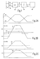
- Fig. 1 In the block diagram of Fig. 1 are on two lines 61 and 62 signals in Push differential, as shown in Fig. 2a with the voltage curves for the Signal voltages Ua and Ub is shown. These two signal voltages will be fed to a stage 64, the difference Ua - Ub of the two Signal voltages forms, which are output as signal voltage Uc on the line 65 becomes.
- the line 65 leads to a block 66, the inventive Contains circuitry and outputs with steep edges on the Line 67 generated. These are fed to a processing arrangement 68 which will not be explained in detail here, since it does not belong to the invention.
- the circuit arrangement according to the invention in block 66 is now constructed so that the signal on the line 67 already changes its value when the Signal voltage Uc exceeds a lower threshold V1. If the Signal voltage Uc an upper threshold V2 or even higher Threshold exceeds the switching threshold of the circuit in Block 66 is switched to the threshold V2, and thereby the signal changes on the line 67 its value at the falling edge of the signal voltage Uc, when the second threshold V2 is exceeded. In both cases, so early after the beginning of a change of the signal voltage Uc an output signal generated, so that a faster or earlier evaluation of the signal changes the lines 61 and 62 is possible.
- Fig. 2c the waveform of the signal voltage Uc is shown for the cases that the Line 61 or the line 62 is defective, for example by the relevant Line short to ground or to supply voltage has.
- Signal curve U'c is assumed that the voltage Ua is constantly high Potential or the voltage Ub is constantly at reference potential.
- the signal voltage U "c assumed that the voltage Ub constantly is at a high potential or the voltage Ua has constant reference potential. It is to recognize that the voltage U'c never crosses the lower threshold V1, so that constantly the upper threshold V2 remains effective. Run through accordingly the signal voltage U "c never exceeds the upper threshold V2, so that this constantly the lower threshold V1 remains effective. In both cases, so with the circuit according to the invention generates an output signal.
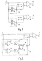
- FIG. 3 shows an embodiment of the circuit arrangement shown in FIG. 1 is indicated by the block 66.
- This circuit is used in this Example for generating three different values of the output signal, the two separate outputs 4a and 4b for each binary signal is delivered.
- One Signal input 2 for an input signal I is at a first input of two Comparators 6a and 6b are connected, which have a second input, with a switch 8a and 8b is connected.
- the output signal of the comparator 6a or 6b which is output at the output 4a or 4b, changes the binary State when the signal voltage at the first input of the relevant comparator the voltage at the second input exceeds or falls below.
- the second Input of the comparator 6a or 6b is dependent on the position of Switch 8a and 8b, a first threshold V1 or V'1 or a second Threshold V2 or V'2 supplied.
- the position of the switches 8a and 8b is by a switching device 10a or 10 b controlled, which has an input, which is also connected to the signal input 2 connected is.
- the switching device 10a which controls the changeover switch 8a, contains a Schmitt trigger 12a whose output signal from a first value to a second value changes when an upper threshold V3 is exceeded, and whose output signal assumes the first value again, if thereafter a lower one Switching threshold V4 is exceeded.
- a Schmitt trigger 12b whose output signal is the value changes if an upper switching threshold V'3 exceeded or a lower Switching threshold V'4 is exceeded.
- Fig. 4a is an input signal with a linearly rising and falling edge shown. Go through these flanks different thresholds V1 to V4 and V'1 to V'4, respectively, in this example it is assumed that the threshold value V3 is equal to the threshold value V'4.
- the switches 8a and 8b are in the position shown in FIG Position.
- the comparators 6a and 6b give a low signal at the outputs 4a and 4b, if the input signal I below the threshold V1 or V'1 lies. If the input signal is the threshold V1 at time t1 exceeds the output O1 at the output 4a to a high value, as shown in Fig. 4b. If the input signal I is the threshold V2 goes through, a signal changes in the circuit of Fig. 3k. First if the threshold V3 is exceeded at the time t2, the Switching device 10a the switch 8a to the threshold value V2, as shown in FIG. 4c is shown. However, since threshold V2 is below threshold V3 is, the output signal O1 does not change its value.
- the output signal O2 of the comparator 6b goes to a high Value, as shown in Fig. 4d.
- the threshold value V'2 is exceeded there is again no signal change, while when exceeding the Threshold V'3 at time t4, the switching device 10b the switch 8b to the threshold V'2 switches.
- the output O2 of the comparator 6b does not change its value.
- the threshold value is reached at time t5 Go through V'2, and thus the output signal O2 goes back to a low Value. If, at the time t6, the threshold value V'4 is exceeded, switches the switching device 10b the switch 8b back to the lower threshold V'1 back. Because this threshold but above the input signal at Time t6 is located, the output signal O2 does not change.
- the threshold V2 is exceeded, and it works the output signal O1 back to a low value. Finally, the Time t8 the threshold V4 falls below, and thus switches the Switching device 10a the switch 8a back to the threshold V1. In order to the initial state is restored.
- the output signals O1 and O2 both in the rising edge as well as at the falling edge of the input signal I to Change the value at a relatively early stage.
- the threshold V'4 is here only for example equal to the threshold V3, in fact, can however, the thresholds V1 to V4 are arbitrarily opposite to the thresholds V'1 to be shifted to V'4 because they are independent of each other. It's easy too to see that the circuit of FIG. 3 by additional comparators and Switching devices can be extended if more than three different Output signals are to be generated. In the following description of the others Embodiments is assumed for the sake of simplicity that a Output signal with only two different values to be generated.
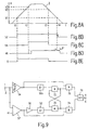
- FIG. 5 shows a circuit arrangement which likewise has a comparator 6 and a changeover switch 8, but in which the switching device 20 for the Switch 8 is constructed differently than in the circuit of Fig. 3.
- the Switching device 20 includes two comparators 22 and 24, each with a first Input, which is connected to the signal input 2 for the input signal I, and with a second input connected to the thresholds V3 and V4, respectively.
- the comparator 22 generates a high signal when the input signal I the Threshold V3 exceeds while comparator 24 only outputs a high signal generated when the input signal I is below the threshold V4, as by the circle at the output of the comparator 24 is indicated.
- the thresholds V1 to V4 are assumed as shown in FIG.
- the output of the comparator 22 is connected via a delay element 32 with a Input S of a flip-flop 26, while the output of the comparator 24th is connected to an input R of this flip-flop via a delay element 34.
- An output Q of the flip-flop 26 controls the switch 8.
- the input S is a high signal, and the output Q goes high and switches the switch 8 to the threshold V2, whereby the output signal 0 does not change.
- the signal at the input S the flip-flop 26 low again, but its state is maintained until the Signal falls below the threshold V4.
- the comparator 24 generates again a high signal, and the flip-flop 26 switches, causing the output Q to turn on low signal leads and the switch 8 back to the threshold V1 switches back.
- the output signal was 0 gone back to a low value.
- the switching device 20 in exactly behaves the same way as the switching device 10a of FIG. 3, when the Delays 32 and 34 are not taken into account. These cause that the flip-flop 26 is switched delayed, then the input voltage already higher than the threshold value V3 or a lower value than the threshold V4. This makes it possible for the Threshold voltage V3 only slightly greater than the threshold voltage V2 or even to choose the same. Accordingly, by the delay element 34, the Threshold voltage V4 only slightly lower than or equal to the Threshold voltage V1 can be selected. When both delay elements 32 and 34 They can also be used by a single dashed line Delay member 36 are replaced at the output of the flip-flop 26.
- Fig. 6 is not the Switched threshold voltage, but there are two comparators 42 and 44th provided, both of which are connected to the signal input 2 and of which the Comparator 42, the input signal with the threshold voltage V1 and the Comparator 44 compares the input signal with the threshold voltage V2.
- a changeover switch 48 which controls the signal output depending on the switch position with the output of the comparator 42 or the Comparator 44 connects.
- the switch 48 is controlled by a switching device 30th driven, in principle, in the same manner as the switching device 20 after Fig. 5 is constructed, only the delay elements are for clarity omitted.
- the sequence of Thresholds may be as indicated in the diagram of FIG. 4.
- First is the input signal I lower than the threshold value V4, so that the flip-flop 26th is brought into the reset state and the signal at the output Q low is and brings the switch in the drawn lower position. If that Input signal I exceeds the threshold V1, the signal is at the output of the comparator 42 and thus the output signal O at the signal output 4 high. If the input signal I thereafter exceeds the threshold value V2, so too the signal at the output of the comparator 44 is high, but this output is initially still open.
- circuit of FIG. 6 is the same Output signal generated as the circuit of FIG. 5.
- the difference in construction is that now two comparators 42 and 44 in addition to the Switching device 30 are used and that the switch with the outputs this comparator is connected.
- a significant Derive simplified circuit which is shown in Fig. 7.
- This contains one Comparator 52, of which one input to the signal input 2 and another Input is connected to the threshold V1. Further, a Schmitt trigger 54 present, which is also connected to the signal input 2 and the one Hysteresis between the thresholds V2 and V3 has. The output of the Comparator 52 and the Schmitt trigger 54 is connected to inputs of a changeover switch 48 connected, depending on the switch position, the output of one of these connects both elements with the signal output 4.
- the output of the comparator 52 is also via a delay element 50, here also by the circle has at the output indicated inverting function, with the input R of a Flip-flops 46 connected, and the output of the Schmitt trigger 54 is also with coupled to the input S of the flip-flop 46, wherein in this signal path also a Time delay element 50a may lie.
- the output Q of the flip-flop 46 controls the Switch 48.
- Fig. 8a is again the course of the input signal I and the location of thresholds V1, V2 and V3 are shown.
- the one with the before Threshold V4 used with the circuits described falls with the Threshold V1 together and is not specified separately.
- the input R of the flip-flop 46 receives a high signal and the flip-flop 46 in brings the reset position.
- the output Q has a low signal, so that the Switch 48 is in the drawn lower position.
- the signal at the output of the comparator 52 changes its value and becomes high, and thus also the output signal O at the signal output 4 becomes high, as shown in FIG. 8b and 8e is shown.
- the Schmitt carrier 54 outputs a high output Signal only when the input signal I is the threshold V3 at time t2 has exceeded, as shown in Fig. 8c.
- the flip-flop 46th switched immediately, if the delay element 50 does not exist, or delayed accordingly when the delay element 50a is present, as in Fig. 8d is shown.
- the output signal O at the signal output 4 changes its value is not, but remains high.
- the delay element 50 prevents the effect of small disturbances in the input signal I, because if at time t4, if the Threshold V1 is being traversed, small spurious signals on the Input signal I are present, the threshold value V1 a few times is exceeded and undershot, and corresponding signals then occur at the output of the comparator 52, as indicated in Fig. 8b. If that Delay element 50 would not exist at the first edge of the Signal at the output of the comparator 52, the flip-flop 46 tip over and the Changeover switch 48 to this output, so that the signal changes on Output of the comparator 52 would also appear at the signal output 4. By the delay element 50, the flip-flop 46 but only switched after These short signal changes at the output of the comparator 52 have decayed.
- the delay element 50 can be omitted, if comparator 52 is also used as a Schmitt carrier with a hysteresis between the threshold values V1 and V4 according to the sequence shown in FIG Thresholds is replaced.
- the Schmitt carrier 54 by be replaced by a simple comparator whose second input the Threshold V2 is obtained when the dashed line delay element 50a is available.
- the delay elements 50 and 50a may also be provided when the comparator 52 is executed as a Schmitt trigger to the Noise immunity of the circuit arrangement at both edges of the input signal in addition to increase.
- a circuit arrangement is shown, that of the circuit arrangement According to Fig. 7, when the switch 48 and the flip-flop 46 by individual Gates are realized.
- the output of the comparator 52 is connected to an input an AND gate 74 and an inverter 56 and a delay element 50 connected to an input of a NAND gate 70.
- the output of the Schmitt trigger 54 is connected to an input of an AND gate 76 and via a Delay member 50a is connected to an input of a NAND gate 72.
- the Outputs of NAND gates 70 and 72 are connected to another input of each other gate and with another input of the AND gate 74 and 76th connected.
- the outputs of the AND gates 74 and 76 lead to inputs of a OR gate 78 whose output is connected to the signal output 4.
- the NAND gates 70 and 72 form the flip-flop, while gates 74, 76 and 78 form the flip-flop Implement changeover switch.
- the function of the circuit of FIG. 9 is the same as FIG that of Fig. 7, as can
Landscapes
- Physics & Mathematics (AREA)
- Nonlinear Science (AREA)
- Manipulation Of Pulses (AREA)
Applications Claiming Priority (2)
| Application Number | Priority Date | Filing Date | Title |
|---|---|---|---|
| DE19702303 | 1997-01-23 | ||
| DE19702303A DE19702303A1 (de) | 1997-01-23 | 1997-01-23 | Schaltungsanordnung zum Erzeugen eines Ausgangssignals |
Publications (2)
| Publication Number | Publication Date |
|---|---|
| EP0855798A1 EP0855798A1 (de) | 1998-07-29 |
| EP0855798B1 true EP0855798B1 (de) | 2005-09-07 |
Family
ID=7818144
Family Applications (1)
| Application Number | Title | Priority Date | Filing Date |
|---|---|---|---|
| EP98200089A Expired - Lifetime EP0855798B1 (de) | 1997-01-23 | 1998-01-14 | Schaltungsanordnung zum Erzeugen eines Ausgangssignals |
Country Status (4)
| Country | Link |
|---|---|
| US (1) | US6111443A (enExample) |
| EP (1) | EP0855798B1 (enExample) |
| JP (1) | JP4159129B2 (enExample) |
| DE (2) | DE19702303A1 (enExample) |
Families Citing this family (8)
| Publication number | Priority date | Publication date | Assignee | Title |
|---|---|---|---|---|
| US6845348B1 (en) * | 2000-04-03 | 2005-01-18 | Lsi Logic Corporation | Driver waveform modeling with multiple effective capacitances |
| US7130340B1 (en) * | 2000-10-27 | 2006-10-31 | Sun Microsystems, Inc. | Noise margin self-diagnostic receiver logic |
| WO2002099619A1 (fr) * | 2001-05-30 | 2002-12-12 | Thine Electronics, Inc. | Circuit integre a semi-conducteur |
| US6828828B2 (en) * | 2001-08-03 | 2004-12-07 | Hewlett-Packard Development Company, L.P. | Dynamic control of switching reference voltage |
| DE10156026B4 (de) * | 2001-11-15 | 2007-02-22 | Advanced Micro Devices, Inc., Sunnyvale | Komparatorschaltung sowie Verfahren zum Bestimmen eines Zeitintervalls |
| US20090212845A1 (en) * | 2008-02-26 | 2009-08-27 | Honeywell International Inc. | High Voltage Control Switch |
| US8436659B1 (en) * | 2008-06-24 | 2013-05-07 | Marvell International Ltd. | Circuits and methods for reducing electrical stress on a transistor |
| DE102012015945A1 (de) * | 2012-08-09 | 2014-05-15 | Infineon Technologies Ag | Komparatorschaltung mit einer versteckten Hysterese |
Family Cites Families (11)
| Publication number | Priority date | Publication date | Assignee | Title |
|---|---|---|---|---|
| FR2511566A1 (fr) * | 1981-08-12 | 1983-02-18 | Thomson Csf | Recepteur optique a seuils pour systeme de transmission numerique a debit variable |
| GB2120030B (en) * | 1982-03-04 | 1986-11-12 | Sansui Electric Co | Digital signal demodulator circuit |
| JPS58155481A (ja) * | 1982-03-10 | 1983-09-16 | Ricoh Co Ltd | 画像2値化処理方式 |
| JPS60176324A (ja) * | 1984-02-22 | 1985-09-10 | Pioneer Electronic Corp | 波形整形回路 |
| DE3442613A1 (de) * | 1984-11-22 | 1986-05-22 | Siemens AG, 1000 Berlin und 8000 München | Synchronisierstufe zur gewinnung eines synchronisiersignals mit geringem jitter aus einer biternaeren datenfolge |
| JPH01265718A (ja) * | 1988-04-18 | 1989-10-23 | Toshiba Corp | シュミットトリガ回路 |
| NL8902225A (nl) * | 1989-09-05 | 1991-04-02 | Philips Nv | Schakeling voor het detekteren van impulsen, en videorecorder voorzien van de schakeling. |
| US5191462A (en) * | 1990-05-11 | 1993-03-02 | At&T Bell Laboratories | Fiber optic transmission distortion compensation |
| DE4221113C1 (de) * | 1992-06-26 | 1993-12-09 | Sick Optik Elektronik Erwin | Komparatorschaltung zur Auslösung eines Schaltvorganges beim Durchgang eines veränderlichen Meßsignals durch eine Schaltschwelle |
| US5373400A (en) * | 1993-12-01 | 1994-12-13 | Analog Devices, Inc. | Dynamic threshold updating circuit for a maximum likelihood detector using both positive and negative comparators |
| US5673282A (en) * | 1995-07-28 | 1997-09-30 | Lucent Technologies Inc. | Method and apparatus for monitoring performance of a laser transmitter |
-
1997
- 1997-01-23 DE DE19702303A patent/DE19702303A1/de not_active Withdrawn
-
1998
- 1998-01-14 EP EP98200089A patent/EP0855798B1/de not_active Expired - Lifetime
- 1998-01-14 DE DE59813036T patent/DE59813036D1/de not_active Expired - Lifetime
- 1998-01-21 JP JP00940798A patent/JP4159129B2/ja not_active Expired - Fee Related
- 1998-01-22 US US09/010,895 patent/US6111443A/en not_active Expired - Lifetime
Also Published As
| Publication number | Publication date |
|---|---|
| JPH10233662A (ja) | 1998-09-02 |
| DE19702303A1 (de) | 1998-07-30 |
| EP0855798A1 (de) | 1998-07-29 |
| JP4159129B2 (ja) | 2008-10-01 |
| US6111443A (en) | 2000-08-29 |
| DE59813036D1 (de) | 2005-10-13 |
Similar Documents
| Publication | Publication Date | Title |
|---|---|---|
| DE3708499C2 (enExample) | ||
| DE69404255T2 (de) | Quadraturoszillator | |
| DE69807592T2 (de) | Chopper-Komparator für Spannungen | |
| DE69720128T2 (de) | Schneller, verbrauchsarmer Chopper Komparator mit störungsfreier Funktion bei Variation des logischen Schwellwertes der Inverter | |
| DE2819524A1 (de) | Taktgesteuerte spannungsvergleichsschaltung | |
| DE2439937C3 (de) | Schaltungsanordnung zur Erzeugung eines gegenüber einem Eingangsimpuls verzögerten Ausgangsimpulses | |
| EP0855798B1 (de) | Schaltungsanordnung zum Erzeugen eines Ausgangssignals | |
| DE3633310A1 (de) | Anordnung zur formung von taktsignalen | |
| DE3032568C2 (de) | Generator für Taktsignale mit durch Befehlssignale steuerbarer Periodenlänge | |
| EP0977406B1 (de) | Schaltungsanordnung zum galvanisch getrennten Übertragen von Digitalsignalen | |
| EP0013686B1 (de) | Verriegelungsschaltung | |
| DE19905053C2 (de) | Komparatorschaltung | |
| DE2422123A1 (de) | Schaltverzoegerungsfreie bistabile schaltung | |
| DE69920780T2 (de) | Schaltung zum Steilermachen von Pulsflanken | |
| DE10223514B4 (de) | Komparatorschaltung | |
| DE69533604T2 (de) | Verriegelungsschaltung | |
| DE3604716C2 (enExample) | ||
| DE102005015429B3 (de) | Takterzeugung für einen zeitversetzt arbeitenden Analog-Digital-Wandler | |
| DE4318378A1 (de) | Schaltungsanordnung zur Unterdrückung von dynamischen Störungen in digitalen Schaltungen, insbesondere in integrierten Schaltkreisen | |
| DE19906860C2 (de) | Tristate-Differenz-Ausgangsstufe | |
| DE69303086T2 (de) | Phasen- und Frequenzkomparator | |
| EP0318080A2 (de) | Schaltungsanordnung für eine Doppel-Busleitung | |
| EP1112618B1 (de) | Digitale schaltung | |
| DE2945984C2 (de) | Schaltungsanordnung zur Signalisierung des Ausfalls periodischer Impulssignale | |
| DE2932745A1 (de) | Digitaler frequenz- und phasenvergleicher |
Legal Events
| Date | Code | Title | Description |
|---|---|---|---|
| PUAI | Public reference made under article 153(3) epc to a published international application that has entered the european phase |
Free format text: ORIGINAL CODE: 0009012 |
|
| AK | Designated contracting states |
Kind code of ref document: A1 Designated state(s): DE FR GB |
|
| RAP3 | Party data changed (applicant data changed or rights of an application transferred) |
Owner name: KONINKLIJKE PHILIPS ELECTRONICS N.V. Owner name: PHILIPS PATENTVERWALTUNG GMBH |
|
| 17P | Request for examination filed |
Effective date: 19990129 |
|
| AKX | Designation fees paid |
Free format text: DE FR GB |
|
| RBV | Designated contracting states (corrected) |
Designated state(s): DE FR GB |
|
| RAP3 | Party data changed (applicant data changed or rights of an application transferred) |
Owner name: KONINKLIJKE PHILIPS ELECTRONICS N.V. Owner name: PHILIPS CORPORATE INTELLECTUAL PROPERTY GMBH |
|
| RAP1 | Party data changed (applicant data changed or rights of an application transferred) |
Owner name: KONINKLIJKE PHILIPS ELECTRONICS N.V. Owner name: PHILIPS CORPORATE INTELLECTUAL PROPERTY GMBH |
|
| RAP1 | Party data changed (applicant data changed or rights of an application transferred) |
Owner name: KONINKLIJKE PHILIPS ELECTRONICS N.V. Owner name: PHILIPS INTELLECTUAL PROPERTY & STANDARDS GMBH |
|
| GRAP | Despatch of communication of intention to grant a patent |
Free format text: ORIGINAL CODE: EPIDOSNIGR1 |
|
| GRAS | Grant fee paid |
Free format text: ORIGINAL CODE: EPIDOSNIGR3 |
|
| GRAA | (expected) grant |
Free format text: ORIGINAL CODE: 0009210 |
|
| AK | Designated contracting states |
Kind code of ref document: B1 Designated state(s): DE FR GB |
|
| REG | Reference to a national code |
Ref country code: GB Ref legal event code: FG4D Free format text: NOT ENGLISH |
|
| REF | Corresponds to: |
Ref document number: 59813036 Country of ref document: DE Date of ref document: 20051013 Kind code of ref document: P |
|
| GBT | Gb: translation of ep patent filed (gb section 77(6)(a)/1977) |
Effective date: 20051020 |
|
| ET | Fr: translation filed | ||
| PLBE | No opposition filed within time limit |
Free format text: ORIGINAL CODE: 0009261 |
|
| STAA | Information on the status of an ep patent application or granted ep patent |
Free format text: STATUS: NO OPPOSITION FILED WITHIN TIME LIMIT |
|
| 26N | No opposition filed |
Effective date: 20060608 |
|
| REG | Reference to a national code |
Ref country code: GB Ref legal event code: 732E |
|
| REG | Reference to a national code |
Ref country code: FR Ref legal event code: TP |
|
| REG | Reference to a national code |
Ref country code: GB Ref legal event code: 732E Free format text: REGISTERED BETWEEN 20121108 AND 20121114 |
|
| REG | Reference to a national code |
Ref country code: DE Ref legal event code: R082 Ref document number: 59813036 Country of ref document: DE Representative=s name: MUELLER-BORE & PARTNER PATENTANWAELTE, EUROPEA, DE |
|
| REG | Reference to a national code |
Ref country code: DE Ref legal event code: R082 Ref document number: 59813036 Country of ref document: DE Representative=s name: MUELLER-BORE & PARTNER PATENTANWAELTE PARTG MB, DE Effective date: 20130211 Ref country code: DE Ref legal event code: R082 Ref document number: 59813036 Country of ref document: DE Representative=s name: MUELLER-BORE & PARTNER PATENTANWAELTE, EUROPEA, DE Effective date: 20130211 Ref country code: DE Ref legal event code: R081 Ref document number: 59813036 Country of ref document: DE Owner name: CALLAHAN CELLULAR L.L.C., WILMINGTON, US Free format text: FORMER OWNER: NXP B.V., EINDHOVEN, NL Effective date: 20130211 Ref country code: DE Ref legal event code: R081 Ref document number: 59813036 Country of ref document: DE Owner name: CALLAHAN CELLULAR L.L.C., US Free format text: FORMER OWNER: NXP B.V., EINDHOVEN, NL Effective date: 20130211 |
|
| REG | Reference to a national code |
Ref country code: FR Ref legal event code: TP Owner name: CALLAHAN CELLULAR L.L.C., US Effective date: 20130724 |
|
| REG | Reference to a national code |
Ref country code: FR Ref legal event code: PLFP Year of fee payment: 19 |
|
| REG | Reference to a national code |
Ref country code: FR Ref legal event code: PLFP Year of fee payment: 20 |
|
| PGFP | Annual fee paid to national office [announced via postgrant information from national office to epo] |
Ref country code: GB Payment date: 20161228 Year of fee payment: 20 |
|
| PGFP | Annual fee paid to national office [announced via postgrant information from national office to epo] |
Ref country code: DE Payment date: 20170131 Year of fee payment: 20 Ref country code: FR Payment date: 20170103 Year of fee payment: 20 |
|
| REG | Reference to a national code |
Ref country code: DE Ref legal event code: R071 Ref document number: 59813036 Country of ref document: DE |
|
| REG | Reference to a national code |
Ref country code: GB Ref legal event code: PE20 Expiry date: 20180113 |
|
| PG25 | Lapsed in a contracting state [announced via postgrant information from national office to epo] |
Ref country code: GB Free format text: LAPSE BECAUSE OF EXPIRATION OF PROTECTION Effective date: 20180113 |