EP0855798B1 - Circuit arrangement for generating an output signal - Google Patents
Circuit arrangement for generating an output signal Download PDFInfo
- Publication number
- EP0855798B1 EP0855798B1 EP98200089A EP98200089A EP0855798B1 EP 0855798 B1 EP0855798 B1 EP 0855798B1 EP 98200089 A EP98200089 A EP 98200089A EP 98200089 A EP98200089 A EP 98200089A EP 0855798 B1 EP0855798 B1 EP 0855798B1
- Authority
- EP
- European Patent Office
- Prior art keywords
- output
- input
- signal
- threshold value
- threshold
- Prior art date
- Legal status (The legal status is an assumption and is not a legal conclusion. Google has not performed a legal analysis and makes no representation as to the accuracy of the status listed.)
- Expired - Lifetime
Links
Images


Classifications
-
- H—ELECTRICITY
- H03—ELECTRONIC CIRCUITRY
- H03K—PULSE TECHNIQUE
- H03K5/00—Manipulating of pulses not covered by one of the other main groups of this subclass
- H03K5/01—Shaping pulses
- H03K5/08—Shaping pulses by limiting; by thresholding; by slicing, i.e. combined limiting and thresholding
- H03K5/082—Shaping pulses by limiting; by thresholding; by slicing, i.e. combined limiting and thresholding with an adaptive threshold
- H03K5/086—Shaping pulses by limiting; by thresholding; by slicing, i.e. combined limiting and thresholding with an adaptive threshold generated by feedback
- H03K5/088—Shaping pulses by limiting; by thresholding; by slicing, i.e. combined limiting and thresholding with an adaptive threshold generated by feedback modified by switching, e.g. by a periodic signal or by a signal in synchronism with the transitions of the output signal
-
- H—ELECTRICITY
- H03—ELECTRONIC CIRCUITRY
- H03K—PULSE TECHNIQUE
- H03K5/00—Manipulating of pulses not covered by one of the other main groups of this subclass
- H03K5/01—Shaping pulses
- H03K5/08—Shaping pulses by limiting; by thresholding; by slicing, i.e. combined limiting and thresholding
- H03K5/082—Shaping pulses by limiting; by thresholding; by slicing, i.e. combined limiting and thresholding with an adaptive threshold
- H03K5/084—Shaping pulses by limiting; by thresholding; by slicing, i.e. combined limiting and thresholding with an adaptive threshold modified by switching, e.g. by a periodic signal or by a signal in synchronism with the transitions of the output signal
Definitions
- the invention relates to a circuit arrangement for generating a Output signal having a plurality of predetermined values, which is substantially change seamlessly, from a much slower changing Input signal.
- each device triggering the transmission of a message can (multi-master operation), to avoid conflicts on the bus each Signal a predetermined time after the beginning of the leading edge of the signal sampled and evaluated only the signal state during the scan.
- the signal edges can be relatively flat, so that the Duration of each signal must not fall below a certain value. This will the maximum frequency of the signals and thus transmission capacity on the bus limited.
- the Input signal exceeds both the higher threshold and the lower threshold.
- the object of the invention is a circuit arrangement of the type mentioned specify the fastest possible evaluation of an input signal change allows and also with input signals with a lower stroke and a Offset in the order of magnitude of this lower signal swing still largely works reliably.
- the threshold at the output signal changes the value at the rising edge of the Input signal is low and high at the falling edge of the input signal. Switching between these two thresholds will depend on the Input signal carried out, and in other thresholds, the different from the first mentioned thresholds.
- the Switching to the higher threshold occurs when the rising edge of the input signal has exceeded at least this higher threshold, and the switch back to the lower threshold occurs when at the falling edge of the input signal at least this lower threshold is fallen short of.
- the change of the output signal can be done earlier than in known circuits, namely shortly after the beginning of the rising or the falling edge. An inevitable consequence of this measure, however, is that the signal-to-noise ratio is reduced, at least for certain interference signals. this will compensated in that, in a known manner, the input signal a certain Time interval is scanned after the first change of the output signal.
- the principle of the invention can also be applied if the output signal is not binary, but can take more than two values. That's what then correspondingly more thresholds required. Switching the Switching threshold from the lower or first threshold to the upper or second threshold Threshold can occur when the input signal has a third threshold exceeded, which may be greater than or equal to the second threshold, and accordingly, the switching of the switching threshold to the first Threshold occur when the input signal has a fourth threshold is less than or equal to the first threshold. at Equality of thresholds can be greater insensitivity to Strörsignale be achieved when switching after reaching the corresponding threshold is delayed.
- a concrete embodiment of the circuit arrangement according to the invention can be that used to generate the output signal, a comparator which compares the input signal to a threshold and equality the value of the output signal changes, the threshold by a additional switching device is switched depending on the input signal. If the comparator at the respective threshold, a switching hysteresis has the sensitivity to noise in the input signal reduced.
- Two comparators are used, one of which is the input signal with the first threshold and the other compares to the second threshold.
- the Outputs of the two comparators lead to a switch, which depends on third or fourth threshold value is switched, and thus the output signal decreases from the output of one or the other comparator. This works in exactly the same as the switching of the threshold value in use only one comparator for the first and second thresholds.
- Also in this Traps may be the two comparators or at least one of them Have switching hysteresis to reduce the sensitivity to noise in Reduce input signal.
- Switching the threshold value when using a comparator or the Output signal when using two comparators is done with the help of a Switching device controlled by the input signal.
- This one can Threshold switch with hysteresis included, where the switching points equal to the third and fourth threshold, respectively. But it can also be for each of these Both thresholds can be used a separate comparator, and both Comparators control a memory stage whose output is the switchover causes. In the latter embodiment and the use of two Comparators for generating the output signal may also be the signals to The outputs of these comparators are used directly to control the memory level become. This results in a particularly simple structure.
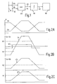
- Fig. 1 In the block diagram of Fig. 1 are on two lines 61 and 62 signals in Push differential, as shown in Fig. 2a with the voltage curves for the Signal voltages Ua and Ub is shown. These two signal voltages will be fed to a stage 64, the difference Ua - Ub of the two Signal voltages forms, which are output as signal voltage Uc on the line 65 becomes.
- the line 65 leads to a block 66, the inventive Contains circuitry and outputs with steep edges on the Line 67 generated. These are fed to a processing arrangement 68 which will not be explained in detail here, since it does not belong to the invention.
- the circuit arrangement according to the invention in block 66 is now constructed so that the signal on the line 67 already changes its value when the Signal voltage Uc exceeds a lower threshold V1. If the Signal voltage Uc an upper threshold V2 or even higher Threshold exceeds the switching threshold of the circuit in Block 66 is switched to the threshold V2, and thereby the signal changes on the line 67 its value at the falling edge of the signal voltage Uc, when the second threshold V2 is exceeded. In both cases, so early after the beginning of a change of the signal voltage Uc an output signal generated, so that a faster or earlier evaluation of the signal changes the lines 61 and 62 is possible.
- Fig. 2c the waveform of the signal voltage Uc is shown for the cases that the Line 61 or the line 62 is defective, for example by the relevant Line short to ground or to supply voltage has.
- Signal curve U'c is assumed that the voltage Ua is constantly high Potential or the voltage Ub is constantly at reference potential.
- the signal voltage U "c assumed that the voltage Ub constantly is at a high potential or the voltage Ua has constant reference potential. It is to recognize that the voltage U'c never crosses the lower threshold V1, so that constantly the upper threshold V2 remains effective. Run through accordingly the signal voltage U "c never exceeds the upper threshold V2, so that this constantly the lower threshold V1 remains effective. In both cases, so with the circuit according to the invention generates an output signal.
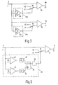
- FIG. 3 shows an embodiment of the circuit arrangement shown in FIG. 1 is indicated by the block 66.
- This circuit is used in this Example for generating three different values of the output signal, the two separate outputs 4a and 4b for each binary signal is delivered.
- One Signal input 2 for an input signal I is at a first input of two Comparators 6a and 6b are connected, which have a second input, with a switch 8a and 8b is connected.
- the output signal of the comparator 6a or 6b which is output at the output 4a or 4b, changes the binary State when the signal voltage at the first input of the relevant comparator the voltage at the second input exceeds or falls below.
- the second Input of the comparator 6a or 6b is dependent on the position of Switch 8a and 8b, a first threshold V1 or V'1 or a second Threshold V2 or V'2 supplied.
- the position of the switches 8a and 8b is by a switching device 10a or 10 b controlled, which has an input, which is also connected to the signal input 2 connected is.
- the switching device 10a which controls the changeover switch 8a, contains a Schmitt trigger 12a whose output signal from a first value to a second value changes when an upper threshold V3 is exceeded, and whose output signal assumes the first value again, if thereafter a lower one Switching threshold V4 is exceeded.
- a Schmitt trigger 12b whose output signal is the value changes if an upper switching threshold V'3 exceeded or a lower Switching threshold V'4 is exceeded.
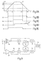
- Fig. 4a is an input signal with a linearly rising and falling edge shown. Go through these flanks different thresholds V1 to V4 and V'1 to V'4, respectively, in this example it is assumed that the threshold value V3 is equal to the threshold value V'4.
- the switches 8a and 8b are in the position shown in FIG Position.
- the comparators 6a and 6b give a low signal at the outputs 4a and 4b, if the input signal I below the threshold V1 or V'1 lies. If the input signal is the threshold V1 at time t1 exceeds the output O1 at the output 4a to a high value, as shown in Fig. 4b. If the input signal I is the threshold V2 goes through, a signal changes in the circuit of Fig. 3k. First if the threshold V3 is exceeded at the time t2, the Switching device 10a the switch 8a to the threshold value V2, as shown in FIG. 4c is shown. However, since threshold V2 is below threshold V3 is, the output signal O1 does not change its value.
- the output signal O2 of the comparator 6b goes to a high Value, as shown in Fig. 4d.
- the threshold value V'2 is exceeded there is again no signal change, while when exceeding the Threshold V'3 at time t4, the switching device 10b the switch 8b to the threshold V'2 switches.
- the output O2 of the comparator 6b does not change its value.
- the threshold value is reached at time t5 Go through V'2, and thus the output signal O2 goes back to a low Value. If, at the time t6, the threshold value V'4 is exceeded, switches the switching device 10b the switch 8b back to the lower threshold V'1 back. Because this threshold but above the input signal at Time t6 is located, the output signal O2 does not change.
- the threshold V2 is exceeded, and it works the output signal O1 back to a low value. Finally, the Time t8 the threshold V4 falls below, and thus switches the Switching device 10a the switch 8a back to the threshold V1. In order to the initial state is restored.
- the output signals O1 and O2 both in the rising edge as well as at the falling edge of the input signal I to Change the value at a relatively early stage.
- the threshold V'4 is here only for example equal to the threshold V3, in fact, can however, the thresholds V1 to V4 are arbitrarily opposite to the thresholds V'1 to be shifted to V'4 because they are independent of each other. It's easy too to see that the circuit of FIG. 3 by additional comparators and Switching devices can be extended if more than three different Output signals are to be generated. In the following description of the others Embodiments is assumed for the sake of simplicity that a Output signal with only two different values to be generated.
- FIG. 5 shows a circuit arrangement which likewise has a comparator 6 and a changeover switch 8, but in which the switching device 20 for the Switch 8 is constructed differently than in the circuit of Fig. 3.
- the Switching device 20 includes two comparators 22 and 24, each with a first Input, which is connected to the signal input 2 for the input signal I, and with a second input connected to the thresholds V3 and V4, respectively.
- the comparator 22 generates a high signal when the input signal I the Threshold V3 exceeds while comparator 24 only outputs a high signal generated when the input signal I is below the threshold V4, as by the circle at the output of the comparator 24 is indicated.
- the thresholds V1 to V4 are assumed as shown in FIG.
- the output of the comparator 22 is connected via a delay element 32 with a Input S of a flip-flop 26, while the output of the comparator 24th is connected to an input R of this flip-flop via a delay element 34.
- An output Q of the flip-flop 26 controls the switch 8.
- the input S is a high signal, and the output Q goes high and switches the switch 8 to the threshold V2, whereby the output signal 0 does not change.
- the signal at the input S the flip-flop 26 low again, but its state is maintained until the Signal falls below the threshold V4.
- the comparator 24 generates again a high signal, and the flip-flop 26 switches, causing the output Q to turn on low signal leads and the switch 8 back to the threshold V1 switches back.
- the output signal was 0 gone back to a low value.
- the switching device 20 in exactly behaves the same way as the switching device 10a of FIG. 3, when the Delays 32 and 34 are not taken into account. These cause that the flip-flop 26 is switched delayed, then the input voltage already higher than the threshold value V3 or a lower value than the threshold V4. This makes it possible for the Threshold voltage V3 only slightly greater than the threshold voltage V2 or even to choose the same. Accordingly, by the delay element 34, the Threshold voltage V4 only slightly lower than or equal to the Threshold voltage V1 can be selected. When both delay elements 32 and 34 They can also be used by a single dashed line Delay member 36 are replaced at the output of the flip-flop 26.
- Fig. 6 is not the Switched threshold voltage, but there are two comparators 42 and 44th provided, both of which are connected to the signal input 2 and of which the Comparator 42, the input signal with the threshold voltage V1 and the Comparator 44 compares the input signal with the threshold voltage V2.
- a changeover switch 48 which controls the signal output depending on the switch position with the output of the comparator 42 or the Comparator 44 connects.
- the switch 48 is controlled by a switching device 30th driven, in principle, in the same manner as the switching device 20 after Fig. 5 is constructed, only the delay elements are for clarity omitted.
- the sequence of Thresholds may be as indicated in the diagram of FIG. 4.
- First is the input signal I lower than the threshold value V4, so that the flip-flop 26th is brought into the reset state and the signal at the output Q low is and brings the switch in the drawn lower position. If that Input signal I exceeds the threshold V1, the signal is at the output of the comparator 42 and thus the output signal O at the signal output 4 high. If the input signal I thereafter exceeds the threshold value V2, so too the signal at the output of the comparator 44 is high, but this output is initially still open.
- circuit of FIG. 6 is the same Output signal generated as the circuit of FIG. 5.
- the difference in construction is that now two comparators 42 and 44 in addition to the Switching device 30 are used and that the switch with the outputs this comparator is connected.
- a significant Derive simplified circuit which is shown in Fig. 7.
- This contains one Comparator 52, of which one input to the signal input 2 and another Input is connected to the threshold V1. Further, a Schmitt trigger 54 present, which is also connected to the signal input 2 and the one Hysteresis between the thresholds V2 and V3 has. The output of the Comparator 52 and the Schmitt trigger 54 is connected to inputs of a changeover switch 48 connected, depending on the switch position, the output of one of these connects both elements with the signal output 4.
- the output of the comparator 52 is also via a delay element 50, here also by the circle has at the output indicated inverting function, with the input R of a Flip-flops 46 connected, and the output of the Schmitt trigger 54 is also with coupled to the input S of the flip-flop 46, wherein in this signal path also a Time delay element 50a may lie.
- the output Q of the flip-flop 46 controls the Switch 48.
- Fig. 8a is again the course of the input signal I and the location of thresholds V1, V2 and V3 are shown.
- the one with the before Threshold V4 used with the circuits described falls with the Threshold V1 together and is not specified separately.
- the input R of the flip-flop 46 receives a high signal and the flip-flop 46 in brings the reset position.
- the output Q has a low signal, so that the Switch 48 is in the drawn lower position.
- the signal at the output of the comparator 52 changes its value and becomes high, and thus also the output signal O at the signal output 4 becomes high, as shown in FIG. 8b and 8e is shown.
- the Schmitt carrier 54 outputs a high output Signal only when the input signal I is the threshold V3 at time t2 has exceeded, as shown in Fig. 8c.
- the flip-flop 46th switched immediately, if the delay element 50 does not exist, or delayed accordingly when the delay element 50a is present, as in Fig. 8d is shown.
- the output signal O at the signal output 4 changes its value is not, but remains high.
- the delay element 50 prevents the effect of small disturbances in the input signal I, because if at time t4, if the Threshold V1 is being traversed, small spurious signals on the Input signal I are present, the threshold value V1 a few times is exceeded and undershot, and corresponding signals then occur at the output of the comparator 52, as indicated in Fig. 8b. If that Delay element 50 would not exist at the first edge of the Signal at the output of the comparator 52, the flip-flop 46 tip over and the Changeover switch 48 to this output, so that the signal changes on Output of the comparator 52 would also appear at the signal output 4. By the delay element 50, the flip-flop 46 but only switched after These short signal changes at the output of the comparator 52 have decayed.
- the delay element 50 can be omitted, if comparator 52 is also used as a Schmitt carrier with a hysteresis between the threshold values V1 and V4 according to the sequence shown in FIG Thresholds is replaced.
- the Schmitt carrier 54 by be replaced by a simple comparator whose second input the Threshold V2 is obtained when the dashed line delay element 50a is available.
- the delay elements 50 and 50a may also be provided when the comparator 52 is executed as a Schmitt trigger to the Noise immunity of the circuit arrangement at both edges of the input signal in addition to increase.
- a circuit arrangement is shown, that of the circuit arrangement According to Fig. 7, when the switch 48 and the flip-flop 46 by individual Gates are realized.
- the output of the comparator 52 is connected to an input an AND gate 74 and an inverter 56 and a delay element 50 connected to an input of a NAND gate 70.
- the output of the Schmitt trigger 54 is connected to an input of an AND gate 76 and via a Delay member 50a is connected to an input of a NAND gate 72.
- the Outputs of NAND gates 70 and 72 are connected to another input of each other gate and with another input of the AND gate 74 and 76th connected.
- the outputs of the AND gates 74 and 76 lead to inputs of a OR gate 78 whose output is connected to the signal output 4.
- the NAND gates 70 and 72 form the flip-flop, while gates 74, 76 and 78 form the flip-flop Implement changeover switch.
- the function of the circuit of FIG. 9 is the same as FIG that of Fig. 7, as can
Description
Die Erfindung betrifft eine Schaltungsanordnung zum Erzeugen eines Ausgangssignals mit mehreren vorgegebenen Werten, die im wesentlichen übergangslos wechseln, aus einem sich wesentlich langsamer ändernden Eingangssignal.The invention relates to a circuit arrangement for generating a Output signal having a plurality of predetermined values, which is substantially change seamlessly, from a much slower changing Input signal.
Derartige Schaltungsanordnungen sind allgemein bekannt, beispielsweise aus dem Buch von Tietze/Schenk "Halbleiter-Schaltungsanordnungen", Springer-Verlag 1978, Seiten 134 und 135 sowie Seiten 412 bis 415 und dienen dazu, aus einem Eingangssignal mit langsamen Signalübergängen insbesondere eindeutige binäre Signale mit zwei Signalwerten zu erzeugen, die in logischen Schaltungen weiterverarbeitet werden können. Bei einer solchen Schaltung wechselt das Ausgangssignal seinen Wert, wenn das Eingangssignal einen hohen Schwellenwert überschreitet, und das Ausgangssignal kehrt wieder auf seinen vorhergehenden Wert zurück, wenn das Eingangssignal danach einen niedrigeren Schwellenwert unterschreitet. Auf diese Weise wird erreicht, daß das Ausgangssignal nicht von eventuellen kleinen Störsignalen, die dem Eingangssignal überlagert sind, beeinflußt wird. Wenn nämlich das Eingangssignal den oberen Schwellenwert überschritten hat, kann nur ein negatives Störsignal, das das Eingangssignal unter den unteren Schwellenwert bringt, eine Änderung des Ausgangssignals erzeugen, und umgekehrt bei der Rückflanke des Eingangssignals.Such circuits are well known, for example from the Book by Tietze / Schenk "Halbleiter-Schaltungsanordnungen", Springer-Verlag 1978, Pages 134 and 135 as well as pages 412 to 415 and serve to one from Input signal with slow signal transitions, in particular unique binary To generate signals with two signal values, which are in logic circuits can be further processed. In such a circuit that changes Output signal its value when the input signal has a high threshold exceeds, and the output signal returns to its previous value back if the input signal thereafter a lower threshold below. In this way it is achieved that the output signal is not from any small interfering signals which are superimposed on the input signal influenced becomes. Namely, if the input signal exceeded the upper threshold has, can only have a negative noise signal, which is the input signal below the bottom Threshold, produce a change in the output signal, and vice versa at the trailing edge of the input signal.
Nachteilig ist bei den bekannten Schaltungen, daß die Auswertung des Signals erst relativ spät nach Beginn der ansteigenden oder abfallenden Flanke möglich ist. Wenn die Eingangssignale von einem Bus kommen, an dem mehrere Geräte angeschlossen sind, von denen jedes Gerät die Übertragung einer Nachricht auslösen kann (Multimaster-Betrieb), wird zur Vermeidung von Konflikten auf dem Bus jedes Signal eine vorgegebene Zeit nach dem Beginn der Vorderflanke des Signals abgetastet und nur der Signalzustand bei der Abtastung ausgewertet. Bei einem räumlich ausgedehnten Bus können die Signalflanken relativ flach sein, so daß die Dauer jedes Signals einen bestimmten Wert nicht unterschreiten darf. Dadurch wird die maximale Frequenz der Signale und damit Übertragungskapazität auf dem Bus beschränkt. Außerdem ist bei den bekannten Schaltungen erforderlich, daß das Eingangssignal sowohl den höheren Schwellenwert überschreitet als auch den niedrigeren Schwellenwert unterschreitet. Wenn das Eingangssignal jedoch von der Signaldifferenz auf zwei Leitungen, die ein Signal im Gegentakt übertragen, abgeleitet wird und beispielsweise eine dieser beiden Leitungen durch ein Leitungsfehler ständig ein hohes oder ein niedriges Signal überträgt, ändert sich das davon abgeleitete Eingangssignal mit einem kleineren Hub nur im unteren oder nur im oberen Wertebereich, so daß in diesem Falle mittels bekannter Schaltungsanordnungen nur schwierig ein brauchbares Ausgangssignal erhalten werden kann.A disadvantage of the known circuits that the evaluation of the signal only relatively late after the beginning of the rising or falling edge is possible. When the input signals come from a bus that has multiple devices are connected, each device triggering the transmission of a message can (multi-master operation), to avoid conflicts on the bus each Signal a predetermined time after the beginning of the leading edge of the signal sampled and evaluated only the signal state during the scan. At a spatially extended bus, the signal edges can be relatively flat, so that the Duration of each signal must not fall below a certain value. This will the maximum frequency of the signals and thus transmission capacity on the bus limited. In addition, it is necessary in the known circuits that the Input signal exceeds both the higher threshold and the lower threshold. However, if the input signal from the Signal difference on two lines that transmit a signal in push-pull, is derived and, for example, one of these two lines by a Line fault constantly transmits a high or a low signal, this changes derived input signal with a smaller stroke only in the lower or only in the upper range, so that in this case by means of known Circuit arrangements difficult to obtain a useful output signal can be.
Aufgabe der Erfindung ist es, eine Schaltungsanordnung der eingangs genannten Art anzugeben, die eine möglichst schnelle Auswertung einer Eingangssignaländerung ermöglicht und die auch bei Eingangssignalen mit einem geringeren Hub und einem Offset in der Größenordnung dieses geringeren Signalhubs noch weitgehend zuverlässig arbeitet.The object of the invention is a circuit arrangement of the type mentioned specify the fastest possible evaluation of an input signal change allows and also with input signals with a lower stroke and a Offset in the order of magnitude of this lower signal swing still largely works reliably.
Diese Aufgabe wird erfindungsgemäß dadurch gelöst, daß der Schwellenwert, bei dem das Ausgangssignal den Wert wechselt, bei der ansteigenden Flanke des Eingangssignals niedrig und bei der abfallenden Flanke des Eingangssignals hoch ist. Die Umschaltung zwischen diesen beiden Schwellenwerten wird abhängig vom Eingangssignal durchgeführt, und zwar bei weiteren Schwellenwerten, die unterschiedlich zu den erstgenannten Schwellenwerten sein können. Die Umschaltung auf den höheren Schwellenwert erfolgt, wenn die ansteigende Flanke des Eingangssignals mindestens diesen höheren Schwellenwert überschritten hat, und die Rückschaltung auf den niedrigeren Schwellenwert erfolgt, wenn bei der abfallenden Flanke des Eingangssignals wenigstens dieser niedrigere Schwellenwert unterschritten wird. Der Wechsel des Ausgangssignals kann dabei früher erfolgen als bei bekannten Schaltungen, nämlich kurz nach dem Beginn der ansteigenden bzw. der abfallenden Flanke. Eine zwangsläufige Folge dieser Maßnahme ist allerdings, daß der Störabstand zumindest für bestimmte Störsignale verringert wird. Dies wird dadurch kompensiert, daß in bekannter Weise das Eingangsignal eine bestimmte Zeitspanne nach dem ersten Wechsel des Ausgangssignals abgetastet wird.This object is achieved in that the threshold at the output signal changes the value at the rising edge of the Input signal is low and high at the falling edge of the input signal. Switching between these two thresholds will depend on the Input signal carried out, and in other thresholds, the different from the first mentioned thresholds. The Switching to the higher threshold occurs when the rising edge of the input signal has exceeded at least this higher threshold, and the switch back to the lower threshold occurs when at the falling edge of the input signal at least this lower threshold is fallen short of. The change of the output signal can be done earlier than in known circuits, namely shortly after the beginning of the rising or the falling edge. An inevitable consequence of this measure, however, is that the signal-to-noise ratio is reduced, at least for certain interference signals. this will compensated in that, in a known manner, the input signal a certain Time interval is scanned after the first change of the output signal.
Das erfindungsgemäße Prinzip läßt sich auch anwenden, wenn das Ausgangssignal nicht binär ist, sondern mehr als zwei Werte annehmen kann. Dafür sind dann entsprechend mehr Schwellenwerte erforderlich. Die Umschaltung der Schaltschwelle vom unteren oder ersten Schwellenwert auf den oberen oder zweiten Schwellenwert kann erfolgen, wenn das Eingangssignal einen dritten Schwellenwert überschritten hat, der größer als oder gleich dem zweiten Schwellenwert sein kann, und entsprechend kann die Umschaltung der Schaltschwelle auf den ersten Schwellenwert erfolgen, wenn das Eingangssignal einen vierten Schwellenwert unterschritten hat, der gleich oder niedriger als der erste Schwellenwert ist. Bei Gleichheit der Schwellenwerte kann eine größere Unempfindlichkeit gegen Strörsignale erreicht werden, wenn die Umschaltung nach Erreichen des entsprechenden Schwellenwertes verzögert erfolgt.The principle of the invention can also be applied if the output signal is not binary, but can take more than two values. That's what then correspondingly more thresholds required. Switching the Switching threshold from the lower or first threshold to the upper or second threshold Threshold can occur when the input signal has a third threshold exceeded, which may be greater than or equal to the second threshold, and accordingly, the switching of the switching threshold to the first Threshold occur when the input signal has a fourth threshold is less than or equal to the first threshold. at Equality of thresholds can be greater insensitivity to Strörsignale be achieved when switching after reaching the corresponding threshold is delayed.
Eine konkrete Ausführung von der erfindungsgemäßen Schaltungsanordnung kann darin bestehen, daß zur Erzeugung des Ausgangssignals ein Vergleicher verwendet wird, der das Eingangssignal mit einem Schwellenwert vergleicht und bei Gleichheit den Wert des Ausgangssignals wechselt, wobei der Schwellenwert durch eine zusätzliche Schalteinrichtung abhängig vom Eingangssignal umgeschaltet wird. Wenn der Vergleicher bei dem jeweiligen Schwellenwert eine Schalthysterese aufweist, wird die Empfindlichkeit gegenüber Störsignalen im Eingangssignal verringert. A concrete embodiment of the circuit arrangement according to the invention can be that used to generate the output signal, a comparator which compares the input signal to a threshold and equality the value of the output signal changes, the threshold by a additional switching device is switched depending on the input signal. If the comparator at the respective threshold, a switching hysteresis has the sensitivity to noise in the input signal reduced.
Bei einer anderen Ausführungsform der erfindungsgemäßen Schaltungsanordnung werden zwei Vergleicher verwendet, von denen der eine das Eingangsignal mit dem ersten Schwellenwert und der andere mit dem zweiten Schwellenwert vergleicht. Die Ausgänge der beiden Vergleicher führen auf einen Umschalter, der abhängig vom dritten bzw. vierten Schwellenwert umgeschaltet wird und damit das Ausgangssignal von dem Ausgang des einen oder des anderen Vergleichers abnimmt. Dies wirkt in genau gleicher Weise wie die Umschaltung des Schwellenwertes bei Verwendung nur eines Vergleichers für den ersten und zweiten Schwellenwert. Auch in diesem Falle können die beiden Vergleicher oder wenigstens einer davon eine Schalthysterese aufweisen, um die Empfindlichkeit gegenüber Störsignale im Eingangsignal zu verringern.In another embodiment of the circuit arrangement according to the invention Two comparators are used, one of which is the input signal with the first threshold and the other compares to the second threshold. The Outputs of the two comparators lead to a switch, which depends on third or fourth threshold value is switched, and thus the output signal decreases from the output of one or the other comparator. This works in exactly the same as the switching of the threshold value in use only one comparator for the first and second thresholds. Also in this Traps may be the two comparators or at least one of them Have switching hysteresis to reduce the sensitivity to noise in Reduce input signal.
Die Umschaltung des Schwellenwertes bei Verwendung eines Vergleichers oder des Ausgangssignals bei Verwendung von zwei Vergleichern erfolgt mit Hilfe einer Schalteinrichtung, die vom Eingangssignal gesteuert wird. Diese kann einen Schwellwertschalter mit Hysterese enthalten, wobei die Umschaltpunkte gleich dem dritten bzw. dem vierten Schwellenwert sind. Es kann aber auch für jeden dieser beiden Schwellenwerte ein eigener Vergleicher verwendet werden, und beide Vergleicher steuern eine Speicherstufe, deren Ausgangssignal die Umschaltung bewirkt. Bei der letztgenannten Ausführungsform und der Verwendung von zwei Vergleichern für das Erzeugen des Ausgangssignals können außerdem die Signale an den Ausgängen dieser Vergleicher direkt zur Steuerung der Speicherstufe verwendet werden. Dies ergibt einen besonders einfachen Aufbau.Switching the threshold value when using a comparator or the Output signal when using two comparators is done with the help of a Switching device controlled by the input signal. This one can Threshold switch with hysteresis included, where the switching points equal to the third and fourth threshold, respectively. But it can also be for each of these Both thresholds can be used a separate comparator, and both Comparators control a memory stage whose output is the switchover causes. In the latter embodiment and the use of two Comparators for generating the output signal may also be the signals to The outputs of these comparators are used directly to control the memory level become. This results in a particularly simple structure.
Ausführungsbeispiele der Erfindung werden nachfolgend anhand der Zeichnung
näher erläutert. Es zeigen
In dem Blockschaltbild der Fig. 1 werden auf zwei Leitungen 61 und 62 Signale im
Gegentakt übertragen, wie in Fig. 2a mit den Spannungsverläufen für die
Signalspannungen Ua und Ub dargestellt ist. Diese beiden Signalspannungen werden
einer Stufe 64 zugeführt, die daraus die Differenz Ua - Ub der beiden
Signalspannungen bildet, die als Signalspannung Uc auf der Leitung 65 abgegeben
wird. Die Leitung 65 führt auf einen Block 66, der die erfindungsgemäße
Schaltungsanordnung enthält und Ausgangssignale mit steilen Flanken auf der
Leitung 67 erzeugt. Diese werden einer Verarbeitungsanordnung 68 zugeführt, die
hier nicht näher erläutert wird, da sie nicht zur Erfindung gehört.In the block diagram of Fig. 1 are on two
Der Verlauf der Signalspannung Uc = Ua - Ub und der Spannung auf der Leitung
67 sind in Fig. 2b dargestellt. Die Spannung Uc, die das Eingangssignal für der
Block 66 bildet, geht hier von negativen zu positiven Werten, jedoch ist klar, daß
durch eine entsprechenden Spannungsverschiebung auch nur positive Werte für die
Signalspannung Uc erzeugt werden können.The course of the signal voltage Uc = Ua - Ub and the voltage on the
Die erfindungsgemäße Schaltungsanordnung im Block 66 ist nun so aufgebaut, daß
das Signal auf der Leitung 67 seinen Wert bereits wechselt, wenn die
Signalspannung Uc einen unteren Schwellenwert V1 überschreitet. Wenn die
Signalspannung Uc einen oberen Schwellenwert V2 oder einen noch höheren
Schwellenwert überschreitet, wird die Schaltschwelle der Schaltungsanordnung im
Block 66 auf den Schwellenwert V2 umgeschaltet, und dadurch wechselt das Signal
auf der Leitung 67 seinen Wert bei der abfallenden Flanke der Signalspannung Uc,
wenn der zweite Schwellenwert V2 unterschritten wird. In beiden Fällen wird also
frühzeitig nach Beginn einer Änderung der Signalspannung Uc ein Ausgangssignal
erzeugt, so daß eine schnellere bzw. frühere Auswertung der Signaländerungen auf
den Leitungen 61 und 62 möglich ist.The circuit arrangement according to the invention in
In Fig. 2c ist der Verlauf der Signalspannung Uc für die Fälle dargestellt, daß die
Leitung 61 oder die Leitung 62 defekt ist, beispielsweise indem die betreffende
Leitung Kurzschluß gegen Masse oder gegen Versorgungsspannung hat. Bei dem
Signalverlauf U'c ist angenommen, daß die Spannung Ua ständig auf hohem
Potential oder die Spannung Ub ständig auf Bezugspotential liegt. Entsprechend ist
für den Verlauf der Signalspannung U"c angenommen, daß die Spannung Ub ständig
auf hohem Potential liegt oder die Spannung Ua ständig Bezugspotential hat. Es ist
zu erkennen, daß die Spannung U'c niemals den unteren Schwellenwert V1 kreuzt,
so daß ständig der obere Schwellenwert V2 wirksam bleibt. Entsprechend durchläuft
die Signalspannung U"c niemals den oberen Schwellenwert V2, so daß hierfür
ständig der untere Schwellenwert V1 wirksam bleibt. In beiden Fällen wird also mit
der erfindungsgemäßen Schaltung ein Ausgangssignal erzeugt.In Fig. 2c, the waveform of the signal voltage Uc is shown for the cases that the
In Fig. 3 ist eine Ausführungsform der Schaltungsanordnung dargestellt, die in Fig.
1 durch den Block 66 angedeutet ist. Diese Schaltungsanordnung dient in diesem
Beispiel zur Erzeugung von drei verschiedenen Werten des Ausgangssignals, das an
zwei getrennten Ausgängen 4a und 4b für je ein binäres Signal abgegeben wird. Ein
Signaleingang 2 für ein Eingangsignal I ist mit einem ersten Eingang von zwei
Vergleichern 6a und 6b verbunden, die einen zweiten Eingang aufweisen, der mit
einem Umschalter 8a bzw. 8b verbunden ist. Das Ausgangssignal der Vergleicher 6a
bzw. 6b, das am Ausgang 4a bzw. 4b abgegeben wird, wechselt den binären
Zustand, wenn die Signalspannung am ersten Eingang des betreffenden Vergleichers
die Spannung am zweiten Eingang überschreitet bzw. unterschreitet. Dem zweiten
Eingang der Vergleicher 6a bzw. 6b wird abhängig von der Stellung des
Umschalters 8a bzw. 8b ein ersten Schwellenwert V1 bzw. V'1 oder ein zweiter
Schwellenwert V2 bzw. V'2 zugeführt.FIG. 3 shows an embodiment of the circuit arrangement shown in FIG.
1 is indicated by the
Die Stellung der Umschalter 8a und 8b wird durch eine Schalteinrichtung 10a bzw.
10b gesteuert, die einen Eingang aufweist, der ebenfalls mit dem Signaleingang 2
verbunden ist. Die Schalteinrichtung 10a, die den Umschalter 8a steuert, enthält
einen Schmitt-Trigger 12a, dessen Ausgangssignal von einem ersten Wert auf einen
zweiten Wert wechselt, wenn eine obere Schaltschwelle V3 überschritten wird, und
dessen Ausgangssignal den ersten Wert wieder annimmt, wenn danach eine untere
Schaltschwelle V4 unterschritten wird. In entsprechender Weise enthält die
Schalteinrichtung 10b einen Schmitt-Trigger 12b, dessen Ausgangssignal den Wert
wechselt, wenn eine obere Schaltschwelle V'3 überschritten bzw. eine untere
Schaltschwelle V'4 unterschritten wird.The position of the
Die Funktion der in Fig. 3 dargestellten Schaltungsanordnung soll anhand des Diagramms in Fig. 4 erläutert werden. In Fig. 4a ist ein Eingangssignal mit einer linear ansteigenden und abfallenden Flanke dargestellt. Diese Flanken durchlaufen verschiedene Schwellenwerte V1 bis V4 bzw. V'1 bis V'4, wobei in diesem Beispiel angenommen ist, daß der Schwellenwert V3 gleich dem Schwellenwert V'4 ist.The function of the circuit arrangement shown in Fig. 3 is based on the Diagram are explained in Fig. 4. In Fig. 4a is an input signal with a linearly rising and falling edge shown. Go through these flanks different thresholds V1 to V4 and V'1 to V'4, respectively, in this example it is assumed that the threshold value V3 is equal to the threshold value V'4.
Zu Beginn befinden sich die Umschalter 8a und 8b in der in Fig. 3 dargestellten
Stellung. Die Vergleicher 6a und 6b geben ein niedriges Signal an den Ausgängen
4a bzw. 4b ab, wenn das Eingangssignal I unter dem Schwellenwert V1 bzw. V'1
liegt. Wenn das Eingangssignal den Schwellenwert V1 zum Zeitpunkt t1
überschreitet, geht das Ausgangssignal O1 am Ausgang 4a auf einen hohen Wert,
wie in Fig. 4b dargestellt ist. Wenn das Eingangssignal I den Schwellenwert V2
durchläuft, ändert sich in der Schaltungsanordnung nach Fig. 3k ein Signal. Erst
wenn zum Zeitpunkt t2 der Schwellenwert V3 überschritten wird, schaltet die
Schalteinrichtung 10a den Umschalter 8a auf den Schwellenwert V2 um, wie in Fig.
4c dargestellt ist. Da der Schwellenwert V2 jedoch unter dem Schwellenwert V3
liegt, ändert das Ausgangssignal O1 nicht seinen Wert.Initially, the
Wenn danach das Eingangssignal I zum Zeitpunkt t3 den Schwellenwert V'1
überschreitet, geht das Ausgangssignal O2 des Vergleichers 6b auf einen hohen
Wert, wie in Fig. 4d dargestellt ist. Beim Überschreiten des Schwellenwertes V'2
gibt es wieder keine Signaländerung, während beim Überschreiten des
Schwellenwertes V'3 zum Zeitpunkt t4 die Schalteinrichtung 10b den Umschalter 8b
auf den Schwellenwert V'2 umschaltet. Das Ausgangssignal O2 des Vergleichers 6b
ändert dadurch seinen Wert nicht.After that, the input signal I at time t3 the threshold value V'1
exceeds, the output signal O2 of the
Wenn das Eingangssignal I wieder abfällt, wird zum Zeitpunkt t5 der Schwellenwert
V'2 durchlaufen, und damit geht das Ausgangssignal O2 wieder auf einen niedrigen
Wert. Wenn zum Zeitpunkt t6 der Schwellenwert V'4 unterschritten wird, schaltet
die Schalteinrichtung 10b den Umschalter 8b wieder auf den unteren Schwellenwert
V'1 zurück. Da dieser Schwellenwert aber oberhalb des Eingangssignals beim
Zeitpunkt t6 liegt, ändert sich das Ausgangssignal O2 nicht.When the input signal I falls again, the threshold value is reached at time t5
Go through V'2, and thus the output signal O2 goes back to a low
Value. If, at the time t6, the threshold value V'4 is exceeded, switches
the
Zum Zeitpunkt t7 wird der Schwellenwert V2 unterschritten, und damit geht auch das Ausgangssignal O1 wieder auf einen niedrigen Wert. Schließlich wird zum Zeitpunkt t8 der Schwellenwert V4 unterschritten, und damit schaltet die Schalteinrichtung 10a den Umschalter 8a wieder auf den Schwellenwert V1. Damit ist der Anfangszustand wieder hergestellt.At time t7, the threshold V2 is exceeded, and it works the output signal O1 back to a low value. Finally, the Time t8 the threshold V4 falls below, and thus switches the Switching device 10a the switch 8a back to the threshold V1. In order to the initial state is restored.
Aus Fig. 4 ist zu erkennen, daß die Ausgangssignale O1 und O2 sowohl bei der ansteigenden Flanke als auch bei der abfallenden Flanke des Eingangssignals I zu einem relativ frühen Zeitpunkt den Wert wechseln. Der Schwellenwert V'4 ist hier nur beispielsweise gleich dem Schwellenwert V3 angenommen, tatsächlich können jedoch die Schwellenwerte V1 bis V4 beliebig gegenüber den Schwellenwerten V'1 bis V'4 verschoben sein, da sie voneinander unabhängig sind. Es ist auch leicht einzusehen, daß die Schaltung nach Fig. 3 durch zusätzliche Vergleicher und Schalteinrichtungen erweitert werden kann, wenn mehr als drei verschiedene Ausgangssignale erzeugt werden sollen. In der folgenden Beschreibung der weiteren Ausführungsbeispiele wird der Einfachheit halber davon ausgegangen, daß ein Ausgangssignal mit nur zwei verschiedenen Werten erzeugt werden soll.From Fig. 4 it can be seen that the output signals O1 and O2 both in the rising edge as well as at the falling edge of the input signal I to Change the value at a relatively early stage. The threshold V'4 is here only for example equal to the threshold V3, in fact, can however, the thresholds V1 to V4 are arbitrarily opposite to the thresholds V'1 to be shifted to V'4 because they are independent of each other. It's easy too to see that the circuit of FIG. 3 by additional comparators and Switching devices can be extended if more than three different Output signals are to be generated. In the following description of the others Embodiments is assumed for the sake of simplicity that a Output signal with only two different values to be generated.
In Fig. 5 ist eine Schaltungsanordnung dargestellt, die ebenfalls einen Vergleicher 6
und einen Umschalter 8 aufweist, bei der jedoch die Schalteinrichtung 20 für den
Umschalter 8 anders aufgebaut ist als bei der Schaltung nach Fig. 3. Die
Schalteinrichtung 20 enthält zwei Vergleicher 22 und 24 mit je einem ersten
Eingang, der mit dem Signaleingang 2 für das Eingangssignal I verbunden ist, und
mit einem zweiten Eingang, der mit dem Schwellenwert V3 bzw. V4 verbunden ist.
Der Vergleicher 22 erzeugt ein hohes Signal, wenn das Eingangssignal I den
Schwellenwert V3 überschreitet, während der Vergleicher 24 ein hohes Signal nur
erzeugt, wenn das Eingangssignal I unter dem Schwellenwert V4 liegt, wie durch
den Kreis am Ausgang des Vergleichers 24 angedeutet ist. Die Schwellenwerte V1
bis V4 werden wie in Fig. 4 dargestellt angenommen.FIG. 5 shows a circuit arrangement which likewise has a
Der Ausgang des Vergleichers 22 ist über ein Verzögerungsglied 32 mit einem
Eingang S eines Flipflops 26 verbunden, während der Ausgang des Vergleichers 24
mit einem Eingang R dieses Flipflops über ein Verzögerungsglied 34 verbunden ist.
Ein Ausgang Q des Flipflops 26 steuert den Umschalter 8.The output of the
Wenn zu Beginn das Eingangssignal I unter dem Schwellenwert V4 liegt, erhält das
Flipflop 26 am Eingang R ein hohes Signal, so daß am Ausgang Q ein niedriges
Signal abgegeben wird und der Umschalter 8 mit dem Schwellenwert V1 verbunden
ist. Wenn das Eingangssignal I danach den Schwellenwert V4 überschreitet, wird
das Signal am Eingang R des Flipflops 26 niedrig, jedoch bleibt dessen Zustand
erhalten und der Ausgang Q niedrig und die Stellung des Umschalters 8
unverändert. Beim Überschreiten des Schwellenwertes V1 schaltet der Vergleicher 6
das Ausgangssignal 0 am Signalausgang 4 auf einen hohen Wert. Der Zustand des
Flipflops 26 bleibt unverändert, bis das Eingangssignal I den Schwellenwert V3
überschreitet. In diesem Augenblick erhält, wenn zunächst der Einfluß des
Verzögerungsglieds 32 nicht berücksichtigt wird, der Eingang S ein hohes Signal,
und der Ausgang Q wird hoch und schaltet den Umschalter 8 auf den Schwellenwert
V2, wodurch sich das Ausgangssignal 0 nicht ändert. Wenn danach das
Eingangssignal I unter den Schwellenwert V3 fällt, wird das Signal am Eingang S
des Flipflops 26 wieder niedrig, jedoch bleibt dessen Zustand erhalten, bis das
Signal unter den Schwellenwert V4 fällt. Dann erzeugt der Vergleicher 24 wieder
ein hohes Signal, und das Flipflop 26 schaltet um, wodurch der Ausgang Q ein
niedriges Signal führt und den Umschalter 8 wieder auf den Schwellenwert V1
zurück schaltet. Beim Durchlaufen des Schwellenwertes 2 war das Ausgangssignal 0
wieder auf einen niedrigen Wert gegangen.If, at the beginning, the input signal I is below the threshold value V4, this receives
Flip-
Aus dieser Beschreibung ist zu erkennen, daß sich die Schalteinrichtung 20 in genau
gleicher Weise verhält wie die Schalteinrichtung 10a nach Fig. 3, wenn die
Verzögerungsglieder 32 und 34 nicht berücksichtigt werden. Diese bewirken, daß
das Flipflop 26 verzögert umgeschaltet wird, wobei dann die Eingangsspannung
bereits einen höheren Wert als den Schwellenwert V3 bzw. einen niedrigeren Wert
als den Schwellenwert V4 angenommen hat. Dadurch ist es möglich, die
Schwellenspannung V3 nur wenig größer als die Schwellenspannung V2 oder sogar
gleich dieser zu wählen. Entsprechend kann durch das Verzögerungsglied 34 die
Schwellenspannung V4 nur wenig niedriger als die oder gleich der
Schwellenspannung V1 gewählt werden. Wenn beide Verzögerungsglieder 32 und 34
verwendet werden, können sie auch durch ein einziges, gestrichelt dargestelltes
Verzögerungsglied 36 am Ausgang des Flipflops 26 ersetzt werden. From this description it can be seen that the switching
Bei dem in Fig. 6 dargestellten Ausführungsbeispiel wird nicht die
Schwellenspannung umgeschaltet, sondern es sind zwei Vergleicher 42 und 44
vorgesehen, die beide mit dem Signaleingang 2 verbunden sind und von denen der
Vergleicher 42 das Eingangssignal mit der Schwellenspannung V1 und der
Vergleicher 44 das Eingangssignal mit der Schwellenspannung V2 vergleicht. Der
Signalausgang 4 ist hier mit einem Umschalter 48 verbunden, der den Signalausgang
abhängig von der Schalterstellung mit dem Ausgang des Vergleichers 42 oder des
Vergleichers 44 verbindet. Der Umschalter 48 wird von einer Schalteinrichtung 30
angesteuert, die grundsätzlich in gleicher Weise wie die Schalteinrichtung 20 nach
Fig. 5 aufgebaut ist, lediglich die Verzögerungsglieder sind der Übersichtlichkeit
halber weggelassen.In the embodiment shown in Fig. 6 is not the
Switched threshold voltage, but there are two
Die Funktion der Schaltung nach Fig. 6 ist wie folgt, wobei die Folge der
Schwellenwerte wie in dem Diagramm nach Fig. 4 angegeben sein möge. Zunächst
ist das Eingangssignal I niedriger als der Schwellenwert V4, so daß das Flipflop 26
in den rückgesetzten Zustand gebracht wird und das Signal am Ausgang Q niedrig
ist und den Schalter in die gezeichnete untere Stellung bringt. Wenn das
Eingangssignal I den Schwellenwert V1 überschreitet, wird das Signal am Ausgang
des Vergleichers 42 und damit das Ausgangssignal O am Signalausgang 4 hoch.
Wenn das Eingangssignal I danach den Schwellenwert V2 überschreitet, wird auch
das Signal am Ausgang des Vergleichers 44 hoch, jedoch ist dieser Ausgang
zunächst noch offen.The function of the circuit of FIG. 6 is as follows, the sequence of
Thresholds may be as indicated in the diagram of FIG. 4. First
is the input signal I lower than the threshold value V4, so that the flip-flop 26th
is brought into the reset state and the signal at the output Q low
is and brings the switch in the drawn lower position. If that
Input signal I exceeds the threshold V1, the signal is at the output
of the
Beim Überschreiten des Schwellenwertes V3 wird das Flipflop 26 durch den
Vergleicher 22 in der Schalteinrichtung 30 umgeschaltet, und damit geht der
Umschalter 48 in die obere Stellung, wodurch sich das Ausgangssignal O jedoch
nicht ändert.When the threshold V3 is exceeded, the flip-
Wenn danach das Eingangssignal I den Schwellenwert V2 unterschreitet, wird das
Signal am Ausgang des Vergleichers 44 und damit das Ausgangssignal O am
Signalausgang 4 niedrig. Das Signal am Ausgang des Vergleichers 42 ist jedoch
noch zunächst hoch, und es wird erst niedrig, wenn das Eingangssignal I den
Schwellenwert V1 unterschritten hat. Wenn danach auch der Schwellenwert V4
unterschritten wird, schaltet das Flipflop 26 wieder in den Anfangszustand zurück,
so daß der Umschalter 48 wieder in die untere Stellung geschaltet wird. Das
Ausgangssignal O ändert sich dabei nicht, sondern bleibt niedrig.Thereafter, when the input signal I falls below the threshold V2, the
Signal at the output of the
Aus dieser Beschreibung ist zu erkennen, daß die Schaltung nach Fig. 6 das gleiche
Ausgangssignal erzeugt wie die Schaltung nach Fig. 5. Der Unterschied im Aufbau
besteht darin, daß nun zwei Vergleicher 42 und 44 zusätzlich zu der
Schalteinrichtung 30 verwendet werden und daß der Umschalter mit den Ausgängen
dieser Vergleicher verbunden ist.From this description it can be seen that the circuit of FIG. 6 is the same
Output signal generated as the circuit of FIG. 5. The difference in construction
is that now two
Aus den bisher beschriebenen Ausführungsbeispielen läßt sich eine wesentlich
vereinfachte Schaltung ableiten, die in Fig. 7 dargestellt ist. Diese enthält einen
Vergleicher 52, von dem ein Eingang mit dem Signaleingang 2 und ein weiterer
Eingang mit dem Schwellenwert V1 verbunden ist. Ferner ist ein Schmitt-Trigger 54
vorhanden, der ebenfalls mit den Signaleingang 2 verbunden ist und der eine
Hysterese zwischen den Schwellenwerten V2 und V3 aufweist. Der Ausgang des
Vergleichers 52 und des Schmitt-Triggers 54 ist mit Eingängen eines Umschalters
48 verbunden, der abhängig von der Schalterstellung den Ausgang eines dieser
beiden Elemente mit dem Signalausgang 4 verbindet. Der Ausgang des Vergleichers
52 ist außerdem über ein Verzögerungsglied 50, das hier auch eine durch den Kreis
am Ausgang angedeutete invertierende Funktion hat, mit dem Eingang R eines
Flipflops 46 verbunden, und der Ausgang des Schmitt-Triggers 54 ist außerdem mit
dem Eingang S des Flipflops 46 gekoppelt, wobei in diesem Signalweg ebenfalls ein
Zeitverzögerungsglied 50a liegen kann. Der Ausgang Q des Flipflops 46 steuert den
Umschalter 48. From the embodiments described so far, a significant
Derive simplified circuit, which is shown in Fig. 7. This contains one
Bei der Schaltung nach Fig. 7 bildet lediglich das Flipflop 46 eine Schalteinrichtung
40, die die Stellung des Umschalters 48 steuert. Gegenüber den Schaltungen nach
Fig. 5 und Fig. 6 sind die Vergleicher 22 und 24 weggelassen, da deren Funktion
durch den Vergleicher 52 bzw. den Schmitt-Trigger 54 übernommen ist.In the circuit of FIG. 7, only the flip-
Die Funktion der Schaltung nach Fig. 7 soll anhand des in Fig. 8 dargestellten
Diagramms erläutert werden. In Fig. 8a ist wieder der Verlauf des Eingangssignals I
und die Lage der Schwellenwerte V1, V2 und V3 dargestellt. Der bei den vorher
beschriebenen Schaltungen verwendete Schwellenwert V4 fällt mit dem
Schwellenwert V1 zusammen und ist nicht gesondert angegeben. Zunächst ist das
Signal am Ausgang des Vergleichers 52 und auch des Schmitt-Triggers 54 niedrig,
so daß der Eingang R des Flipflops 46 ein hohes Signal erhält und das Flipflop 46 in
die rückgesetzte Stellung bringt. Der Ausgang Q hat ein niedriges Signal, so daß der
Umschalter 48 in der gezeichneten unteren Stellung steht.The function of the circuit according to FIG. 7 will be described with reference to FIG
Diagram explained. In Fig. 8a is again the course of the input signal I
and the location of thresholds V1, V2 and V3 are shown. The one with the before
Threshold V4 used with the circuits described falls with the
Threshold V1 together and is not specified separately. At first that is
Signal at the output of the
Wenn das Eingangssignal I den Schwellenwert V1 zum Zeitpunkt t1 überschreitet,
wechselt das Signal am Ausgang des Vergleichers 52 seinen Wert und wird hoch,
und damit wird auch das Ausgangssignal O am Signalausgang 4 hoch, wie in Fig.
8b bzw. Fig. 8e dargestellt ist. Der Schmitt-Träger 54 gibt am Ausgang ein hohes
Signal erst ab, wenn das Eingangssignal I den Schwellenwert V3 zum Zeitpunkt t2
überschritten hat, wie in Fig. 8c dargestellt ist. Damit wird das Flipflop 46
umgeschaltet, und zwar sofort, wenn das Verzögerungsglied 50 nicht vorhanden ist,
bzw. entsprechend verzögert, wenn das Verzögerungsglied 50a vorhanden ist, wie in
Fig. 8d dargestellt ist. Das Ausgangssignal O am Signalausgang 4 ändert dabei
seinen Wert nicht, sondern bleibt hoch.If the input signal I exceeds the threshold value V1 at time t1,
the signal at the output of the
Wenn danach das Eingangssignal I wieder abfällt und den Schwellenwert V2 zum
Zeitpunkt t3 unterschreitet, wird das Signal am Ausgang des Schmitt-Triggers 54
wieder niedrig und damit wird auch das Ausgangssignal O niedrig, da der Schalter
48 noch in der oberen Stellung steht. Wenn danach das Eingangssignal I zum
Zeitpunkt t4 den Schwellenwert V1 unterschreitet, wird auch das Signal am Ausgang
des Vergleichers 52 niedrig, und mit der Zeitverzögerung des Verzögerungsgliedes
50 wird das Flipflop 46 wieder zurückgeschaltet, und der Umschalter 48 geht wieder
in die untere Stellung. Das Verzögerungsglied 50 verhindert die Auswirkung von
kleinen Störungen im Eingangssignal I, denn wenn zum Zeitpunkt t4, wenn der
Schwellenwert V1 gerade durchlaufen wird, kleine Störsignale auf dem
Eingangssignal I vorhanden sind, der Schwellenwert V1 kurzzeitig mehrmals
überschritten und unterschritten wird, und entsprechende Signale treten dann auch
am Ausgang des Vergleichers 52 auf, wie in Fig. 8b angedeutet ist. Wenn das
Verzögerungsglied 50 nicht vorhanden wäre, würde bei der ersten Flanke des
Signals am Ausgang des Vergleichers 52 das Flipflop 46 umkippen und den
Umschalter 48 auf diesen Ausgang umschalten, so daß die Signalwechsel am
Ausgang des Vergleichers 52 auch am Signalausgang 4 erscheinen würden. Durch
das Verzögerungsglied 50 wird das Flipflop 46 jedoch erst umgeschaltet, nachdem
diese kurzen Signalwechsel am Ausgang des Vergleichers 52 abgeklungen sind.Then, when the input signal I falls again and the threshold V2 to
At time t3, the signal at the output of the
Hieraus ist zu erkennen, daß das Verzögerungsglied 50 weggelassen werden kann,
wenn der Vergleicher 52 ebenfalls als Schmitt-Träger mit einer Hysterese zwischen
den Schwellenwerten V1 und V4 gemäß der in Fig. 4 dargestellten Folge der
Schwellenwerte ersetzt wird. Andererseits kann auch der Schmitt-Träger 54 durch
einen einfachen Vergleicher ersetzt werden, dessen zweiter Eingang den
Schwellenwert V2 erhält, wenn das gestrichelt angedeutete Verzögerungsglied 50a
vorhanden ist. Die Verzögerungsglieder 50 und 50a können jedoch auch vorgesehen
werden, wenn der Vergleicher 52 als Schmitt-Trigger ausgeführt ist, um die
Störsicherheit der Schaltungsanordnung bei beiden Flanken des Eingangssignals
zusätzlich zu erhöhen.From this it can be seen that the
In Fig. 9 ist eine Schaltungsanordnung dargestellt, die der Schaltungsanordnung
nach Fig. 7 entspricht, wenn der Umschalter 48 und das Flipflop 46 durch einzelne
Gatter realisiert werden. Der Ausgang des Vergleichers 52 ist mit einem Eingang
eines UND-Gatters 74 sowie über einen Inverter 56 und ein Verzögerungsglied 50
mit einem Eingang eines NAND-Gatters 70 verbunden. Der Ausgang des Schmitt-Triggers
54 ist mit einem Eingang eines UND-Gatters 76 und über ein
Verzögerungsglied 50a mit einem Eingang eines NAND-Gatters 72 verbunden. Die
Ausgänge der NAND-Gatter 70 und 72 sind mit einem weiteren Eingang des jeweils
anderen Gatters und mit einem weiteren Eingang des UND-Gatters 74 bzw. 76
verbunden. Die Ausgänge der UND-Gatrer 74 und 76 führen auf Eingänge eines
ODER-Gatters 78, dessen Ausgang mit dem Signalausgang 4 verbunden ist. Die
NAND-Gatter 70 und 72 bilden das Flipflop, während die Gatter 74, 76 und 78 den
Umschalter realisieren. Die Funktion der Schaltung nach Fig. 9 ist die gleiche wie
die nach Fig. 7, wie leicht zu erkennen ist.In Fig. 9, a circuit arrangement is shown, that of the circuit arrangement
According to Fig. 7, when the
Claims (10)
- A circuit arrangement for generating at its output an output signal, having a plurality of predetermined values which change over essentially without transition from an input signal which varies substantially more slowly and is applied to a signal input, when this input signal passes one of several threshold values, while at least one threshold value switch with switchable threshold values of the switching threshold is used,
characterized in that
for a low input signal, the switching threshold has a first, low threshold value at which the output signal changes over from a first value to a second value when the input signal exceeds said first threshold value,
that the switching threshold is switched to a second, higher threshold value when the input signal exceeds a third threshold value,
that the output signal changes back to the first value when the input signal drops below the second threshold value, and
that the switching threshold is switched over to the first threshold value when the input signal has dropped below a fourth threshold value. - A circuit arrangement as claimed in Claim 1, characterized in that the third threshold value is higher than the second threshold value and/or the fourth threshold value is lower than the first threshold value.
- A circuit arrangement as claimed in Claim 1, characterized in that the third threshold value is equal to the second threshold value and that the switching over of the switching threshold from the first to the second threshold value takes place in a delayed fashion and/or the fourth threshold value is equal to the first threshold value and the switching over of the switching threshold from the second to the first threshold value takes place in a delayed fashion.
- A circuit arrangement as claimed in one of the Claims 1 to 3, characterized in that there is provided
at least a first comparator (6, 6a, 6b) having a first and a second input as well as an output, the output being coupled to the signal output (4) and the first input is coupled to the signal input (2) and the second input is coupled to the output of a first switch (8, 8a, 8b) which also has two inputs which receive the first and the second threshold value (V1, V2, V'1, V'2) and also a control input, and that for each comparator (6, 6a, 6b) there is provided a switching device (10a, 10b, 20) having an input and an output, the input being coupled to the signal input (2) and the output to the control input of the first switch (8, 8a, 8b), the first switch being switched over from the first threshold value (V1, V'1) to the second threshold value (V2, V'2) when the input signal (I) exceeds the third threshold value (V3) whereas the first switch is switched over from the second threshold value (V2, V'2) to the first threshold value (V1, V'1) when the input signal (I) drops below the fourth threshold value (V4, V'4). - A circuit arrangement as claimed in one of the Claims 1 to 3, characterized in that at least a second and a third comparator (42, 44, 52, 54) are provided, having each at least a first input and an output, the first inputs of the two comparators (42, 44, 52, 54) being connected to the signal input (2), the signal at the output of the second comparator (42, 52) changing when the first threshold value (V1) is passed and the signal at the output of the third comparator (44, 54) changing when the second threshold value (V2) is passed, and the outputs of the two comparators being connected to inputs of a second switch (48) which has an output which is connected to the signal output (4) and has a control input, and that for each second and third comparator (42, 44, 52, 54) there is provided a respective switching device (30, 40) having an input and an output, the input being coupled to the signal input (2) and the output to the control input of the second switch (48), the switching device (30, 40) switching the second switch (48) from the output of the second comparator (42, 52) to the output of the third comparator (44, 54) and coupling this output to the signal output (4) when the input signal (I) exceeds the third threshold value (V3), and switching the second switch (48) from the output of the third comparator (44, 54) to the output of the second comparator (42, 52) and couples this output to the signal output (4) when the input signal drops below the fourth threshold value (V4).
- A circuit arrangement as claimed in Claim 4 or 5, characterized in that the switching device (10a, 10b) includes a Schmitt trigger (12a, 12b) with an input and an output and a switching hysteresis with switching voltages corresponding to the third threshold value (V3) and the fourth threshold value (V4), its input being coupled to the signal input (2) and its output to the control input of the switch (8a, 8b).
- A circuit arrangement as claimed in Claim 4 or 5, characterized in that the switching device (20, 30) includes a bistable storage stage (26), having a first and a second input and an output as well as a first and a second further comparator (22, 24), each of which having a first and a second input and an output, the output of the storage stage (26) being coupled to the control input of the first and the second switch (8, 48) respectively, the two inputs of the storage stage (26) being connected to the output of the respective corresponding further comparator (22, 24), the first input of the two further comparators (22, 24) being connected to the signal input (2) whereas the second input of the two further comparators (22, 24) receive the third threshold value (V3) and the fourth threshold value (V4), respectively.
- A circuit arrangement as claimed in Claim 5, characterized in that the switching device (40) includes a bistable storage stage (46) with a first and a second input and an output, the output being connected to the control input of the second switch (48) whereas the first input is coupled to the output of the second comparator (52) and the second input to the output of the third comparator (54).
- A circuit arrangement as claimed in Claim 8, characterized in that at least one of the two comparators (52, 54) is constructed as a Schmitt trigger with a switching hysteresis with switching voltages corresponding to the first threshold value (V1) and the fourth threshold value (V4) for the second comparator (52) and corresponding to the second threshold value (V2) and the third threshold value (V3) for the third comparator (54).
- A circuit arrangement as claimed in one of the Claims 7 to 9, characterized in that at least one of the inputs of the bistable storage stage (26, 46) is preceded by a delay stage (32, 34, 50, 50a).
Applications Claiming Priority (2)
| Application Number | Priority Date | Filing Date | Title |
|---|---|---|---|
| DE19702303 | 1997-01-23 | ||
| DE19702303A DE19702303A1 (en) | 1997-01-23 | 1997-01-23 | Circuit arrangement for generating an output signal |
Publications (2)
| Publication Number | Publication Date |
|---|---|
| EP0855798A1 EP0855798A1 (en) | 1998-07-29 |
| EP0855798B1 true EP0855798B1 (en) | 2005-09-07 |
Family
ID=7818144
Family Applications (1)
| Application Number | Title | Priority Date | Filing Date |
|---|---|---|---|
| EP98200089A Expired - Lifetime EP0855798B1 (en) | 1997-01-23 | 1998-01-14 | Circuit arrangement for generating an output signal |
Country Status (4)
| Country | Link |
|---|---|
| US (1) | US6111443A (en) |
| EP (1) | EP0855798B1 (en) |
| JP (1) | JP4159129B2 (en) |
| DE (2) | DE19702303A1 (en) |
Families Citing this family (8)
| Publication number | Priority date | Publication date | Assignee | Title |
|---|---|---|---|---|
| US6845348B1 (en) * | 2000-04-03 | 2005-01-18 | Lsi Logic Corporation | Driver waveform modeling with multiple effective capacitances |
| US7130340B1 (en) * | 2000-10-27 | 2006-10-31 | Sun Microsystems, Inc. | Noise margin self-diagnostic receiver logic |
| WO2002099619A1 (en) * | 2001-05-30 | 2002-12-12 | Thine Electronics, Inc. | Semiconductor integrated circuit |
| US6828828B2 (en) * | 2001-08-03 | 2004-12-07 | Hewlett-Packard Development Company, L.P. | Dynamic control of switching reference voltage |
| DE10156026B4 (en) * | 2001-11-15 | 2007-02-22 | Advanced Micro Devices, Inc., Sunnyvale | Comparator circuit and method for determining a time interval |
| US20090212845A1 (en) * | 2008-02-26 | 2009-08-27 | Honeywell International Inc. | High Voltage Control Switch |
| US8436659B1 (en) * | 2008-06-24 | 2013-05-07 | Marvell International Ltd. | Circuits and methods for reducing electrical stress on a transistor |
| DE102012015945A1 (en) * | 2012-08-09 | 2014-05-15 | Infineon Technologies Ag | Comparator circuit for use with hidden hysteresis, has comparator, hysteresis comparator, evaluation circuit, input and output, where input is connected to input of comparator and to input of hysteresis comparator |
Family Cites Families (11)
| Publication number | Priority date | Publication date | Assignee | Title |
|---|---|---|---|---|
| FR2511566A1 (en) * | 1981-08-12 | 1983-02-18 | Thomson Csf | THRESHOLD OPTICAL RECEIVER FOR DIGITAL RATE DIGITAL TRANSMISSION SYSTEM |
| US4585952A (en) * | 1982-03-04 | 1986-04-29 | Sansui Electric Co., Ltd. | Digital waveform shaping circuit |
| JPS58155481A (en) * | 1982-03-10 | 1983-09-16 | Ricoh Co Ltd | Binary coding processing system of picture |
| JPS60176324A (en) * | 1984-02-22 | 1985-09-10 | Pioneer Electronic Corp | Waveform shaping circuit |
| DE3442613A1 (en) * | 1984-11-22 | 1986-05-22 | Siemens AG, 1000 Berlin und 8000 München | SYNCHRONIZING LEVEL FOR OBTAINING A SYNCHRONIZING SIGNAL WITH LOW JITTER FROM A BITERALLY DATA SEQUENCE |
| JPH01265718A (en) * | 1988-04-18 | 1989-10-23 | Toshiba Corp | Schmitt trigger circuit |
| NL8902225A (en) * | 1989-09-05 | 1991-04-02 | Philips Nv | LINKAGE FOR DETECTING IMPULSE, AND VIDEO RECORDER PROVIDING THE LINKING. |
| US5191462A (en) * | 1990-05-11 | 1993-03-02 | At&T Bell Laboratories | Fiber optic transmission distortion compensation |
| DE4221113C1 (en) * | 1992-06-26 | 1993-12-09 | Sick Optik Elektronik Erwin | Comparator circuit e.g. for optical detector which signals presence of object - uses two comparators to provide two different outputs when input rises above or drops below switch threshold |
| US5373400A (en) * | 1993-12-01 | 1994-12-13 | Analog Devices, Inc. | Dynamic threshold updating circuit for a maximum likelihood detector using both positive and negative comparators |
| US5673282A (en) * | 1995-07-28 | 1997-09-30 | Lucent Technologies Inc. | Method and apparatus for monitoring performance of a laser transmitter |
-
1997
- 1997-01-23 DE DE19702303A patent/DE19702303A1/en not_active Withdrawn
-
1998
- 1998-01-14 EP EP98200089A patent/EP0855798B1/en not_active Expired - Lifetime
- 1998-01-14 DE DE59813036T patent/DE59813036D1/en not_active Expired - Lifetime
- 1998-01-21 JP JP00940798A patent/JP4159129B2/en not_active Expired - Fee Related
- 1998-01-22 US US09/010,895 patent/US6111443A/en not_active Expired - Lifetime
Also Published As
| Publication number | Publication date |
|---|---|
| EP0855798A1 (en) | 1998-07-29 |
| US6111443A (en) | 2000-08-29 |
| JPH10233662A (en) | 1998-09-02 |
| DE59813036D1 (en) | 2005-10-13 |
| DE19702303A1 (en) | 1998-07-30 |
| JP4159129B2 (en) | 2008-10-01 |
Similar Documents
| Publication | Publication Date | Title |
|---|---|---|
| DE3708499C2 (en) | ||
| DE69720128T2 (en) | Fast, low-consumption chopper comparator with trouble-free function by varying the logical threshold value of the inverters | |
| DE2819524A1 (en) | CLOCK CONTROLLED VOLTAGE COMPARISON | |
| EP0855798B1 (en) | Circuit arrangement for generating an output signal | |
| DE2439937C3 (en) | Circuit arrangement for generating an output pulse that is delayed compared to an input pulse | |
| DE3032568C2 (en) | Generator for clock signals with period length controllable by command signals | |
| DE3633310A1 (en) | ARRANGEMENT FOR SHAPING SIGNAL SIGNALS | |
| EP0977406B1 (en) | Circuit for transmission of galvanically isolated digital signals | |
| EP0013686B1 (en) | Latch circuit | |
| DE2422123A1 (en) | BISTABLE SWITCHING WITHOUT SWITCHING DELAY | |
| DE69920780T2 (en) | Circuit for steepening pulse edges | |
| DE102005015429B3 (en) | Clock generation for a time-shifted analog-to-digital converter | |
| DE19905053C2 (en) | comparator circuit | |
| DE10223514B4 (en) | comparator circuit | |
| DE4319977A1 (en) | Circuit arrangement for suppressing dynamic interference in digital circuits | |
| DE69533604T2 (en) | locking circuit | |
| DE3604716C2 (en) | ||
| DE4318378A1 (en) | Circuit arrangement for the suppression of dynamic interference in digital circuits, in particular in integrated circuits | |
| DE19906860C2 (en) | Tristate difference output stage | |
| DE4004381A1 (en) | TTL to CMOS logic interface - uses relatively fast inverter coupled to relatively slow inverter to block noise | |
| EP0318080A2 (en) | Circuit arrangement for a double bus | |
| EP0067464B1 (en) | Dynamic synchronous binary counter with identical structure of the stages | |
| EP1112618B1 (en) | Digital circuit | |
| DE2423061C2 (en) | Circuit arrangement for delaying and increasing the edge of pulses for integrated circuits | |
| DE2548157C2 (en) | Arrangement for pulse regeneration |
Legal Events
| Date | Code | Title | Description |
|---|---|---|---|
| PUAI | Public reference made under article 153(3) epc to a published international application that has entered the european phase |
Free format text: ORIGINAL CODE: 0009012 |
|
| AK | Designated contracting states |
Kind code of ref document: A1 Designated state(s): DE FR GB |
|
| RAP3 | Party data changed (applicant data changed or rights of an application transferred) |
Owner name: KONINKLIJKE PHILIPS ELECTRONICS N.V. Owner name: PHILIPS PATENTVERWALTUNG GMBH |
|
| 17P | Request for examination filed |
Effective date: 19990129 |
|
| AKX | Designation fees paid |
Free format text: DE FR GB |
|
| RBV | Designated contracting states (corrected) |
Designated state(s): DE FR GB |
|
| RAP3 | Party data changed (applicant data changed or rights of an application transferred) |
Owner name: KONINKLIJKE PHILIPS ELECTRONICS N.V. Owner name: PHILIPS CORPORATE INTELLECTUAL PROPERTY GMBH |
|
| RAP1 | Party data changed (applicant data changed or rights of an application transferred) |
Owner name: KONINKLIJKE PHILIPS ELECTRONICS N.V. Owner name: PHILIPS CORPORATE INTELLECTUAL PROPERTY GMBH |
|
| RAP1 | Party data changed (applicant data changed or rights of an application transferred) |
Owner name: KONINKLIJKE PHILIPS ELECTRONICS N.V. Owner name: PHILIPS INTELLECTUAL PROPERTY & STANDARDS GMBH |
|
| GRAP | Despatch of communication of intention to grant a patent |
Free format text: ORIGINAL CODE: EPIDOSNIGR1 |
|
| GRAS | Grant fee paid |
Free format text: ORIGINAL CODE: EPIDOSNIGR3 |
|
| GRAA | (expected) grant |
Free format text: ORIGINAL CODE: 0009210 |
|
| AK | Designated contracting states |
Kind code of ref document: B1 Designated state(s): DE FR GB |
|
| REG | Reference to a national code |
Ref country code: GB Ref legal event code: FG4D Free format text: NOT ENGLISH |
|
| REF | Corresponds to: |
Ref document number: 59813036 Country of ref document: DE Date of ref document: 20051013 Kind code of ref document: P |
|
| GBT | Gb: translation of ep patent filed (gb section 77(6)(a)/1977) |
Effective date: 20051020 |
|
| ET | Fr: translation filed | ||
| PLBE | No opposition filed within time limit |
Free format text: ORIGINAL CODE: 0009261 |
|
| STAA | Information on the status of an ep patent application or granted ep patent |
Free format text: STATUS: NO OPPOSITION FILED WITHIN TIME LIMIT |
|
| 26N | No opposition filed |
Effective date: 20060608 |
|
| REG | Reference to a national code |
Ref country code: GB Ref legal event code: 732E |
|
| REG | Reference to a national code |
Ref country code: FR Ref legal event code: TP |
|
| REG | Reference to a national code |
Ref country code: GB Ref legal event code: 732E Free format text: REGISTERED BETWEEN 20121108 AND 20121114 |
|
| REG | Reference to a national code |
Ref country code: DE Ref legal event code: R082 Ref document number: 59813036 Country of ref document: DE Representative=s name: MUELLER-BORE & PARTNER PATENTANWAELTE, EUROPEA, DE |
|
| REG | Reference to a national code |
Ref country code: DE Ref legal event code: R082 Ref document number: 59813036 Country of ref document: DE Representative=s name: MUELLER-BORE & PARTNER PATENTANWAELTE PARTG MB, DE Effective date: 20130211 Ref country code: DE Ref legal event code: R082 Ref document number: 59813036 Country of ref document: DE Representative=s name: MUELLER-BORE & PARTNER PATENTANWAELTE, EUROPEA, DE Effective date: 20130211 Ref country code: DE Ref legal event code: R081 Ref document number: 59813036 Country of ref document: DE Owner name: CALLAHAN CELLULAR L.L.C., WILMINGTON, US Free format text: FORMER OWNER: NXP B.V., EINDHOVEN, NL Effective date: 20130211 Ref country code: DE Ref legal event code: R081 Ref document number: 59813036 Country of ref document: DE Owner name: CALLAHAN CELLULAR L.L.C., US Free format text: FORMER OWNER: NXP B.V., EINDHOVEN, NL Effective date: 20130211 |
|
| REG | Reference to a national code |
Ref country code: FR Ref legal event code: TP Owner name: CALLAHAN CELLULAR L.L.C., US Effective date: 20130724 |
|
| REG | Reference to a national code |
Ref country code: FR Ref legal event code: PLFP Year of fee payment: 19 |
|
| REG | Reference to a national code |
Ref country code: FR Ref legal event code: PLFP Year of fee payment: 20 |
|
| PGFP | Annual fee paid to national office [announced via postgrant information from national office to epo] |
Ref country code: GB Payment date: 20161228 Year of fee payment: 20 |
|
| PGFP | Annual fee paid to national office [announced via postgrant information from national office to epo] |
Ref country code: DE Payment date: 20170131 Year of fee payment: 20 Ref country code: FR Payment date: 20170103 Year of fee payment: 20 |
|
| REG | Reference to a national code |
Ref country code: DE Ref legal event code: R071 Ref document number: 59813036 Country of ref document: DE |
|
| REG | Reference to a national code |
Ref country code: GB Ref legal event code: PE20 Expiry date: 20180113 |
|
| PG25 | Lapsed in a contracting state [announced via postgrant information from national office to epo] |
Ref country code: GB Free format text: LAPSE BECAUSE OF EXPIRATION OF PROTECTION Effective date: 20180113 |