EP0833466A2 - Vorrichtung zum Isolieren eines elektronischen Gerätes - Google Patents
Vorrichtung zum Isolieren eines elektronischen Gerätes Download PDFInfo
- Publication number
- EP0833466A2 EP0833466A2 EP97307529A EP97307529A EP0833466A2 EP 0833466 A2 EP0833466 A2 EP 0833466A2 EP 97307529 A EP97307529 A EP 97307529A EP 97307529 A EP97307529 A EP 97307529A EP 0833466 A2 EP0833466 A2 EP 0833466A2
- Authority
- EP
- European Patent Office
- Prior art keywords
- printed circuit
- circuit board
- shield
- wall
- shield cases
- Prior art date
- Legal status (The legal status is an assumption and is not a legal conclusion. Google has not performed a legal analysis and makes no representation as to the accuracy of the status listed.)
- Granted
Links
Images


Classifications
-
- H—ELECTRICITY
- H04—ELECTRIC COMMUNICATION TECHNIQUE
- H04M—TELEPHONIC COMMUNICATION
- H04M1/00—Substation equipment, e.g. for use by subscribers
- H04M1/02—Constructional features of telephone sets
- H04M1/18—Telephone sets specially adapted for use in ships, mines, or other places exposed to adverse environment
- H04M1/185—Improving the rigidity of the casing or resistance to shocks
-
- H—ELECTRICITY
- H04—ELECTRIC COMMUNICATION TECHNIQUE
- H04M—TELEPHONIC COMMUNICATION
- H04M1/00—Substation equipment, e.g. for use by subscribers
- H04M1/02—Constructional features of telephone sets
- H04M1/0202—Portable telephone sets, e.g. cordless phones, mobile phones or bar type handsets
-
- H—ELECTRICITY
- H05—ELECTRIC TECHNIQUES NOT OTHERWISE PROVIDED FOR
- H05K—PRINTED CIRCUITS; CASINGS OR CONSTRUCTIONAL DETAILS OF ELECTRIC APPARATUS; MANUFACTURE OF ASSEMBLAGES OF ELECTRICAL COMPONENTS
- H05K9/00—Screening of apparatus or components against electric or magnetic fields
- H05K9/0007—Casings
- H05K9/002—Casings with localised screening
- H05K9/0022—Casings with localised screening of components mounted on printed circuit boards [PCB]
- H05K9/0024—Shield cases mounted on a PCB, e.g. cans or caps or conformal shields
- H05K9/0032—Shield cases mounted on a PCB, e.g. cans or caps or conformal shields having multiple parts, e.g. frames mating with lids
- H05K9/0033—Shield cases mounted on a PCB, e.g. cans or caps or conformal shields having multiple parts, e.g. frames mating with lids disposed on both PCB faces
-
- H—ELECTRICITY
- H05—ELECTRIC TECHNIQUES NOT OTHERWISE PROVIDED FOR
- H05K—PRINTED CIRCUITS; CASINGS OR CONSTRUCTIONAL DETAILS OF ELECTRIC APPARATUS; MANUFACTURE OF ASSEMBLAGES OF ELECTRICAL COMPONENTS
- H05K9/00—Screening of apparatus or components against electric or magnetic fields
- H05K9/0007—Casings
- H05K9/002—Casings with localised screening
- H05K9/0022—Casings with localised screening of components mounted on printed circuit boards [PCB]
- H05K9/0037—Housings with compartments containing a PCB, e.g. partitioning walls
-
- H—ELECTRICITY
- H04—ELECTRIC COMMUNICATION TECHNIQUE
- H04B—TRANSMISSION
- H04B1/00—Details of transmission systems, not covered by a single one of groups H04B3/00 - H04B13/00; Details of transmission systems not characterised by the medium used for transmission
- H04B1/38—Transceivers, i.e. devices in which transmitter and receiver form a structural unit and in which at least one part is used for functions of transmitting and receiving
- H04B1/3827—Portable transceivers
- H04B1/3833—Hand-held transceivers
-
- H—ELECTRICITY
- H04—ELECTRIC COMMUNICATION TECHNIQUE
- H04B—TRANSMISSION
- H04B1/00—Details of transmission systems, not covered by a single one of groups H04B3/00 - H04B13/00; Details of transmission systems not characterised by the medium used for transmission
- H04B1/38—Transceivers, i.e. devices in which transmitter and receiver form a structural unit and in which at least one part is used for functions of transmitting and receiving
- H04B2001/3894—Waterproofing of transmission device
-
- H—ELECTRICITY
- H04—ELECTRIC COMMUNICATION TECHNIQUE
- H04M—TELEPHONIC COMMUNICATION
- H04M19/00—Current supply arrangements for telephone systems
- H04M19/02—Current supply arrangements for telephone systems providing ringing current or supervisory tones, e.g. dialling tone or busy tone
- H04M19/04—Current supply arrangements for telephone systems providing ringing current or supervisory tones, e.g. dialling tone or busy tone the ringing-current being generated at the substations
- H04M19/047—Vibrating means for incoming calls
-
- Y—GENERAL TAGGING OF NEW TECHNOLOGICAL DEVELOPMENTS; GENERAL TAGGING OF CROSS-SECTIONAL TECHNOLOGIES SPANNING OVER SEVERAL SECTIONS OF THE IPC; TECHNICAL SUBJECTS COVERED BY FORMER USPC CROSS-REFERENCE ART COLLECTIONS [XRACs] AND DIGESTS
- Y10—TECHNICAL SUBJECTS COVERED BY FORMER USPC
- Y10S—TECHNICAL SUBJECTS COVERED BY FORMER USPC CROSS-REFERENCE ART COLLECTIONS [XRACs] AND DIGESTS
- Y10S174/00—Electricity: conductors and insulators
- Y10S174/35—Box or housing mounted on substrate or PCB
-
- Y—GENERAL TAGGING OF NEW TECHNOLOGICAL DEVELOPMENTS; GENERAL TAGGING OF CROSS-SECTIONAL TECHNOLOGIES SPANNING OVER SEVERAL SECTIONS OF THE IPC; TECHNICAL SUBJECTS COVERED BY FORMER USPC CROSS-REFERENCE ART COLLECTIONS [XRACs] AND DIGESTS
- Y10—TECHNICAL SUBJECTS COVERED BY FORMER USPC
- Y10S—TECHNICAL SUBJECTS COVERED BY FORMER USPC CROSS-REFERENCE ART COLLECTIONS [XRACs] AND DIGESTS
- Y10S277/00—Seal for a joint or juncture
- Y10S277/92—Seal including electromagnetic shielding feature
Definitions
- the present invention relates generally to an electromagnetic isolation apparatus for electronic equipment such as a portable telephone, a cordless telephone, or a selective calling receiver which is designed to prevent undesired electromagnetic waves or noise from entering or leaking out of the electronic equipment.
- Fig. 5 shows a radio terminal unit having a conventional isolation structure which includes a shield case 1, a control circuit substrate 2, a radio circuit substrate 4 having mounted thereon radio communication circuit components 3 such as a transmitter and a receiver, a printed grounding conductor 5, and grounding terminals 6.
- the control circuit substrate 2 has mounted thereon control circuit components and is attached to an upper wall of the shielding case 1.
- the shield case 1 is made of a molded resin case coated or plated with metal.
- the radio circuit substrate 4 is attached to the bottom of the shield case 1. This type of isolation structure is disclosed, for example, in Japanese Patent First Publication No. 4-215500.
- the printed grounding conductor 5 is formed on the radio circuit substrate 4 and is connected to the shield case 1 through the grounding terminals 6.
- Each of the grounding terminal 6 has an elastically deformable conductive strip 7 engaging an inner wall of the shield case 1.
- Such a structure is disclosed, for example, in Japanese Utility Model First Publication No. 62-160599.
- the above isolation structure has the following drawback.
- the substrates 2 and 4 are both thin, and the shield case 1 is made from resin material so that they are subject to set or deformation.
- the attachment of the deformed substrate 2 or 4 to the shield case 1 will develop clearances therebetween through which undesired electromagnetic waves enter or leak out.
- the above isolation structure also uses the two printed circuit boards: the control circuit substrate 2 and the radio circuit substrate 4 for improving the isolation performance.
- This type of printed circuit board is usually passed through a reflowing heater to mount thereon a plurality of electronic components. Different shapes of printed circuit boards encounter the difficulty in passing through the same heater, thus requiring use of printed circuit boards of the same size or different reflowing heaters one for each printed circuit board. The results in an increase in design limitation or investment in plants and equipment.
- an electromagnetic isolation apparatus for an electronic device having a casing within which a printed circuit board is mounted comprising: (a) a first shield case disposed within the casing of the electronic device to cover at least a portion of a first surface of the printed circuit board; (b) a second shield case disposed within the casing of the electronic device to cover at least a portion of a second surface of the printed circuit board opposite to the first surface; and (c) an elastic member interposed between an inner wall of the casing of the electronic device and a surface of one of the first and second shield cases so as to produce an elastic pressure urging the one of the first and second shield cases into engagement with a corresponding one of the first and second surfaces of the printed circuit board.
- Embodiments of the present invention can provide an improved isolation structure for an electronic device, which is designed to isolate electronic components in the electronic device electromagnetically from the outside for preventing undesired electromagnetic waves from entering and leaking out of the electronic device.
- At least one of the first and second shield cases defines an enclosed chamber along with a corresponding one of the first and second surfaces of the printed circuit board within which an electronic component mounted on the printed circuit board is isolated electromagnetically.
- the first and second shield cases are attached to each other to define an enclosed chamber surrounding at least a portion of each of the first and second surfaces of the printed circuit board.
- Each of the first and second shield cases has a wall and side walls surrounding the wall to define a box-like conductive casing. Edge portions of the side walls of the first shield case engage edge portions of the side walls of the second shield case to define a chamber which surrounds the periphery of at least a portion of the printed circuit board.
- the elastic member urges the one of the first and second shield cases into engagement with the corresponding one of the first and second surface of the printed circuit board to establish conductive communication between a portion of the one of the first and second shield cases and a grounding conductor printed on the printed circuit board.
- One of the first and second shield cases has a wall and ribs extending from the wall to define at least one enclosed chamber along with a corresponding one of the first and second surface of the printed circuit board for electromagnetically isolating an electronic component disposed within the enclosed chamber.
- a conductive spring member is further provided which is interposed between one of the first and second shield cases and a corresponding one of the first and second surfaces of the printed circuit board to establish conductive engagement therebetween.
- the one of the first and second shield cases has a wall and side walls surrounding the wall.
- the wall has formed thereon inside the side walls ribs defining an enclosed chamber along with the corresponding one of the first and second surfaces of the printed circuit board.
- the conductive spring member is interposed between at least one of the ribs and the corresponding one of the first and second surfaces of the printed circuit board.
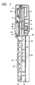
- a portable telephone having an electromagnetic isolation structure according to the first embodiment of the invention.
- the portable telephone includes a printed circuit board 10, a voltage-controlled oscillator (VCO) 11 which changes output frequency by changing tuning voltage, a temperature-compensated crystal oscillator (TCXO) 12 providing frequency stability, an amplifier 13 amplifying the voltage of a high-frequency signal, a modulator 14, a first shield case 15, a second shield case 16, a disc-shaped receiver 17 outputting a voice message from a calling party, a liquid-crystal display 18, a holder 19, an electronic motor 20 for providing vibrations to a telephone casing or body to indicate reception of a call, diaphragm switches 21, a key sheet 22, electronic components 23 such as resistors, diodes, capacitors, and transistors, a cover 24, a bottom casing 25, and a battery 28.
- the battery 28 is attached to a battery mounting flat portion 29 formed on a back surface of the bottom casing 25.
- the printed circuit board 10 has formed on its front surface a first radio communication circuit including the VCO 11 and the TCXO 12 and on its back surface a second radio communication circuit including the amplifier 13 and the modulator 14.
- Each of the first and second shield cases 15 and 16 is formed with a box-like member and made from resin material such as acrylonitrile, butadiene, ABS (styrene), PS (polystyrene), or PC (polycarbonate) and coated with copper in electroless plating.
- the copper plated layer is also coated with nickel in electro or electroless plating for the purpose of rust prevention.
- Each of the first and second shield cases 15 and 16 may alternatively be made from metallic plate such as a nickel silver, an iron, or a copper-plated plate and may also be applied with conductive material or coated with aluminum in vacuum deposition.
- the diaphragm switches 22 are disposed on a portion of the front surface of the printed circuit board 10 below the VCO 11, as viewed in Fig. 1.
- the key sheet 22 on which characters and symbols are printed is disposed on the diaphragm switches 22.
- the electronic components 23 are mounted on a portion of the back surface of the printed circuit board 10 opposite to the diaphragm switches 22.
- the telephone body consists of the cover 24 and the bottom casing 25.
- the cover 24 has formed therein a sound hole 26 through which a voice signal from the receiver 17 is transmitted outside the telephone body and a light-transmitting opening 27 through which the light from the display 18 is transmitted.
- the light-transmitting opening 27 is smaller in diameter than the liquid-crystal display 18.
- the first shield case 15 is, as shown in Figs. 2 and 3, formed with a first upper wall 30, side walls 31 surrounding the first upper wall 30, and edge walls 32 extending, as clearly shown in Fig. 3, from the side walls 31 outside an edge of the printed circuit board 10.
- the first upper wall 30 has formed thereon a plurality of barb-like claws 33 and 34 for retaining the receiver 17 and the holder 19 on which the rectangular display 18 is installed.
- the holder 19 is made from white or transparent resin which establishes multiple reflections of light emitted from a light-emitting diode (not shown) mounted on the printed circuit board 10 to illuminate the back surface of the display 18 for visually indicating numbers, characters, or symbols thereon.
- the side walls 31 surround electronic components such as the VCO 11 and TCXO 12 mounted on the printed circuit board 10.
- the first upper wall 30 has formed on its inner surface a plurality of first rectangular ribs 35 to define enclosed chambers along with the side walls 31 for insulating the VCO 11, the TCXO 12, and other electronic components on the printed circuit board 10 from each other.
- the edge walls 32 have formed thereon at given intervals a plurality of barb-like claws 36 engaging the second shielding case 16. Other portions of the edge walls 32 between the claws 36 may be in contact with or separate at small intervals from the second shielding case 16.
- the second shielding case 16 is, as shown in Fig. 3, formed with a second upper wall 37, first side walls 38 surrounding the second upper wall 37, and L-shaped second side walls 39 extending from edges of the first side walls 38.
- the printed circuit board 10 is mounted on the edges of the first side walls 38 with a grounding conductor(s) printed on the printed circuit board 10 being in contact therewith.
- the second side walls 39 surround the edges of the printed circuit board 10.
- the second upper wall 37 has formed on its inner surface a plurality of rectangular ribs 40 which extend inward on a level with the first side walls 38 to define enclosed chambers along with the first side walls 38 for insulating the amplifier 13, the modulator 14, and other circuit components mounted on the printed circuit board 10 from each other. Edges of the ribs 40 are also in contact with the grounding conductor(s) on the printed circuit board 10.
- the second side walls 39 have formed thereon barb-like claws 41 to establish engagement with the claws formed on the first shielding case 15 above the printed circuit board 10.
- the second upper wall 37 has, as shown in Fig. 3, formed on its outer surface a rectangular frame 42 defining a chamber within which the motor 20 is mounted.
- the motor 20, as described above, provides vibrations to the telephone body to inform a telephone user of reception of a call and has a motor body 45 wrapped in a motor cushion 53 and a weight 44 supported eccentrically on an output shaft 43 thereof.
- the output shaft 43 extends substantially in parallel to the printed circuit board 10.
- the cover 24 has formed on its inner surface an annular rib 46 facing the receiver 17.
- the nonwoven fabric cloth 47 is attached to the annular rib 46.
- a receiver cushion 48 is disposed on an edge of the rib 46 through the nonwoven fabric cloth 47.
- the receiver cushion 48 is formed with an annular elastic member made of chloroprene rubber, polyurethane rubber, natural or synthetic rubber, urethane rubber, or silicone rubber which is proof against sound, dust, and water.
- the annular rib 46 is smaller in outer diameter than the receiver cushion 48, while it is greater in inner diameter than the receiver cushion 48. Specifically, the receiver cushion 48 covers the whole of the edge of the annular rib 46.
- a transparent window 49 is installed in the cover 24 so as to cover the light-transmitting opening 27.
- a hollow rectangular liquid-crystal display cushion 50 is attached to the inner wall of the cover 24 outside the light-transmitting opening 49 in constant engagement with the outer surface of the display 18 and is made of an elastic material such as polyurethane foam, polyethylene foam, polystyrene foam, chloroprene rubber, polyurethane rubber, natural or synthetic rubber, urethane rubber, or silicone rubber.
- the thickness c as shown in Fig. 2, of the liquid-crystal display cushion 50 is greater than a second clearance d that is the interval between the inner surface of the cover 24 and the display 18 (i.e., the upper edge of the holder 19). This results in elastic deformation of the liquid-crystal cushion 50 between the inner surface of the cover 24 and the display 18 (the holder 19) to produce pressure urging the first shield case 15 toward the printed circuit board 10.
- the cover 24 also has a plurality of guide members 52, as shown in Fig. 3, formed on the inner surface thereof at small intervals away from the first shield case 15.
- the guide members 52 serve to position the first and second shield cases 15 and 16 within the telephone body.
- the elastic deformation of the receiver cushion 48, the liquid-crystal cushion 50, and the motor cushion 53 produces elastic pressure acting on the first and second shield cases 15 and 16 inward of the telephone body to establish constant conductive communications between the first and second shield cases 15 and 16 and between the printed circuit board 10 and the first and second shield cases 15 and 16.
- first and second shield cases 15 and 16 are attached to each other through the claws 36 and 41 provided on three of the side walls of each of the first and second shield cases 15 and 16 to surround a portion of the printed circuit board 10, however, may alternatively surround the whole of the printed circuit board 10 by the four side walls of each of the first and second shield cases 15 and 16 to isolate it electromagnetically from the outside of the first and second shield cases 15 and 16.
- the motor body 45 of the motor 20 is wrapped in the motor cushion 53 and then fitted into the frame 42 with the weight 44 projecting from the frame 42.
- This preassembly is then put into the bottom casing 25 with the back surface of the printed circuit board 10 facing the bottom casing 25.
- the disc-shaped receiver 17 is installed by the claws 33.
- the holder 19 in which the liquid-crystal display 18 is mounted is held by the claws 34.
- the cover 24 having attached thereto the nonwoven fabric cloth 47, the receiver cushion 48, and the liquid-crystal display cushion 50 is fitted on the bottom casing 25.
- the height f of the motor cushion 53 is, as shown in Fig. 3, greater than the third clearance e , so that the motor cushion 53 is partly compressed by an amount of (f - e) to produce elastic pressure F3 which urges the second shield case 16 onto the printed circuit board 10.
- the thickness c of the liquid-crystal cushion 50 is greater than the second clearance d , so that the liquid-crystal cushion 50 is partly compressed between the inner wall of the cover 24 and the liquid-crystal display 18 and the holder 19 by an amount of (c - d) to produce elastic pressure F2, as shown in Fig. 2, which urges the first shield case 15 into constant engagement with the printed circuit board 10.
- This also defines an enclosed chamber between the liquid-crystal display 18 and the transparent window 49 which blocks entry of dust from the outside.
- the edge walls 32 of the first shield case 15 may alternatively be separate from the second side walls 39 of the second shield case 16 through a small gap.
- the inventors of this application have experimentally found that when such a small gap is less than or equal to 0.5mm, and a wall is provided between the gap and electronic components in a portable telephone used within a band of 8000MHz, for example, the electronic components are insulated from unwanted electromagnetic waves or noise.
- that wall corresponds to the side wall 31 of the first shield case 15 provided inside the second side wall 39 of the second shield case 16.
- Fig. 4 shows an electrical isolation structure for a portable telephone according to the second embodiment of the invention which is different from the above first embodiment in that a plurality of springs 57 are disposed between the first shield case 15 and the printed circuit board 10 and between the second shield case 16 and the printed circuit board 10.
- a plurality of springs 57 are disposed between the first shield case 15 and the printed circuit board 10 and between the second shield case 16 and the printed circuit board 10.
- Other arrangements are identical, and explanation thereof in detail will be omitted here.
- a plurality of first recessed portions 55 having the same depth are formed at given intervals in ends of the side walls 31 and the first rectangular ribs 35 extending from the first upper wall 30 of the first shield case 15.
- a plurality of second recessed portions 59 are formed at given intervals in ends of the second rectangular ribs 40 extending from the second upper wall 37 of the second shield case 16.
- the springs 57 made of beryllium steel or phosphor bronze are disposed within the first and second recessed portions 55 and 59 one in each in electric contact with the grounding conductor(s) on the printed circuit board 10.
- the springs 57 are slightly compressed between the recessed portions 55 and 59 and the surfaces of the printed circuit board 10 to produce reaction pressures urging the first and second shield cases 15 and 16 into disengagement from the printed circuit board 10.
- Each of the springs 57 may be soldered to the grounding conductor of the printed circuit board 10 or alternatively be bonded at a curved portion 58 to one of the first and second recessed portions 55 and 59.
- the motor body 45 of the motor 20 is wrapped in the motor cushion 53 and then fitted into the frame 42.
- the disc-shaped receiver 17 is fitted to the claws 33.
- the holder 19 in which the liquid-crystal display 18 is mounted is fitted to the claws 34.
- the cover 24 having attached thereto the nonwoven fabric cloth 47, the receiver cushion 48, and the liquid-crystal display cushion 50 is fitted on the bottom casing 25.
- the motor cushion 53 is compressed between the second shield case 16 and the pressure ribs 54 to produce the elastic pressure F3, as discussed above with reference to Fig. 3, which urges the second shield case 16 onto the printed circuit board 10.
- the elastic pressure F3 is set greater than the pressure F5 produced by the springs 57 installed in the second recessed portions 59 of the second shield case 16, which establishes conductive engagement of the first side walls 38 of the second shield case 16 and the flat edge portions 60 of the second rectangular ribs 40 with the printed circuit board 10 and which compresses the springs 57 within the second recessed portions 59 to establish conductive engagement of the second recessed portions 59 with the printed circuit board 10.
- the receiver cushion 48 is, as discussed above, compressed between the cover 24 and the receiver 17 to produce the elastic pressure F1 urging the first shield case 15 toward the printed circuit board 10.
- the liquid-crystal cushion 50 is also compressed between the cover 24 and the holder 19 to produce the elastic pressure F2 urging the first shield case 15 toward the printed circuit board 10.
- the elastic pressures F1 and F2 are so determined as to meet relations of F1 > F5, F2 > F5, and (F1 + F2) > F5. This establishes conductive engagement of the side walls 31 of the first shield case 15 and the flat edge portions 56 of the first rectangular ribs 35 with the printed circuit board 10 and compresses the springs 57 within the first recessed portions 55 to establish conductive engagement of the first recessed portions 55 with the printed circuit board 10.
- the springs 57 of this embodiment serve to establish constant engagement of the first and second shield cases 15 and 16 with the grounding conductor(s) on the printed circuit board 10 even if the first and second shield cases 15 and 16, for example, the first and second ribs 35 and 40 are deformed or curved, which will develop gaps between themselves and the printed circuit board 10.
- Additional springs may be disposed between the first side walls 38 of the second shield case 16 and the printed circuit board 10 to increase the conductive engagement of the second shield case 16 with the printed circuit board 10.
Landscapes
- Engineering & Computer Science (AREA)
- Microelectronics & Electronic Packaging (AREA)
- Signal Processing (AREA)
- Shielding Devices Or Components To Electric Or Magnetic Fields (AREA)
- Telephone Set Structure (AREA)
Applications Claiming Priority (3)
| Application Number | Priority Date | Filing Date | Title |
|---|---|---|---|
| JP25473896 | 1996-09-26 | ||
| JP25473896 | 1996-09-26 | ||
| JP254738/96 | 1996-09-26 |
Publications (3)
| Publication Number | Publication Date |
|---|---|
| EP0833466A2 true EP0833466A2 (de) | 1998-04-01 |
| EP0833466A3 EP0833466A3 (de) | 1998-05-20 |
| EP0833466B1 EP0833466B1 (de) | 2005-03-23 |
Family
ID=17269182
Family Applications (1)
| Application Number | Title | Priority Date | Filing Date |
|---|---|---|---|
| EP97307529A Expired - Lifetime EP0833466B1 (de) | 1996-09-26 | 1997-09-25 | Vorrichtung zur elektromagnetischen Isolierung eines elektronischen Gerätes |
Country Status (5)
| Country | Link |
|---|---|
| US (2) | US6333459B1 (de) |
| EP (1) | EP0833466B1 (de) |
| CN (2) | CN1177519C (de) |
| DE (1) | DE69732823T2 (de) |
| IN (1) | IN192428B (de) |
Cited By (8)
| Publication number | Priority date | Publication date | Assignee | Title |
|---|---|---|---|---|
| WO1999057871A1 (en) * | 1998-04-22 | 1999-11-11 | Increa Oy | Radiophone |
| EP1001585A2 (de) * | 1998-11-10 | 2000-05-17 | Matsushita Electric Industrial Co., Ltd. | Tragbares Endgerät |
| EP1037391A2 (de) * | 1999-03-18 | 2000-09-20 | Matsushita Electric Industrial Co., Ltd. | Funkendgerät |
| EP1096757A2 (de) * | 1999-10-26 | 2001-05-02 | Matsushita Electric Industrial Co., Ltd. | Stecker-Halterung für eine Hörkapsel |
| EP1427268A1 (de) * | 2001-09-14 | 2004-06-09 | Matsushita Electric Industrial Co., Ltd. | Tragbare elektronische vorrichtung und bga-verkapselungs-schutzeinrichtung |
| JP2015045757A (ja) * | 2013-08-28 | 2015-03-12 | 株式会社ニコン | 電子機器 |
| EP3288351A1 (de) * | 2016-08-22 | 2018-02-28 | Woodward, Inc. | Rahmen für leiterplattenträger bei hohen schwingungen |
| JP2018142009A (ja) * | 2018-05-02 | 2018-09-13 | 株式会社ニコン | 電子機器 |
Families Citing this family (33)
| Publication number | Priority date | Publication date | Assignee | Title |
|---|---|---|---|---|
| IN192428B (de) * | 1996-09-26 | 2004-04-24 | Matsushita Electric Ind Co Ltd | |
| FI115108B (fi) * | 1997-10-06 | 2005-02-28 | Nokia Corp | Menetelmä ja järjestely kuulokkeen vuotosiedon parantamiseksi radiolaitteessa |
| FI104282B (fi) * | 1998-05-22 | 1999-12-15 | Jari Ruuttu | Tärinävaimennettu valaisin ja menetelmä tärinävaimennetun valaisimen valmistamiseksi |
| JP2001007550A (ja) * | 1999-06-24 | 2001-01-12 | Nec Corp | 携帯情報無線端末装置およびその製造方法 |
| JP3960115B2 (ja) * | 2001-05-24 | 2007-08-15 | 松下電器産業株式会社 | 携帯用電力増幅器 |
| EP1372243A1 (de) * | 2002-06-11 | 2003-12-17 | Sony Ericsson Mobile Communications AB | Elektronische Vorrichtung mit Rütteleinrichtung und auswechselbarem Deckel |
| AU2003240248A1 (en) | 2002-06-11 | 2003-12-22 | Sony Ericsson Mobile Communications Ab | An electronic device with a vibrator and an exchangeable cover |
| JP3838204B2 (ja) * | 2003-02-19 | 2006-10-25 | 株式会社豊田自動織機 | 電動コンプレッサ及び電動コンプレッサの組立方法 |
| US7814127B2 (en) * | 2003-11-20 | 2010-10-12 | International Business Machines Corporation | Natural language support for database applications |
| JP4112484B2 (ja) * | 2003-12-17 | 2008-07-02 | 株式会社東芝 | 無線機器及び半導体装置 |
| KR101213933B1 (ko) * | 2004-05-31 | 2013-01-09 | 엘지디스플레이 주식회사 | 액정표시장치의 모듈 |
| KR100631193B1 (ko) * | 2004-10-27 | 2006-10-04 | 삼성전자주식회사 | 디스플레이장치 및 그것을 구비하는 휴대폰 |
| JP4511408B2 (ja) * | 2005-04-18 | 2010-07-28 | 富士通株式会社 | 表示モジュールおよび携帯端末装置 |
| US20060259918A1 (en) * | 2005-05-16 | 2006-11-16 | Dell Products L.P. | Method and apparatus for mounting a storage device in an information handling system |
| US7636245B2 (en) * | 2007-06-25 | 2009-12-22 | Novatel Wireless, Inc. | Electronic component cover and arrangement |
| CN101360390B (zh) * | 2007-08-03 | 2011-05-04 | 深圳富泰宏精密工业有限公司 | 印刷电路板堆叠结构 |
| US7768465B2 (en) * | 2007-09-12 | 2010-08-03 | Laird Technologies, Inc. | Vehicle-mount stacked patch antenna assemblies with resiliently compressible bumpers for mechanical compression to aid in electrical grounding of shield and chassis |
| CN101453850B (zh) * | 2007-12-06 | 2011-06-22 | 英业达股份有限公司 | 隔振搭接装置 |
| JP2009239261A (ja) * | 2008-03-07 | 2009-10-15 | Panasonic Corp | 電子ユニット、電子装置 |
| US20090290319A1 (en) * | 2008-05-20 | 2009-11-26 | Apple Inc. | Electromagnetic shielding in small-form-factor device |
| US8059418B2 (en) * | 2009-04-03 | 2011-11-15 | Trw Automotive U.S. Llc | Assembly with a printed circuit board |
| CN102577656B (zh) * | 2010-04-20 | 2016-01-20 | 怡得乐精密机械(新加坡)有限公司 | 电磁干扰屏蔽配置 |
| CN102452008A (zh) * | 2010-10-21 | 2012-05-16 | 张家港市贝尔机械有限公司 | 一种快速拆卸螺母 |
| CN103227537B (zh) * | 2013-04-24 | 2016-04-20 | 捷和电机制品(深圳)有限公司 | 印刷电路板及直流电机 |
| KR20140142600A (ko) * | 2013-06-04 | 2014-12-12 | 삼성전자주식회사 | 전자 기기의 보호 장치 및 그를 구비하는 전자 기기 |
| KR102208686B1 (ko) * | 2014-08-11 | 2021-01-28 | 삼성전자주식회사 | 전자 장치 및 그 제작 방법 |
| CN205124242U (zh) * | 2015-10-16 | 2016-03-30 | 中兴通讯股份有限公司 | 一种电子设备 |
| CN106824016B (zh) * | 2017-02-28 | 2019-04-09 | 二重(德阳)重型装备有限公司 | 沸腾床渣油加氢反应器分配盘立式安装方法 |
| KR101919454B1 (ko) * | 2017-07-31 | 2018-11-16 | 엘지디스플레이 주식회사 | 디스플레이 장치 및 이를 이용한 컴퓨팅 장치 |
| CN111083899B (zh) * | 2019-12-19 | 2021-08-06 | 远峰科技股份有限公司 | 车载娱乐主机箱及车载娱乐主机 |
| US11751362B2 (en) | 2021-10-22 | 2023-09-05 | International Business Machines Corporation | Thermally activated retractable EMC protection |
| US11871550B2 (en) | 2021-10-22 | 2024-01-09 | International Business Machines Corporation | Motor controlled retractable EMC protection |
| US11695240B2 (en) | 2021-10-22 | 2023-07-04 | International Business Machines Corporation | Retractable EMC protection |
Citations (5)
| Publication number | Priority date | Publication date | Assignee | Title |
|---|---|---|---|---|
| DE3515772A1 (de) * | 1985-05-02 | 1986-11-06 | Robert Bosch Gmbh, 7000 Stuttgart | Aus zwei gehaeusehalbschalen bestehendes gehaeuse |
| US4890199A (en) * | 1988-11-04 | 1989-12-26 | Motorola, Inc. | Miniature shield with opposing cantilever spring fingers |
| JPH04215500A (ja) * | 1990-12-14 | 1992-08-06 | Fujitsu Ltd | 無線装置端末のシールド構造 |
| JPH0870195A (ja) * | 1994-08-29 | 1996-03-12 | Japan Radio Co Ltd | プリント回路基板のシールド方法 |
| JPH08222881A (ja) * | 1995-02-10 | 1996-08-30 | Hitachi Denshi Ltd | プリント基板の実装方法 |
Family Cites Families (10)
| Publication number | Priority date | Publication date | Assignee | Title |
|---|---|---|---|---|
| JPS62160599A (ja) | 1986-01-08 | 1987-07-16 | Sanyo Electric Co Ltd | Icカ−ド読み取り書き込み装置 |
| JP2825670B2 (ja) * | 1990-12-14 | 1998-11-18 | 富士通株式会社 | 高周波回路装置のシールド構造 |
| JPH0745982A (ja) * | 1993-07-28 | 1995-02-14 | Toshiba Corp | シールドケースとプリント配線板との接続構造 |
| JPH07250138A (ja) * | 1994-03-09 | 1995-09-26 | Fujitsu Ltd | 携帯無線端末装置 |
| JPH08223260A (ja) * | 1995-02-16 | 1996-08-30 | Fujitsu Ltd | 携帯無線端末装置 |
| US5596487A (en) * | 1995-07-31 | 1997-01-21 | Motorola, Inc. | Apparatus for RF shielding radio circuitry |
| US5642413A (en) * | 1995-08-07 | 1997-06-24 | Little; Randall P. | Telephone call alert device with selectable alert modes |
| JP3664792B2 (ja) * | 1996-01-26 | 2005-06-29 | 富士通株式会社 | 携帯無線機 |
| IN192428B (de) * | 1996-09-26 | 2004-04-24 | Matsushita Electric Ind Co Ltd | |
| US5717577A (en) * | 1996-10-30 | 1998-02-10 | Ericsson, Inc. | Gasketed shield can for shielding emissions of electromagnetic energy |
-
1997
- 1997-09-23 IN IN1769CA1997 patent/IN192428B/en unknown
- 1997-09-25 CN CNB021051585A patent/CN1177519C/zh not_active Expired - Fee Related
- 1997-09-25 CN CN97119382.7A patent/CN1104835C/zh not_active Expired - Fee Related
- 1997-09-25 EP EP97307529A patent/EP0833466B1/de not_active Expired - Lifetime
- 1997-09-25 DE DE69732823T patent/DE69732823T2/de not_active Expired - Lifetime
- 1997-09-26 US US08/938,704 patent/US6333459B1/en not_active Expired - Fee Related
-
2001
- 2001-11-08 US US09/986,440 patent/US6501019B2/en not_active Expired - Fee Related
Patent Citations (5)
| Publication number | Priority date | Publication date | Assignee | Title |
|---|---|---|---|---|
| DE3515772A1 (de) * | 1985-05-02 | 1986-11-06 | Robert Bosch Gmbh, 7000 Stuttgart | Aus zwei gehaeusehalbschalen bestehendes gehaeuse |
| US4890199A (en) * | 1988-11-04 | 1989-12-26 | Motorola, Inc. | Miniature shield with opposing cantilever spring fingers |
| JPH04215500A (ja) * | 1990-12-14 | 1992-08-06 | Fujitsu Ltd | 無線装置端末のシールド構造 |
| JPH0870195A (ja) * | 1994-08-29 | 1996-03-12 | Japan Radio Co Ltd | プリント回路基板のシールド方法 |
| JPH08222881A (ja) * | 1995-02-10 | 1996-08-30 | Hitachi Denshi Ltd | プリント基板の実装方法 |
Non-Patent Citations (3)
| Title |
|---|
| PATENT ABSTRACTS OF JAPAN vol. 016, no. 564 (E-1295), 4 December 1992 & JP 04 215500 A (FUJITSU LTD), 6 August 1992, * |
| PATENT ABSTRACTS OF JAPAN vol. 096, no. 007, 31 July 1996 & JP 08 070195 A (JAPAN RADIO CO LTD), 12 March 1996, * |
| PATENT ABSTRACTS OF JAPAN vol. 096, no. 012, 26 December 1996 & JP 08 222881 A (HITACHI DENSHI LTD), 30 August 1996, * |
Cited By (15)
| Publication number | Priority date | Publication date | Assignee | Title |
|---|---|---|---|---|
| WO1999057871A1 (en) * | 1998-04-22 | 1999-11-11 | Increa Oy | Radiophone |
| EP1001585A2 (de) * | 1998-11-10 | 2000-05-17 | Matsushita Electric Industrial Co., Ltd. | Tragbares Endgerät |
| EP1001585A3 (de) * | 1998-11-10 | 2004-03-24 | Matsushita Electric Industrial Co., Ltd. | Tragbares Endgerät |
| EP1037391A2 (de) * | 1999-03-18 | 2000-09-20 | Matsushita Electric Industrial Co., Ltd. | Funkendgerät |
| US7937127B1 (en) | 1999-03-18 | 2011-05-03 | Panasonic Corporation | Radio terminal device |
| EP1037391A3 (de) * | 1999-03-18 | 2003-08-27 | Matsushita Electric Industrial Co., Ltd. | Funkendgerät |
| EP1096757B1 (de) * | 1999-10-26 | 2008-12-31 | Panasonic Corporation | Stecker-Halterung für eine Hörkapsel |
| EP1096757A2 (de) * | 1999-10-26 | 2001-05-02 | Matsushita Electric Industrial Co., Ltd. | Stecker-Halterung für eine Hörkapsel |
| EP1427268A4 (de) * | 2001-09-14 | 2008-07-02 | Matsushita Electric Ind Co Ltd | Tragbare elektronische vorrichtung und bga-verkapselungs-schutzeinrichtung |
| US7436676B2 (en) | 2001-09-14 | 2008-10-14 | Matsushita Electric Industrial Co., Ltd. | Portable electronic apparatus and BGA package protective device |
| EP1427268A1 (de) * | 2001-09-14 | 2004-06-09 | Matsushita Electric Industrial Co., Ltd. | Tragbare elektronische vorrichtung und bga-verkapselungs-schutzeinrichtung |
| JP2015045757A (ja) * | 2013-08-28 | 2015-03-12 | 株式会社ニコン | 電子機器 |
| EP3288351A1 (de) * | 2016-08-22 | 2018-02-28 | Woodward, Inc. | Rahmen für leiterplattenträger bei hohen schwingungen |
| US10561039B2 (en) | 2016-08-22 | 2020-02-11 | Woodward, Inc. | Frame for printed circuit board support in high vibration |
| JP2018142009A (ja) * | 2018-05-02 | 2018-09-13 | 株式会社ニコン | 電子機器 |
Also Published As
| Publication number | Publication date |
|---|---|
| DE69732823D1 (de) | 2005-04-28 |
| US20020027009A1 (en) | 2002-03-07 |
| CN1177904A (zh) | 1998-04-01 |
| IN192428B (de) | 2004-04-24 |
| EP0833466B1 (de) | 2005-03-23 |
| EP0833466A3 (de) | 1998-05-20 |
| US6333459B1 (en) | 2001-12-25 |
| DE69732823T2 (de) | 2006-05-18 |
| CN1378419A (zh) | 2002-11-06 |
| CN1104835C (zh) | 2003-04-02 |
| US6501019B2 (en) | 2002-12-31 |
| CN1177519C (zh) | 2004-11-24 |
Similar Documents
| Publication | Publication Date | Title |
|---|---|---|
| EP0833466B1 (de) | Vorrichtung zur elektromagnetischen Isolierung eines elektronischen Gerätes | |
| JP2825670B2 (ja) | 高周波回路装置のシールド構造 | |
| EP0976311B1 (de) | Schirmgehäuse und dessen herstellungsverfahren | |
| US4424419A (en) | Electret microphone shield | |
| US6304458B1 (en) | RF shielded LCD assembly and PCB assembly including the same | |
| CN112769988B (zh) | 电子设备 | |
| KR20020059913A (ko) | 휴대용 무선단말기의 접지장치 | |
| EP0077615B1 (de) | Abschirmung für ein Elektret-Mikrophon | |
| US6553119B1 (en) | Acoustic component mounting structure for portable radio unit | |
| US7369673B2 (en) | Speaker supporting device and electronic device comprising this speaker supporting device | |
| CN1140969A (zh) | 减小振动的无线电设备扬声器组件 | |
| JP3292453B2 (ja) | 電子機器のシールド構造 | |
| KR20100020579A (ko) | 휴대 단말기의 쉴드캔 | |
| JPH0629684A (ja) | シールド筐体 | |
| JPH1022671A (ja) | 回路基板用シールド機構 | |
| US7206422B2 (en) | Transducer assembly apparatus | |
| KR100565279B1 (ko) | 전자파 차폐장치 일체형 내장 안테나 및 그 내장안테나를 가지는 휴대용 단말기 | |
| JP2002324996A (ja) | 電子機器のシールド構造 | |
| US6061459A (en) | Surface-mounted electromagnetic sound generating body | |
| JP2001187968A (ja) | 電気電子機器用のガスケット | |
| KR100674184B1 (ko) | 도전성 개스킷의 구조 | |
| US20040263359A1 (en) | Transducer assembly | |
| CN213847459U (zh) | 具有麦克风设备的终端 | |
| JPH09162583A (ja) | シールド構造 | |
| US20070041596A1 (en) | Condenser microphone |
Legal Events
| Date | Code | Title | Description |
|---|---|---|---|
| PUAI | Public reference made under article 153(3) epc to a published international application that has entered the european phase |
Free format text: ORIGINAL CODE: 0009012 |
|
| 17P | Request for examination filed |
Effective date: 19971006 |
|
| AK | Designated contracting states |
Kind code of ref document: A2 Designated state(s): DE FR GB |
|
| PUAL | Search report despatched |
Free format text: ORIGINAL CODE: 0009013 |
|
| AK | Designated contracting states |
Kind code of ref document: A3 Designated state(s): AT BE CH DE DK ES FI FR GB GR IE IT LI LU MC NL PT SE |
|
| AKX | Designation fees paid |
Free format text: DE FR GB |
|
| RBV | Designated contracting states (corrected) |
Designated state(s): DE FR GB |
|
| 17Q | First examination report despatched |
Effective date: 20031103 |
|
| RTI1 | Title (correction) |
Free format text: ELECTROMAGNETIC ISOLATION APPARATUS FOR ELECTRONIC EQUIPMENT |
|
| GRAP | Despatch of communication of intention to grant a patent |
Free format text: ORIGINAL CODE: EPIDOSNIGR1 |
|
| GRAS | Grant fee paid |
Free format text: ORIGINAL CODE: EPIDOSNIGR3 |
|
| GRAA | (expected) grant |
Free format text: ORIGINAL CODE: 0009210 |
|
| AK | Designated contracting states |
Kind code of ref document: B1 Designated state(s): DE FR GB |
|
| REG | Reference to a national code |
Ref country code: GB Ref legal event code: FG4D |
|
| REF | Corresponds to: |
Ref document number: 69732823 Country of ref document: DE Date of ref document: 20050428 Kind code of ref document: P |
|
| PLBE | No opposition filed within time limit |
Free format text: ORIGINAL CODE: 0009261 |
|
| STAA | Information on the status of an ep patent application or granted ep patent |
Free format text: STATUS: NO OPPOSITION FILED WITHIN TIME LIMIT |
|
| ET | Fr: translation filed | ||
| 26N | No opposition filed |
Effective date: 20051227 |
|
| PGFP | Annual fee paid to national office [announced via postgrant information from national office to epo] |
Ref country code: DE Payment date: 20100922 Year of fee payment: 14 |
|
| PGFP | Annual fee paid to national office [announced via postgrant information from national office to epo] |
Ref country code: FR Payment date: 20110922 Year of fee payment: 15 Ref country code: GB Payment date: 20110921 Year of fee payment: 15 |
|
| GBPC | Gb: european patent ceased through non-payment of renewal fee |
Effective date: 20120925 |
|
| REG | Reference to a national code |
Ref country code: FR Ref legal event code: ST Effective date: 20130531 |
|
| PG25 | Lapsed in a contracting state [announced via postgrant information from national office to epo] |
Ref country code: DE Free format text: LAPSE BECAUSE OF NON-PAYMENT OF DUE FEES Effective date: 20130403 Ref country code: GB Free format text: LAPSE BECAUSE OF NON-PAYMENT OF DUE FEES Effective date: 20120925 |
|
| PG25 | Lapsed in a contracting state [announced via postgrant information from national office to epo] |
Ref country code: FR Free format text: LAPSE BECAUSE OF NON-PAYMENT OF DUE FEES Effective date: 20121001 |
|
| REG | Reference to a national code |
Ref country code: DE Ref legal event code: R119 Ref document number: 69732823 Country of ref document: DE Effective date: 20130403 |