EP0809129B1 - Optischer Halbleitermodulator und sein Herstellunsgverfahren - Google Patents
Optischer Halbleitermodulator und sein Herstellunsgverfahren Download PDFInfo
- Publication number
- EP0809129B1 EP0809129B1 EP97108311A EP97108311A EP0809129B1 EP 0809129 B1 EP0809129 B1 EP 0809129B1 EP 97108311 A EP97108311 A EP 97108311A EP 97108311 A EP97108311 A EP 97108311A EP 0809129 B1 EP0809129 B1 EP 0809129B1
- Authority
- EP
- European Patent Office
- Prior art keywords
- semiconductor
- absorption layer
- semiconductor optical
- optical absorption
- layer
- Prior art date
- Legal status (The legal status is an assumption and is not a legal conclusion. Google has not performed a legal analysis and makes no representation as to the accuracy of the status listed.)
- Expired - Lifetime
Links
Images


Classifications
-
- G—PHYSICS
- G02—OPTICS
- G02F—OPTICAL DEVICES OR ARRANGEMENTS FOR THE CONTROL OF LIGHT BY MODIFICATION OF THE OPTICAL PROPERTIES OF THE MEDIA OF THE ELEMENTS INVOLVED THEREIN; NON-LINEAR OPTICS; FREQUENCY-CHANGING OF LIGHT; OPTICAL LOGIC ELEMENTS; OPTICAL ANALOGUE/DIGITAL CONVERTERS
- G02F1/00—Devices or arrangements for the control of the intensity, colour, phase, polarisation or direction of light arriving from an independent light source, e.g. switching, gating or modulating; Non-linear optics
- G02F1/01—Devices or arrangements for the control of the intensity, colour, phase, polarisation or direction of light arriving from an independent light source, e.g. switching, gating or modulating; Non-linear optics for the control of the intensity, phase, polarisation or colour
- G02F1/015—Devices or arrangements for the control of the intensity, colour, phase, polarisation or direction of light arriving from an independent light source, e.g. switching, gating or modulating; Non-linear optics for the control of the intensity, phase, polarisation or colour based on semiconductor elements having potential barriers, e.g. having a PN or PIN junction
- G02F1/025—Devices or arrangements for the control of the intensity, colour, phase, polarisation or direction of light arriving from an independent light source, e.g. switching, gating or modulating; Non-linear optics for the control of the intensity, phase, polarisation or colour based on semiconductor elements having potential barriers, e.g. having a PN or PIN junction in an optical waveguide structure
-
- G—PHYSICS
- G02—OPTICS
- G02F—OPTICAL DEVICES OR ARRANGEMENTS FOR THE CONTROL OF LIGHT BY MODIFICATION OF THE OPTICAL PROPERTIES OF THE MEDIA OF THE ELEMENTS INVOLVED THEREIN; NON-LINEAR OPTICS; FREQUENCY-CHANGING OF LIGHT; OPTICAL LOGIC ELEMENTS; OPTICAL ANALOGUE/DIGITAL CONVERTERS
- G02F1/00—Devices or arrangements for the control of the intensity, colour, phase, polarisation or direction of light arriving from an independent light source, e.g. switching, gating or modulating; Non-linear optics
- G02F1/01—Devices or arrangements for the control of the intensity, colour, phase, polarisation or direction of light arriving from an independent light source, e.g. switching, gating or modulating; Non-linear optics for the control of the intensity, phase, polarisation or colour
- G02F1/015—Devices or arrangements for the control of the intensity, colour, phase, polarisation or direction of light arriving from an independent light source, e.g. switching, gating or modulating; Non-linear optics for the control of the intensity, phase, polarisation or colour based on semiconductor elements having potential barriers, e.g. having a PN or PIN junction
- G02F1/0155—Devices or arrangements for the control of the intensity, colour, phase, polarisation or direction of light arriving from an independent light source, e.g. switching, gating or modulating; Non-linear optics for the control of the intensity, phase, polarisation or colour based on semiconductor elements having potential barriers, e.g. having a PN or PIN junction modulating the optical absorption
- G02F1/0157—Devices or arrangements for the control of the intensity, colour, phase, polarisation or direction of light arriving from an independent light source, e.g. switching, gating or modulating; Non-linear optics for the control of the intensity, phase, polarisation or colour based on semiconductor elements having potential barriers, e.g. having a PN or PIN junction modulating the optical absorption using electro-absorption effects, e.g. Franz-Keldysh [FK] effect or quantum confined stark effect [QCSE]
-
- G—PHYSICS
- G02—OPTICS
- G02F—OPTICAL DEVICES OR ARRANGEMENTS FOR THE CONTROL OF LIGHT BY MODIFICATION OF THE OPTICAL PROPERTIES OF THE MEDIA OF THE ELEMENTS INVOLVED THEREIN; NON-LINEAR OPTICS; FREQUENCY-CHANGING OF LIGHT; OPTICAL LOGIC ELEMENTS; OPTICAL ANALOGUE/DIGITAL CONVERTERS
- G02F2203/00—Function characteristic
- G02F2203/25—Frequency chirping of an optical modulator; Arrangements or methods for the pre-set or tuning thereof
- G02F2203/255—Negative chirp
Definitions
- This invention relates to a semiconductor optical modulator, and more particularly to, an electroabsorption-type optical modulator in which the absorption of a light wave supplied is controlled by changing an intensity of electric field applied to a semiconductor optical absorption layer, and relates to a method for making the same.
- the external optical modulators can be composed of dielectric materials such as LiNbO3 or semiconductor materials such as InP, GaAs.
- semiconductor optical modulators are attractive since they can be integrated with optical elements such as a semiconductor laser, an optical amplifier or electronic circuits such as FET and can be easily miniaturized and operated with a reduced voltage.
- the semiconductor optical modulators include absorption-type optical modulators in which the intensity modulation is conducted by varying an optical absorption coefficient based on an effect that the absorption edge is shifted to a long-wave end by applying an electric field, e.g., a Franz-Keldish effect in bulk semiconductor or a quantum cofined Stark effect in multiquantum well(MQW), and Mach-Zehnder-type modulators which utilize a refractive index variation caused by an electrooptic effect(Pockels effect) or the quantum confined effect in bulk semiconductor.
- absorption-type optical modulators in which the intensity modulation is conducted by varying an optical absorption coefficient based on an effect that the absorption edge is shifted to a long-wave end by applying an electric field, e.g., a Franz-Keldish effect in bulk semiconductor or a quantum cofined Stark effect in multiquantum well(MQW)
- MQW multiquantum well
- the chirping can be reduced to zero.
- a simple linear waveguide structure as in the absorption-type modulators cannot be obtained, therefore its fabrication and operation are complicated.
- the wavelength chirping is much lower than that of the semiconductor laser direct modulation manner, but it cannot be reduced to zero.
- electroabsorption-type optical modulators when an electric field corresponding to an electrical signal is applied to an optical absorption layer, the absorption coefficient for an incident light with a wavelength ( ⁇ op ) longer than the absorption-edge wavelength of the optical absorption layer of the modulator is increased to extinguish the incident light.
- FIG.1 shows detuning ⁇ (a difference between the wavelength of an incident light and the absorption-edge wavelength of the optical absorption layer) and applied electric field dependencies of the absorption coefficient.
- the chirping can be reduced by superposing a signal electric field corresponding to an electrical signal after applying a constant electric field to an electroabsorption-type optical modulator.
- an electroabsorption-type optical modulator has been expected to be a modulator for ultra-high speed and long distance optical communications in the future.
- the pre-bias applying techniques where a constant bias is previously applied to the electroabsorption-type optical modulator have merits that the chirping can be reduced and the limitation to the transmission distance due to the dispersion can be overcome.
- the emission power in the ON state of light is decreased and the extinction ratio is deteriorated when the pre-bias is applied.
- a drive circuit(bias T circuit) for applying a constant bias to an external electrical signal as shown in FIG.3 is required.
- GB-PS 2 243 456 shows an electroabsorption optical modulator according to the preamble part of claim 1.
- an object of the invention to provide an electroabsorption-type optical modulator in which a negative chirp during a modulation can be obtained without previously applying a constant bias and a sufficient light emission power and a good distinction ratio can be obtained.
- An electroabsorption-type optical modulator comprises:
- An electroabsorption-type optical modulator comprises:
- An electroabsorption-type optical modulator comprises:
- a method for making a semiconductor optical modulator comprises the steps of:
- an optical communication module comprises:
- an optical communication system comprises:
- the semiconductor electroabsorption-type optical modulator has an optical absorption layer with a plurality of regions with different absorption-edge wavelengths along the direction of waveguiding a light, i.e., the optical absorption layer includes a region where a absorption-edge wavelength is shifted to a long-wave side rather than usual. Therefore, when a uniform electric field is applied to the regions, as the entire modulator, the refractive index is varied to a negative direction and the absorption coefficient is increased. Also, the ratio of lengths of the short-wave side and the long-wave side of the absorption layer is properly determined so that the absorption coefficient of the entire absorption layer is sufficiently small when no bias is applied. Thus, a negative chirp during a modulation can be obtained without previously applying a constant bias and a sufficient light emission power and a good extinction ratio can be obtained.
- this invention employs a bandgap control technique using a selective MOVPE(metal organic vapor phase epitaxy) method.
- a selective MOVPE(metal organic vapor phase epitaxy) method According as each of the widths of dielectric mask regions on both sides of the blank region is partially varied, the absorption-edge wavelength of the optical absorption layer is partially varied.
- the crystal growth method the optical absorption layer with partially different absorption-edge wavelengths can be formed in one growth step, i.e., it is not necessary to repeat an etching and a crystal growth for divided regions. Therefore, an electroabsorption-type optical modulator can be made with a good uniformity, reproducibility and controllability.
- FIGS.5A to 5H show a method for making the InP-system multiquantum well(MQW) electroabsorption-type optical modulator, wherein FIGS.5A to 5H are cross sectional views cut along the line A-A' in FIG.4.
- a n-InP buffer layer 102 with a thickness of 0.8 ⁇ m and a carrier concentration of 1x10 17 cm -3 is formed on the entire surface of a (100) direction n-InP substance 101(FIG.5A).
- a SiO 2 film with a thickness of 1000 ⁇ to provide a dielectric mask for selective growth is grown thereon, patterning the SiO 2 film by using a standard photolithography technique, thereby forming a first SiO 2 mask 201 for selective growth(FIG.5B).
- FIG.6 shows the pattern of the first SiO 2 mask 201 for selective growth which is seen from a position over the wafer.
- an absorption layer of the electroabsorption-type optical modulator is formed in a blank region 302 which is sandwiched between two regions of the SiO 2 mask 201.
- the absorption layer for a long-wave side absorption-edge wavelength corresponding to the narrow-width area of the SiO 2 mask 201 and the absorption layer for a short-wave side absorption-edge wavelength corresponding to the broad-width area of the SiO 2 mask 201 are formed.
- a n-InP cladding layer 202 with a thickness of 700 ⁇ and a carrier concentration of 1x10 17 cm -3 a MQW optical absorption layer 203(eighteen periods of InGaAsP(6nm)/InGaAsP(5.8nm)) with a thickness of 2124 ⁇ and a carrier concentration of 5x10 15 cm -3 and a p-InP cladding layer 204 with a thickness of 1600 ⁇ and a carrier concentration of 5x10 17 cm -3 are formed in this order(FIG.5C).
- FIG.7 shows the pattern of the second SiO 2 mask 205 for selective growth which is seen from a position over the wafer.
- a blank region 209 between the second SiO 2 masks 205 for selective growth has a width broader than that of the first SiO 2 mask 201 for selective growth.
- a p-buried cladding layer 207 with a thickness of 1.6 ⁇ m and a carrier concentration of 5x10 17 cm -3 , a p-InGaAs capping layer 208 with a thickness of 0.25 ⁇ m and a carrier concentration of 1x10 19 cm -3 are formed(FIG.5E).
- a polyimide film 301 with a thickness of 3 ⁇ m is formed thereon(FIG.5F).
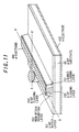
- FIG.10 is a cross sectional view of the fabricated device cut along the line B-B' in FIG.4.
- the absorption-edge wavelength ⁇ g1 in region 1 is set to be longer than the absorption-edge wavelength ⁇ g2 in region 2.
- a light wave with a wavelength of 1.55 ⁇ m supplied to the InP-system MQW electroabsorption-type optical modulator shown in FIG.4 is emitted substantially without being absorbed when an external bias of 0V is applied to the modulator(light ON state), and it is absorbed to extinguish the light when an external bias of 2V is applied(light OFF state).
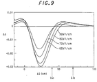
- variations of the absorption coefficient and the refractive index in the long-wave and short-wave sides of the optical absorption layer of the electroabsorption-type -type optical modulator are shown in FIGS.8 and 9.
- the waveguide length of the short-wave side optical absorption layer L 1 is 30 ⁇ m and the waveguide length of the long-wave side optical absorption layer L 2 is 150 ⁇ m.
- the electroabsorption-type optical modulator has a characteristic of ⁇ 0.
- the negative chirping modulation operation can be performed without previously applying a DC bias and without causing an increase in absorption loss.
- the electroabsorption-type optical modulator shown in FIG.4 since the polyimide film 301 is thick buried under the pad, the pad capacity can be reduced.
- the electroabsorption-type optical modulator in the first embodiment can be used for such a high-speed modulation as 10 Gb/s.
- the invention is not limited to the above embodiment, where the InP-system MQW structure electroabsorption-type optical modulator is used, and may employ a InGaAs/InP MQW or a Al-system MQW. Also, the invention is not limited to the device form, for example, the thicknesses and compositions of the respective layers(films) or the dimension of the waveguide, in the first embodiment.
- FIGS.12A to 12H show a method for making the InP-system multiquantum well(MQW) electroabsorption-type optical modulator, wherein FIGS.12A to 12H are cross sectional views cut along the line A-A' in FIG.11.
- a n-InP buffer layer 102 with a thickness of 0.8 ⁇ m and a carrier concentration of 1x10 17 cm -3 is formed on the entire surface of a (100) direction n-InP substance 101(FIG.12A).
- a SiO 2 film with a thickness of 1000 ⁇ to provide a dielectric mask for selective growth is grown thereon, patterning the SiO 2 film by using a standard photolithography technique, thereby forming a first SiO 2 mask 501 for selective growth(FIG.12B).
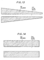
- FIG.13 shows the pattern of the first SiO 2 mask 501 for selective growth which is seen from a position over the wafer.
- an absorption layer of the electroabsorpticn-type optical modulator is formed in a blank region 502 which is sandwiched between two regions of the SiO 2 mask 501.
- the absorption layer for a long-wave side absorption-edge wavelength corresponding to the narrow-width area of the SiO 2 mask 501 and the absorption layer for a short-wave side absorption-edge wavelength corresponding to the broad-width area of the SiO 2 mask 501 are formed.
- a n-InP cladding layer 202 with a thickness of 700 ⁇ and a carrier concentration of 1x10 17 cm -3 a MQW optical absorption layer 203(eighteen periods of InGaAsP(6nm)/InGaAsP(5.8nm)) with a thickness of 2124 ⁇ and a carrier concentration of 5x10 15 cm -3 and a p-InP cladding layer 204 with a thickness of 1600 ⁇ and a carrier concentration of 5x10 17 cm -3 are formed in this order(FIG.12C).
- FIG.14 shows the pattern of the second SiO 2 mask 505 for selective growth which is seen from a position over the wafer.
- a blank region 509 between the second SiO 2 masks 505 for selective growth has a width broader than that of the first SiO 2 mask 501 for selective growth.
- a p-buried cladding layer 207 with a thickness of 1.6 ⁇ m and a carrier concentration of 5x10 17 cm -3 , a p-InGaAs capping layer 208 with a thickness of 0.25 ⁇ m and a carrier concentration of 1x10 19 cm -3 are formed(FIG.12E).
- a polyimide film 301 with a thickness of 3 ⁇ m is formed thereon(FIG.12F).
- FIG.15 is a cross sectional view of the fabricated device cut along the line B-B' in FIG.11.
- the absorption-edge wavelength ⁇ g is set to be gradually changed from the long-wave side to the short-wave side along the direction of waveguiding light. Therefore, a sudden change of the absorption-edge wavelength in the optical absorption layer can be relaxed and reflection of a light wave or a radiation loss due to mode mismatching inside the optical absorption layer can be reduced as well as performing a negative chirping operation without applying a pre-bias.
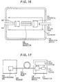
- the modulator module 618 for optical communications comprises the semiconductor electroabsorption-type optical modulator 619 in the first or second embodiment on a sub-mount 617, spherical lenses 612, 612 and optical fibers 613, 613.
- the module 619 By using the module 619, a high-speed transmission of optical signal with a low insertion loss and a low chirp can be performed.
- a transmitter includes a light source 621 for inputting a light to the modulator module 618 for optical communications and a drive system 622 for driving the modulator module 618 and the light source 621.
- the light from the light source 621 is converted into an optical signal by the modulator module 618 for optical communications, transmitted through an optical fiber 623, and detected by a light-receiving unit 625 of a receiver 624.
- the electroabsorption-type optical modulator in which the negative chirping modulation can be performed without applying a constant bias and without increasing an absorption loss in the ON state of light, can be obtained without requiring the complicated fabrication process and with a good yield.
- the optical absorption waveguide of the electroabsorption-type optical modulator when the optical absorption waveguide of the electroabsorption-type optical modulator is fabricated, it can be formed by patterning the thin dielectric film such as SiO 2 to provide a mask for the selective growth and conducting the selective crystal growth, without using any etching process of semiconductor.
- the region needs only to be sandwiched with the SiO 2 mask.
- the thin dielectric film over the broad area with a good reproducibility is much easier than to etch a semiconductor up to an order of ⁇ m.
Landscapes
- Physics & Mathematics (AREA)
- Nonlinear Science (AREA)
- General Physics & Mathematics (AREA)
- Optics & Photonics (AREA)
- Optical Modulation, Optical Deflection, Nonlinear Optics, Optical Demodulation, Optical Logic Elements (AREA)
- Optical Integrated Circuits (AREA)
- Optical Communication System (AREA)
- Semiconductor Lasers (AREA)
Claims (9)
- Optischer Modulator der Elektroabsorptionsbauart, mit:wobei die Absorption einer Lichtwelle, die einem Ende der optischen Absorptions-Halbleiterschicht (203) zugeführt wird, durch Ändern der Intensität eines elektrischen Feldes gesteuert wird, mit welchem die optische Absorptions-Halbleiterschicht beaufschlagt wird;einem Halbleitersubstrat (101); undeiner Halbleiterpufferschicht (102), einer optischen Absorptions-Halbleiterschicht (203) und einer Halbleiterüberzugsschicht (204), die in dieser Reihenfolge auf das Halbleitersubstrat (101) geschichtet sind;
dadurch gekennzeichnet, daß die optische Absorptions-Halbleiterschicht (203) entlang der Richtung der Quellenführung des auftreffenden Lichtes eine Anzahl von Regionen mit unterschiedlichen Wellenlängen der Absorptionskante hat;
wobei die optische Absorptions-Halbleiterschicht (203) so ausgebildet ist, daß sie auf ein auftreffendes Licht so antworten kann, daß die Brechzahl der optischen Absorptions-Halbleiterschicht gesenkt wird und der Absorptionskoeffizient der optischen Absorptions-Halbleiterschicht erhöht wird, wenn die Intensität des elektrischen Feldes, welches an die optische Absorptions-Halbleiterschicht angelegt ist, entsprechend dem externen elektrischen Signal erhöht wird. - Optischer Modulator der Elektroabsorptionsbauart gemäß Anspruch 1,
wobei:
die optische Absorptions-Halbleiterschicht eine Region hat, deren Absorptionskantenwellenlänge kürzer als diejenige der anderen Region der optischen Absorptions-Halbleiterschicht ist, und eine Spannung entsprechend einem externen elektrischen Signal simultan an die beiden Regionen der optischen Absorptions-Halbleiterschicht angelegt wird. - Optischer Modulator der Elektroabsorptionsbauart gemäß Anspruch 1,
wobei:
die optische Absorptions-Halbleiterschicht Absorptionskantenwellenlängen hat, die sich entlang der Richtung der Wellenführung eines auftreffenden Lichtes kontinuierlich von einer Kurzwellenseite zu einer Langwellenseite oder von einer Langwellenseite zu einer Kurzwellenseite verändern. - Optischer Modulator der Elektroabsorptionsbauart gemäß Anspruch 1,
wobei:
die optische Absorptions-Halbleiterschicht Absorptionskantenwellenlängen hat, die in Richtung der Wellenführung des auftreffenden Lichtes stufenweise variieren. - Optischer Modulator vom Elektroabsorptionstyp nach einem der Ansprüche 1 bis 4, wobei:
die optische Absorptions-Halbleiterschicht (203) aus einer Mehrquanten-Well-Struktur gebildet ist. - Verfahren zum Herstellen eines optischen Halbleitermodulators, mit den Schritten:wobei die Elektrode auf der Halbleiterabdeckschicht über die gesamte optische Absorptions-Halbleiterschicht ausgebildet ist, so daß eine Spannung entsprechend einem externen Signal gleichförmig an die optische Absorptions-Halbleiterschicht angelegt ist;Ausbilden einer ersten Halbleiterpufferschicht auf einem Halbleitersubstrat;Ausbilden einer ersten dielektrischen Maske zum selektiven Aufwachsen auf der ersten Halbleiterpufferschicht, wobei die erste dielektrische Maske zwei Regionen aufweist, in welchen eine dielektrische Maskenbreite teilweise variiert ist, und eine Leerregion durch die zwei Regionen sandwichartig angeordnet ist;Ausbilden einer zweiten Halbleiterpufferschicht, einer optischen Absorptions-Halbleiterschicht und einer Halbleiterüberzugsschicht in der genannten Reihenfolge auf dieser Leerregion;Ausbilden einer zweiten dielektrischen Maske zum selektiven Aufwachsen, die eine Leerregion hat, welche breiter als die Leerregion der ersten dielektrischen Maske ist;Ausbilden einer Halbleiterüberzugsschicht und einer Halbleiterabdeckschicht in der genannten Reihenfolge auf der Leerregion der zweiten dielektrischen Maske zum selektiven Aufwachsen;Ausbilden eines ersten dielektrischen Schutzfilms auf der gesamten Oberfläche des Substrats;Ausbilden eines zweiten dielektrischen Schutzfilms auf dem ersten dielektrischen Schutzfilm;Entfernen des ersten dielektrischen Schutzfilms und des zweiten dielektrischen Schutzfilms, bis die Halbleiterabdeckschicht freigelegt ist;Ausbilden einer Elektrode zum Anlegen eines elektrischen Feldes an die optische Absorptions-Halbleiterschicht auf der Halbleiterabdeckschicht; undEntfernen des zweiten dielektrischen Schutzfilms außer unter dieser Elektrode;
wobei die Länge jeder Region so ausgewählt ist, daß in Antwort auf ein auftreffendes Licht der Brechungsindex der optischen Absorptions-Halbleiterschicht gesenkt wird und der Absorptionskoeffizient der optischen Absorptions-Halbleiterschicht erhöht wird, wenn die Intensität eines elektrischen Feldes, welches an die optische Absorptions-Halbleiterschicht angelegt wird, entsprechend dem externen elektrischen Signal erhöht wird. - Verfahren zum Herstellen eines optischen Halbleitermodulators gemäß Anspruch 6,
wobei:
die optische Absorptions-Halbleiterschicht aus einer Mehrquanten-Well-Struktur zusammengesetzt ist. - Optischer Kommunikationsmodul mit:dem optischen Modulator der Elektroabsorptionsbauart gemäß einem der Ansprüche 1 bis 4;einer ersten Lichtkondensoreinrichtung zum optischen Kuppeln eines eingegebenen Lichtes an die optische Absorptions-Halbleiterschicht des optischen Modulators der Elektroabsorptions-Bauart; undeiner zweiten Lichtkondensoreinrichtung zum optischen Kuppeln eines Lichtausgangs der optischen Absorptions-Halbleiterschicht an eine externe Lichtleitfaser.
- Optisches Kommunikationssystem mit:einem Sender, der den optischen Modulator der Elektroabsorptionsbauart gemäß einem der Ansprüche 1 bis 4 aufweist; Mittel zur externen Wellenführung eines Lichtes, das vom Sender ausgegeben wird; undeinem Empfänger zum Empfangen des Lichtes, das von der Wellenführungseinrichtung ausgegeben worden ist.
Applications Claiming Priority (3)
| Application Number | Priority Date | Filing Date | Title |
|---|---|---|---|
| JP127497/96 | 1996-05-22 | ||
| JP8127497A JP2955986B2 (ja) | 1996-05-22 | 1996-05-22 | 半導体光変調器及びその製造方法 |
| JP12749796 | 1996-05-22 |
Publications (3)
| Publication Number | Publication Date |
|---|---|
| EP0809129A2 EP0809129A2 (de) | 1997-11-26 |
| EP0809129A3 EP0809129A3 (de) | 1998-05-06 |
| EP0809129B1 true EP0809129B1 (de) | 2002-01-02 |
Family
ID=14961439
Family Applications (1)
| Application Number | Title | Priority Date | Filing Date |
|---|---|---|---|
| EP97108311A Expired - Lifetime EP0809129B1 (de) | 1996-05-22 | 1997-05-22 | Optischer Halbleitermodulator und sein Herstellunsgverfahren |
Country Status (4)
| Country | Link |
|---|---|
| US (2) | US6150667A (de) |
| EP (1) | EP0809129B1 (de) |
| JP (1) | JP2955986B2 (de) |
| DE (1) | DE69709436T2 (de) |
Families Citing this family (39)
| Publication number | Priority date | Publication date | Assignee | Title |
|---|---|---|---|---|
| JP2817713B2 (ja) * | 1996-06-17 | 1998-10-30 | 日本電気株式会社 | 半導体光変調器 |
| JPH1096879A (ja) * | 1996-09-20 | 1998-04-14 | Nec Corp | 半導体光変調器とこれを用いた光通信装置 |
| US6310902B1 (en) * | 1998-04-29 | 2001-10-30 | Agere Systems Optoelectronics Guardian Corp. | Modulator for analog applications |
| SE522417C2 (sv) | 1998-10-15 | 2004-02-10 | Ericsson Telefon Ab L M | Elektro-absorptionsmodulator (EAM) samt förfarande för tillverkning av sådan modulator |
| US6528337B1 (en) * | 1999-04-08 | 2003-03-04 | The Furukawa Electric Co., Ltd. | Process of producing semiconductor layer structure |
| JP4656459B2 (ja) * | 1999-12-02 | 2011-03-23 | Okiセミコンダクタ株式会社 | 半導体光機能装置および半導体光機能素子 |
| JP2001274510A (ja) * | 2000-03-28 | 2001-10-05 | Toshiba Corp | 導波路型光素子及びその製造方法 |
| US7031612B2 (en) | 2000-07-18 | 2006-04-18 | Multiplex, Inc. | Optical transponders and transceivers |
| US6597718B2 (en) * | 2000-07-18 | 2003-07-22 | Multiplex, Inc. | Electroabsorption-modulated fabry perot laser |
| US6754243B2 (en) | 2000-08-09 | 2004-06-22 | Jds Uniphase Corporation | Tunable distributed feedback laser |
| US6459521B1 (en) * | 2000-08-28 | 2002-10-01 | Agere Systems Guardian Corp. | Electroabsorption modulator integrated distributed feedback laser transmitter |
| JP2002072010A (ja) * | 2000-09-05 | 2002-03-12 | Nippon Sheet Glass Co Ltd | 波長選択性を有する光学素子 |
| US6376795B1 (en) * | 2000-10-24 | 2002-04-23 | Lsi Logic Corporation | Direct current dechucking system |
| US6847060B2 (en) * | 2000-11-27 | 2005-01-25 | Kopin Corporation | Bipolar transistor with graded base layer |
| US7345327B2 (en) * | 2000-11-27 | 2008-03-18 | Kopin Corporation | Bipolar transistor |
| JP2004521485A (ja) * | 2000-11-27 | 2004-07-15 | コピン コーポレーション | 格子整合されたベース層を有するバイポーラトランジスタ |
| WO2002061821A2 (en) | 2001-01-08 | 2002-08-08 | Kopin Corporation | Method of preparing indium phosphide heterojunction bipolar transistors |
| JP2002222989A (ja) * | 2001-01-26 | 2002-08-09 | Toshiba Corp | 半導体発光素子 |
| US6813300B2 (en) | 2001-03-30 | 2004-11-02 | Santur Corporation | Alignment of an on chip modulator |
| US6781734B2 (en) | 2001-03-30 | 2004-08-24 | Santur Corporation | Modulator alignment for laser |
| WO2003096759A1 (en) | 2001-03-30 | 2003-11-20 | Santur Corporation | High speed modulation of arrayed lasers |
| WO2002084742A1 (en) | 2001-03-30 | 2002-10-24 | Santur Corporation | Switched laser array modulation with integral electroabsorption modulator |
| DE10128655B4 (de) * | 2001-06-15 | 2005-12-15 | Orga Kartensysteme Gmbh | Chipkarte mit optischem Modulator und Verfahren zur Übertragung einer Information von einer Chipkarte |
| US6944197B2 (en) * | 2001-06-26 | 2005-09-13 | University Of Maryland, Baltimore County | Low crosstalk optical gain medium and method for forming same |
| US7120183B2 (en) * | 2001-07-11 | 2006-10-10 | Optium Corporation | Electro-absorption modulated laser with high operating temperature tolerance |
| SE520139C2 (sv) * | 2001-11-30 | 2003-06-03 | Optillion Ab | Lasermodulator med elektriskt separerade laser- och modulatorsektioner |
| JP2004109312A (ja) * | 2002-09-17 | 2004-04-08 | Mitsubishi Electric Corp | 導波路型半導体光デバイスおよびその製造方法 |
| US20050141800A1 (en) * | 2002-09-17 | 2005-06-30 | Mitsubishi Denki Kabushiki Kaisha | Waveguide semiconductor optical device and process of fabricating the device |
| JP4030847B2 (ja) * | 2002-09-20 | 2008-01-09 | ユーディナデバイス株式会社 | 半導体受光装置 |
| TWI240959B (en) | 2003-03-04 | 2005-10-01 | Air Prod & Chem | Mechanical enhancement of dense and porous organosilicate materials by UV exposure |
| US7098149B2 (en) * | 2003-03-04 | 2006-08-29 | Air Products And Chemicals, Inc. | Mechanical enhancement of dense and porous organosilicate materials by UV exposure |
| US7573928B1 (en) | 2003-09-05 | 2009-08-11 | Santur Corporation | Semiconductor distributed feedback (DFB) laser array with integrated attenuator |
| JP2005175295A (ja) * | 2003-12-12 | 2005-06-30 | Hitachi Ltd | 半導体光素子及び光モジュール |
| JP2006032623A (ja) * | 2004-07-15 | 2006-02-02 | Sharp Corp | 半導体レーザ素子の製造方法 |
| GB2417126A (en) * | 2004-08-09 | 2006-02-15 | Qinetiq Ltd | Method for fabricating lateral semiconductor device |
| US7102807B2 (en) * | 2004-10-19 | 2006-09-05 | National Central University | High-speed electro-absorption modulator with low drive voltage |
| US7566948B2 (en) * | 2004-10-20 | 2009-07-28 | Kopin Corporation | Bipolar transistor with enhanced base transport |
| JP6610044B2 (ja) * | 2014-07-14 | 2019-11-27 | 住友電気工業株式会社 | 半導体光変調器および半導体光変調器の製造方法 |
| CN113608371B (zh) * | 2021-07-13 | 2024-03-19 | 厦门大学 | 一种基于ii类断带能隙量子阱的红外电吸收调制器 |
Family Cites Families (23)
| Publication number | Priority date | Publication date | Assignee | Title |
|---|---|---|---|---|
| US3295911A (en) * | 1963-03-15 | 1967-01-03 | Bell Telephone Labor Inc | Semiconductor light modulators |
| JPS61212823A (ja) * | 1985-03-18 | 1986-09-20 | Nec Corp | 光変調器 |
| JPH0650366B2 (ja) * | 1985-06-28 | 1994-06-29 | 日本電気株式会社 | 光変調器 |
| JPH0827446B2 (ja) * | 1986-02-18 | 1996-03-21 | 日本電信電話株式会社 | 量子井戸形光変調器およびその製造方法 |
| JPH03293622A (ja) * | 1990-04-12 | 1991-12-25 | Hitachi Ltd | 光変調器 |
| US5227648A (en) * | 1991-12-03 | 1993-07-13 | Woo Jong Chun | Resonance cavity photodiode array resolving wavelength and spectrum |
| EP0558089B1 (de) * | 1992-02-28 | 2002-06-05 | Hitachi, Ltd. | Optische integrierte Halbleitervorrichtung und Verfahren zur Herstellung und Verwendung in einem Lichtempfänger |
| JP3223562B2 (ja) * | 1992-04-07 | 2001-10-29 | 株式会社日立製作所 | 光送信装置、光伝送装置および光変調器 |
| JPH06214169A (ja) * | 1992-06-08 | 1994-08-05 | Texas Instr Inc <Ti> | 制御可能な光学的周期的表面フィルタ |
| DE69329223T2 (de) * | 1992-08-05 | 2001-04-05 | Motorola, Inc. | Seitlich emittierende Superlumineszenzdiode |
| JPH06181366A (ja) * | 1992-12-14 | 1994-06-28 | Fujitsu Ltd | 光半導体装置 |
| EP0606093B1 (de) * | 1993-01-07 | 1997-12-17 | Nec Corporation | Integrierte optische Halbleiteranordnung und Herstellungsverfahren |
| FR2707766B1 (fr) * | 1993-07-02 | 1995-12-08 | Fabrice Devaux | Modulateur électroabsorbant et générateur d'impulsions optiques le comportant. |
| JP2669335B2 (ja) * | 1993-12-20 | 1997-10-27 | 日本電気株式会社 | 半導体光源及びその製造方法 |
| JPH07230066A (ja) * | 1994-02-18 | 1995-08-29 | Hitachi Ltd | 半導体光変調器 |
| JPH07234389A (ja) * | 1994-02-22 | 1995-09-05 | Hitachi Ltd | 半導体光素子 |
| JP2982619B2 (ja) * | 1994-06-29 | 1999-11-29 | 日本電気株式会社 | 半導体光導波路集積型受光素子 |
| JP2842292B2 (ja) * | 1994-09-16 | 1998-12-24 | 日本電気株式会社 | 半導体光集積装置および製造方法 |
| JPH08146365A (ja) * | 1994-11-16 | 1996-06-07 | Nec Corp | 半導体マッハツェンダー変調装置及びその製造方法 |
| US5937273A (en) * | 1994-12-27 | 1999-08-10 | Fujitsu Limited | Fabricating compound semiconductor by varying ratio of stagnant layer thickness and mean free path of seed material |
| GB2302738B (en) * | 1995-06-28 | 1999-03-03 | Northern Telecom Ltd | Semiconductor modulator with a shift |
| US5838052A (en) * | 1996-03-07 | 1998-11-17 | Micron Technology, Inc. | Reducing reflectivity on a semiconductor wafer by annealing titanium and aluminum |
| US5771257A (en) * | 1996-12-26 | 1998-06-23 | Mitsubishi Denki Kabushiki Kaisha | Light absorption modulator and integrated semiconductor laser and modulator |
-
1996
- 1996-05-22 JP JP8127497A patent/JP2955986B2/ja not_active Expired - Fee Related
-
1997
- 1997-05-21 US US08/859,896 patent/US6150667A/en not_active Expired - Lifetime
- 1997-05-22 DE DE69709436T patent/DE69709436T2/de not_active Expired - Fee Related
- 1997-05-22 EP EP97108311A patent/EP0809129B1/de not_active Expired - Lifetime
-
2000
- 2000-08-21 US US09/643,158 patent/US6426236B1/en not_active Expired - Lifetime
Also Published As
| Publication number | Publication date |
|---|---|
| DE69709436T2 (de) | 2002-08-22 |
| US6150667A (en) | 2000-11-21 |
| JPH09311304A (ja) | 1997-12-02 |
| JP2955986B2 (ja) | 1999-10-04 |
| EP0809129A3 (de) | 1998-05-06 |
| EP0809129A2 (de) | 1997-11-26 |
| DE69709436D1 (de) | 2002-02-07 |
| US6426236B1 (en) | 2002-07-30 |
Similar Documents
| Publication | Publication Date | Title |
|---|---|---|
| EP0809129B1 (de) | Optischer Halbleitermodulator und sein Herstellunsgverfahren | |
| US5799119A (en) | Coupling of strongly and weakly guiding waveguides for compact integrated mach zehnder modulators | |
| EP2458433B1 (de) | Optischer Modulator und Verfahren zur Herstellung des optischen Modulators | |
| US6778309B2 (en) | Electroabsorption modulator with tunable chirp | |
| US5048907A (en) | Electric field induced quantum well waveguides | |
| US5801872A (en) | Semiconductor optical modulation device | |
| US8600198B2 (en) | Semiconductor optical modulator, semiconductor optical integrated device, and method of manufacturing the same | |
| US4837526A (en) | Semiconductor external optical modulator | |
| US5757985A (en) | Semiconductor mach-zehnder-type optical modulator | |
| US5655034A (en) | Mach-Zehnder type modulator and method of driving the same | |
| US6222966B1 (en) | Adiabatic Y-branch waveguide having controllable chirp | |
| JP2817602B2 (ja) | 半導体マッハツェンダ変調器およびその製造方法 | |
| KR100500097B1 (ko) | 광변조기 | |
| US6064788A (en) | Adiabatic Y-branch modulator with negligible chirp | |
| US5953149A (en) | Semiconductor electroabsorption optical modulator | |
| JPH09293927A (ja) | 光集積形半導体レーザ | |
| US6115169A (en) | Semiconductor optical modulator and integrated optical circuit device | |
| US5999298A (en) | Electroabsorption optical intesity modulator having a plurality of absorption edge wavelengths | |
| JP2000258739A (ja) | 光変調器及び光通信用光源 | |
| JPH09101491A (ja) | 半導体マッハツェンダ変調装置およびその製造方法 | |
| US20050141072A1 (en) | Electroabsorption modulator with two sections | |
| JP2000241775A (ja) | 光変調器と光通信用光源及び光通信用モジュール |
Legal Events
| Date | Code | Title | Description |
|---|---|---|---|
| PUAI | Public reference made under article 153(3) epc to a published international application that has entered the european phase |
Free format text: ORIGINAL CODE: 0009012 |
|
| AK | Designated contracting states |
Kind code of ref document: A2 Designated state(s): DE FR GB |
|
| PUAL | Search report despatched |
Free format text: ORIGINAL CODE: 0009013 |
|
| AK | Designated contracting states |
Kind code of ref document: A3 Designated state(s): DE FR GB |
|
| 17P | Request for examination filed |
Effective date: 19980408 |
|
| 17Q | First examination report despatched |
Effective date: 19991201 |
|
| GRAG | Despatch of communication of intention to grant |
Free format text: ORIGINAL CODE: EPIDOS AGRA |
|
| GRAH | Despatch of communication of intention to grant a patent |
Free format text: ORIGINAL CODE: EPIDOS IGRA |
|
| GRAH | Despatch of communication of intention to grant a patent |
Free format text: ORIGINAL CODE: EPIDOS IGRA |
|
| GRAA | (expected) grant |
Free format text: ORIGINAL CODE: 0009210 |
|
| REG | Reference to a national code |
Ref country code: GB Ref legal event code: IF02 |
|
| AK | Designated contracting states |
Kind code of ref document: B1 Designated state(s): DE FR GB |
|
| REF | Corresponds to: |
Ref document number: 69709436 Country of ref document: DE Date of ref document: 20020207 |
|
| ET | Fr: translation filed | ||
| PLBE | No opposition filed within time limit |
Free format text: ORIGINAL CODE: 0009261 |
|
| STAA | Information on the status of an ep patent application or granted ep patent |
Free format text: STATUS: NO OPPOSITION FILED WITHIN TIME LIMIT |
|
| 26N | No opposition filed | ||
| PGFP | Annual fee paid to national office [announced via postgrant information from national office to epo] |
Ref country code: DE Payment date: 20070517 Year of fee payment: 11 |
|
| PGFP | Annual fee paid to national office [announced via postgrant information from national office to epo] |
Ref country code: GB Payment date: 20070516 Year of fee payment: 11 |
|
| PGFP | Annual fee paid to national office [announced via postgrant information from national office to epo] |
Ref country code: FR Payment date: 20070510 Year of fee payment: 11 |
|
| GBPC | Gb: european patent ceased through non-payment of renewal fee |
Effective date: 20080522 |
|
| REG | Reference to a national code |
Ref country code: FR Ref legal event code: ST Effective date: 20090119 |
|
| PG25 | Lapsed in a contracting state [announced via postgrant information from national office to epo] |
Ref country code: FR Free format text: LAPSE BECAUSE OF NON-PAYMENT OF DUE FEES Effective date: 20080602 Ref country code: DE Free format text: LAPSE BECAUSE OF NON-PAYMENT OF DUE FEES Effective date: 20081202 |
|
| PG25 | Lapsed in a contracting state [announced via postgrant information from national office to epo] |
Ref country code: GB Free format text: LAPSE BECAUSE OF NON-PAYMENT OF DUE FEES Effective date: 20080522 |