EP0809129B1 - Semiconductor optical modulator and method for making the same - Google Patents
Semiconductor optical modulator and method for making the same Download PDFInfo
- Publication number
- EP0809129B1 EP0809129B1 EP97108311A EP97108311A EP0809129B1 EP 0809129 B1 EP0809129 B1 EP 0809129B1 EP 97108311 A EP97108311 A EP 97108311A EP 97108311 A EP97108311 A EP 97108311A EP 0809129 B1 EP0809129 B1 EP 0809129B1
- Authority
- EP
- European Patent Office
- Prior art keywords
- semiconductor
- absorption layer
- semiconductor optical
- optical absorption
- layer
- Prior art date
- Legal status (The legal status is an assumption and is not a legal conclusion. Google has not performed a legal analysis and makes no representation as to the accuracy of the status listed.)
- Expired - Lifetime
Links
Images


Classifications
-
- G—PHYSICS
- G02—OPTICS
- G02F—OPTICAL DEVICES OR ARRANGEMENTS FOR THE CONTROL OF LIGHT BY MODIFICATION OF THE OPTICAL PROPERTIES OF THE MEDIA OF THE ELEMENTS INVOLVED THEREIN; NON-LINEAR OPTICS; FREQUENCY-CHANGING OF LIGHT; OPTICAL LOGIC ELEMENTS; OPTICAL ANALOGUE/DIGITAL CONVERTERS
- G02F1/00—Devices or arrangements for the control of the intensity, colour, phase, polarisation or direction of light arriving from an independent light source, e.g. switching, gating or modulating; Non-linear optics
- G02F1/01—Devices or arrangements for the control of the intensity, colour, phase, polarisation or direction of light arriving from an independent light source, e.g. switching, gating or modulating; Non-linear optics for the control of the intensity, phase, polarisation or colour
- G02F1/015—Devices or arrangements for the control of the intensity, colour, phase, polarisation or direction of light arriving from an independent light source, e.g. switching, gating or modulating; Non-linear optics for the control of the intensity, phase, polarisation or colour based on semiconductor elements having potential barriers, e.g. having a PN or PIN junction
- G02F1/025—Devices or arrangements for the control of the intensity, colour, phase, polarisation or direction of light arriving from an independent light source, e.g. switching, gating or modulating; Non-linear optics for the control of the intensity, phase, polarisation or colour based on semiconductor elements having potential barriers, e.g. having a PN or PIN junction in an optical waveguide structure
-
- G—PHYSICS
- G02—OPTICS
- G02F—OPTICAL DEVICES OR ARRANGEMENTS FOR THE CONTROL OF LIGHT BY MODIFICATION OF THE OPTICAL PROPERTIES OF THE MEDIA OF THE ELEMENTS INVOLVED THEREIN; NON-LINEAR OPTICS; FREQUENCY-CHANGING OF LIGHT; OPTICAL LOGIC ELEMENTS; OPTICAL ANALOGUE/DIGITAL CONVERTERS
- G02F1/00—Devices or arrangements for the control of the intensity, colour, phase, polarisation or direction of light arriving from an independent light source, e.g. switching, gating or modulating; Non-linear optics
- G02F1/01—Devices or arrangements for the control of the intensity, colour, phase, polarisation or direction of light arriving from an independent light source, e.g. switching, gating or modulating; Non-linear optics for the control of the intensity, phase, polarisation or colour
- G02F1/015—Devices or arrangements for the control of the intensity, colour, phase, polarisation or direction of light arriving from an independent light source, e.g. switching, gating or modulating; Non-linear optics for the control of the intensity, phase, polarisation or colour based on semiconductor elements having potential barriers, e.g. having a PN or PIN junction
- G02F1/0155—Devices or arrangements for the control of the intensity, colour, phase, polarisation or direction of light arriving from an independent light source, e.g. switching, gating or modulating; Non-linear optics for the control of the intensity, phase, polarisation or colour based on semiconductor elements having potential barriers, e.g. having a PN or PIN junction modulating the optical absorption
- G02F1/0157—Devices or arrangements for the control of the intensity, colour, phase, polarisation or direction of light arriving from an independent light source, e.g. switching, gating or modulating; Non-linear optics for the control of the intensity, phase, polarisation or colour based on semiconductor elements having potential barriers, e.g. having a PN or PIN junction modulating the optical absorption using electro-absorption effects, e.g. Franz-Keldysh [FK] effect or quantum confined stark effect [QCSE]
-
- G—PHYSICS
- G02—OPTICS
- G02F—OPTICAL DEVICES OR ARRANGEMENTS FOR THE CONTROL OF LIGHT BY MODIFICATION OF THE OPTICAL PROPERTIES OF THE MEDIA OF THE ELEMENTS INVOLVED THEREIN; NON-LINEAR OPTICS; FREQUENCY-CHANGING OF LIGHT; OPTICAL LOGIC ELEMENTS; OPTICAL ANALOGUE/DIGITAL CONVERTERS
- G02F2203/00—Function characteristic
- G02F2203/25—Frequency chirping of an optical modulator; Arrangements or methods for the pre-set or tuning thereof
- G02F2203/255—Negative chirp
Definitions
- This invention relates to a semiconductor optical modulator, and more particularly to, an electroabsorption-type optical modulator in which the absorption of a light wave supplied is controlled by changing an intensity of electric field applied to a semiconductor optical absorption layer, and relates to a method for making the same.
- the external optical modulators can be composed of dielectric materials such as LiNbO3 or semiconductor materials such as InP, GaAs.
- semiconductor optical modulators are attractive since they can be integrated with optical elements such as a semiconductor laser, an optical amplifier or electronic circuits such as FET and can be easily miniaturized and operated with a reduced voltage.
- the semiconductor optical modulators include absorption-type optical modulators in which the intensity modulation is conducted by varying an optical absorption coefficient based on an effect that the absorption edge is shifted to a long-wave end by applying an electric field, e.g., a Franz-Keldish effect in bulk semiconductor or a quantum cofined Stark effect in multiquantum well(MQW), and Mach-Zehnder-type modulators which utilize a refractive index variation caused by an electrooptic effect(Pockels effect) or the quantum confined effect in bulk semiconductor.
- absorption-type optical modulators in which the intensity modulation is conducted by varying an optical absorption coefficient based on an effect that the absorption edge is shifted to a long-wave end by applying an electric field, e.g., a Franz-Keldish effect in bulk semiconductor or a quantum cofined Stark effect in multiquantum well(MQW)
- MQW multiquantum well
- the chirping can be reduced to zero.
- a simple linear waveguide structure as in the absorption-type modulators cannot be obtained, therefore its fabrication and operation are complicated.
- the wavelength chirping is much lower than that of the semiconductor laser direct modulation manner, but it cannot be reduced to zero.
- electroabsorption-type optical modulators when an electric field corresponding to an electrical signal is applied to an optical absorption layer, the absorption coefficient for an incident light with a wavelength ( ⁇ op ) longer than the absorption-edge wavelength of the optical absorption layer of the modulator is increased to extinguish the incident light.
- FIG.1 shows detuning ⁇ (a difference between the wavelength of an incident light and the absorption-edge wavelength of the optical absorption layer) and applied electric field dependencies of the absorption coefficient.
- the chirping can be reduced by superposing a signal electric field corresponding to an electrical signal after applying a constant electric field to an electroabsorption-type optical modulator.
- an electroabsorption-type optical modulator has been expected to be a modulator for ultra-high speed and long distance optical communications in the future.
- the pre-bias applying techniques where a constant bias is previously applied to the electroabsorption-type optical modulator have merits that the chirping can be reduced and the limitation to the transmission distance due to the dispersion can be overcome.
- the emission power in the ON state of light is decreased and the extinction ratio is deteriorated when the pre-bias is applied.
- a drive circuit(bias T circuit) for applying a constant bias to an external electrical signal as shown in FIG.3 is required.
- GB-PS 2 243 456 shows an electroabsorption optical modulator according to the preamble part of claim 1.
- an object of the invention to provide an electroabsorption-type optical modulator in which a negative chirp during a modulation can be obtained without previously applying a constant bias and a sufficient light emission power and a good distinction ratio can be obtained.
- An electroabsorption-type optical modulator comprises:
- An electroabsorption-type optical modulator comprises:
- An electroabsorption-type optical modulator comprises:
- a method for making a semiconductor optical modulator comprises the steps of:
- an optical communication module comprises:
- an optical communication system comprises:
- the semiconductor electroabsorption-type optical modulator has an optical absorption layer with a plurality of regions with different absorption-edge wavelengths along the direction of waveguiding a light, i.e., the optical absorption layer includes a region where a absorption-edge wavelength is shifted to a long-wave side rather than usual. Therefore, when a uniform electric field is applied to the regions, as the entire modulator, the refractive index is varied to a negative direction and the absorption coefficient is increased. Also, the ratio of lengths of the short-wave side and the long-wave side of the absorption layer is properly determined so that the absorption coefficient of the entire absorption layer is sufficiently small when no bias is applied. Thus, a negative chirp during a modulation can be obtained without previously applying a constant bias and a sufficient light emission power and a good extinction ratio can be obtained.
- this invention employs a bandgap control technique using a selective MOVPE(metal organic vapor phase epitaxy) method.
- a selective MOVPE(metal organic vapor phase epitaxy) method According as each of the widths of dielectric mask regions on both sides of the blank region is partially varied, the absorption-edge wavelength of the optical absorption layer is partially varied.
- the crystal growth method the optical absorption layer with partially different absorption-edge wavelengths can be formed in one growth step, i.e., it is not necessary to repeat an etching and a crystal growth for divided regions. Therefore, an electroabsorption-type optical modulator can be made with a good uniformity, reproducibility and controllability.
- FIGS.5A to 5H show a method for making the InP-system multiquantum well(MQW) electroabsorption-type optical modulator, wherein FIGS.5A to 5H are cross sectional views cut along the line A-A' in FIG.4.
- a n-InP buffer layer 102 with a thickness of 0.8 ⁇ m and a carrier concentration of 1x10 17 cm -3 is formed on the entire surface of a (100) direction n-InP substance 101(FIG.5A).
- a SiO 2 film with a thickness of 1000 ⁇ to provide a dielectric mask for selective growth is grown thereon, patterning the SiO 2 film by using a standard photolithography technique, thereby forming a first SiO 2 mask 201 for selective growth(FIG.5B).
- FIG.6 shows the pattern of the first SiO 2 mask 201 for selective growth which is seen from a position over the wafer.
- an absorption layer of the electroabsorption-type optical modulator is formed in a blank region 302 which is sandwiched between two regions of the SiO 2 mask 201.
- the absorption layer for a long-wave side absorption-edge wavelength corresponding to the narrow-width area of the SiO 2 mask 201 and the absorption layer for a short-wave side absorption-edge wavelength corresponding to the broad-width area of the SiO 2 mask 201 are formed.
- a n-InP cladding layer 202 with a thickness of 700 ⁇ and a carrier concentration of 1x10 17 cm -3 a MQW optical absorption layer 203(eighteen periods of InGaAsP(6nm)/InGaAsP(5.8nm)) with a thickness of 2124 ⁇ and a carrier concentration of 5x10 15 cm -3 and a p-InP cladding layer 204 with a thickness of 1600 ⁇ and a carrier concentration of 5x10 17 cm -3 are formed in this order(FIG.5C).
- FIG.7 shows the pattern of the second SiO 2 mask 205 for selective growth which is seen from a position over the wafer.
- a blank region 209 between the second SiO 2 masks 205 for selective growth has a width broader than that of the first SiO 2 mask 201 for selective growth.
- a p-buried cladding layer 207 with a thickness of 1.6 ⁇ m and a carrier concentration of 5x10 17 cm -3 , a p-InGaAs capping layer 208 with a thickness of 0.25 ⁇ m and a carrier concentration of 1x10 19 cm -3 are formed(FIG.5E).
- a polyimide film 301 with a thickness of 3 ⁇ m is formed thereon(FIG.5F).
- FIG.10 is a cross sectional view of the fabricated device cut along the line B-B' in FIG.4.
- the absorption-edge wavelength ⁇ g1 in region 1 is set to be longer than the absorption-edge wavelength ⁇ g2 in region 2.
- a light wave with a wavelength of 1.55 ⁇ m supplied to the InP-system MQW electroabsorption-type optical modulator shown in FIG.4 is emitted substantially without being absorbed when an external bias of 0V is applied to the modulator(light ON state), and it is absorbed to extinguish the light when an external bias of 2V is applied(light OFF state).
- variations of the absorption coefficient and the refractive index in the long-wave and short-wave sides of the optical absorption layer of the electroabsorption-type -type optical modulator are shown in FIGS.8 and 9.
- the waveguide length of the short-wave side optical absorption layer L 1 is 30 ⁇ m and the waveguide length of the long-wave side optical absorption layer L 2 is 150 ⁇ m.
- the electroabsorption-type optical modulator has a characteristic of ⁇ 0.
- the negative chirping modulation operation can be performed without previously applying a DC bias and without causing an increase in absorption loss.
- the electroabsorption-type optical modulator shown in FIG.4 since the polyimide film 301 is thick buried under the pad, the pad capacity can be reduced.
- the electroabsorption-type optical modulator in the first embodiment can be used for such a high-speed modulation as 10 Gb/s.
- the invention is not limited to the above embodiment, where the InP-system MQW structure electroabsorption-type optical modulator is used, and may employ a InGaAs/InP MQW or a Al-system MQW. Also, the invention is not limited to the device form, for example, the thicknesses and compositions of the respective layers(films) or the dimension of the waveguide, in the first embodiment.
- FIGS.12A to 12H show a method for making the InP-system multiquantum well(MQW) electroabsorption-type optical modulator, wherein FIGS.12A to 12H are cross sectional views cut along the line A-A' in FIG.11.
- a n-InP buffer layer 102 with a thickness of 0.8 ⁇ m and a carrier concentration of 1x10 17 cm -3 is formed on the entire surface of a (100) direction n-InP substance 101(FIG.12A).
- a SiO 2 film with a thickness of 1000 ⁇ to provide a dielectric mask for selective growth is grown thereon, patterning the SiO 2 film by using a standard photolithography technique, thereby forming a first SiO 2 mask 501 for selective growth(FIG.12B).
- FIG.13 shows the pattern of the first SiO 2 mask 501 for selective growth which is seen from a position over the wafer.
- an absorption layer of the electroabsorpticn-type optical modulator is formed in a blank region 502 which is sandwiched between two regions of the SiO 2 mask 501.
- the absorption layer for a long-wave side absorption-edge wavelength corresponding to the narrow-width area of the SiO 2 mask 501 and the absorption layer for a short-wave side absorption-edge wavelength corresponding to the broad-width area of the SiO 2 mask 501 are formed.
- a n-InP cladding layer 202 with a thickness of 700 ⁇ and a carrier concentration of 1x10 17 cm -3 a MQW optical absorption layer 203(eighteen periods of InGaAsP(6nm)/InGaAsP(5.8nm)) with a thickness of 2124 ⁇ and a carrier concentration of 5x10 15 cm -3 and a p-InP cladding layer 204 with a thickness of 1600 ⁇ and a carrier concentration of 5x10 17 cm -3 are formed in this order(FIG.12C).
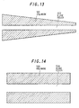
- FIG.14 shows the pattern of the second SiO 2 mask 505 for selective growth which is seen from a position over the wafer.
- a blank region 509 between the second SiO 2 masks 505 for selective growth has a width broader than that of the first SiO 2 mask 501 for selective growth.
- a p-buried cladding layer 207 with a thickness of 1.6 ⁇ m and a carrier concentration of 5x10 17 cm -3 , a p-InGaAs capping layer 208 with a thickness of 0.25 ⁇ m and a carrier concentration of 1x10 19 cm -3 are formed(FIG.12E).
- a polyimide film 301 with a thickness of 3 ⁇ m is formed thereon(FIG.12F).
- FIG.15 is a cross sectional view of the fabricated device cut along the line B-B' in FIG.11.
- the absorption-edge wavelength ⁇ g is set to be gradually changed from the long-wave side to the short-wave side along the direction of waveguiding light. Therefore, a sudden change of the absorption-edge wavelength in the optical absorption layer can be relaxed and reflection of a light wave or a radiation loss due to mode mismatching inside the optical absorption layer can be reduced as well as performing a negative chirping operation without applying a pre-bias.
- the modulator module 618 for optical communications comprises the semiconductor electroabsorption-type optical modulator 619 in the first or second embodiment on a sub-mount 617, spherical lenses 612, 612 and optical fibers 613, 613.
- the module 619 By using the module 619, a high-speed transmission of optical signal with a low insertion loss and a low chirp can be performed.
- a transmitter includes a light source 621 for inputting a light to the modulator module 618 for optical communications and a drive system 622 for driving the modulator module 618 and the light source 621.
- the light from the light source 621 is converted into an optical signal by the modulator module 618 for optical communications, transmitted through an optical fiber 623, and detected by a light-receiving unit 625 of a receiver 624.
- the electroabsorption-type optical modulator in which the negative chirping modulation can be performed without applying a constant bias and without increasing an absorption loss in the ON state of light, can be obtained without requiring the complicated fabrication process and with a good yield.
- the optical absorption waveguide of the electroabsorption-type optical modulator when the optical absorption waveguide of the electroabsorption-type optical modulator is fabricated, it can be formed by patterning the thin dielectric film such as SiO 2 to provide a mask for the selective growth and conducting the selective crystal growth, without using any etching process of semiconductor.
- the region needs only to be sandwiched with the SiO 2 mask.
- the thin dielectric film over the broad area with a good reproducibility is much easier than to etch a semiconductor up to an order of ⁇ m.
Landscapes
- Physics & Mathematics (AREA)
- Nonlinear Science (AREA)
- General Physics & Mathematics (AREA)
- Optics & Photonics (AREA)
- Optical Modulation, Optical Deflection, Nonlinear Optics, Optical Demodulation, Optical Logic Elements (AREA)
- Optical Integrated Circuits (AREA)
- Optical Communication System (AREA)
- Semiconductor Lasers (AREA)
Description
- This invention relates to a semiconductor optical modulator, and more particularly to, an electroabsorption-type optical modulator in which the absorption of a light wave supplied is controlled by changing an intensity of electric field applied to a semiconductor optical absorption layer, and relates to a method for making the same.
- Recently, with the development of high-speed and long-distance optical communication systems, there occurs a problem in conventional direct modulation manners with semiconductor lasers. Namely, in the semiconductor laser direct modulation manners, wavelength chirping occurs when the modulation is conducted, thereby the waveform after transmitting through an optical fiber is deteriorated. This phenomenon is amplified with an increase in signal modulation frequency or transmission distance. Especially, in a system that uses a conventional 1.3 µm zero-dispersion fiber, this problem is serious. Even if a light source with a wavelength band of 1.55 µm that has a small fiber propagation loss is used to increase the transmission distance, the transmission distance is limited by a dispersion limitation due to the chirping.
- This problem can be solved by an external modulation manner that modulates light emitted from a semiconductor laser by an external optical modulator other than the semiconductor laser while keeping the semiconductor laser emitting the light with a constant optical output. Therefore, external optical modulators has been increasingly developed. The external optical modulators can be composed of dielectric materials such as LiNbO3 or semiconductor materials such as InP, GaAs. In particular, semiconductor optical modulators are attractive since they can be integrated with optical elements such as a semiconductor laser, an optical amplifier or electronic circuits such as FET and can be easily miniaturized and operated with a reduced voltage.
- The semiconductor optical modulators include absorption-type optical modulators in which the intensity modulation is conducted by varying an optical absorption coefficient based on an effect that the absorption edge is shifted to a long-wave end by applying an electric field, e.g., a Franz-Keldish effect in bulk semiconductor or a quantum cofined Stark effect in multiquantum well(MQW), and Mach-Zehnder-type modulators which utilize a refractive index variation caused by an electrooptic effect(Pockels effect) or the quantum confined effect in bulk semiconductor.
- In the Mach-Zehnder-type modulators, in principle, the chirping can be reduced to zero. However, since they have a interference-type structure, a simple linear waveguide structure as in the absorption-type modulators cannot be obtained, therefore its fabrication and operation are complicated. On the other hand, in the absorption-type modulators, the wavelength chirping is much lower than that of the semiconductor laser direct modulation manner, but it cannot be reduced to zero. In electroabsorption-type optical modulators, when an electric field corresponding to an electrical signal is applied to an optical absorption layer, the absorption coefficient for an incident light with a wavelength (λop) longer than the absorption-edge wavelength of the optical absorption layer of the modulator is increased to extinguish the incident light. FIG.1 shows detuning Δλ(a difference between the wavelength of an incident light and the absorption-edge wavelength of the optical absorption layer) and applied electric field dependencies of the absorption coefficient. By setting the detuning to be a proper value, a good extinction characteristic can be obtained. Thus, an external electrical signal can be converted into ON/OFF of light. In this case, the refractive index of the optical absorption layer to the incident light also varies as shown in FIG.2. Namely, when the intensity of the electric field varies from zero to a value to conduct the absorption modulation, the refractive index of the optical absorption layer also varies. The magnitude of chirping when conducting ON/OFF of light is proportional to the ratio Δn/Δα of a refractive index variation Δn to an absorption variation Δα. Therefore, since Δn≥0 and Δα≥0 are usually obtained, a positive chirping occurs. However, if the difference between the wavelength of an incident light, λop and the absorption-edge wavelength of the optical absorption layer, λg, i.e., detuning Δλop (=λop - λg) is decreased, Δn≤0 and Δα≥0 can be satisfied, therefore allowing a negative chirping operation. But, since the absorption coefficient is increased, a sufficient light output cannot be obtained in the ON state of light. Recently, it has been experimentally proved that the chirping can be reduced by superposing a signal electric field corresponding to an electrical signal after applying a constant electric field to an electroabsorption-type optical modulator. Such an electroabsorption-type optical modulator has been expected to be a modulator for ultra-high speed and long distance optical communications in the future.
- For example, such an electroabsorption-type optical modulator is reported in K. Yamada et al.,"Low-Chirp, Low-Polarization Dependent Characteristics of Electroabsorption Optical Intensity Modulator with an InGaASP Bulk", The Institute of Electronics Information and Information Engineers(IEICE), 1995 General Meeting, annex paper vol.1, p.349(lecture No. C-349). In this report, it is described that the fiber dispersion durability in 10 Gb/s transmission and 1.55 µm wavelength can be enhanced by superposing an electrical signal after applying a constant bias to the modulator to overcome the dispersion limitation due to the transmission distance. Also, K. Morito et al.,"10Gb/s Transmission over 100 km of Standard Fiber with a Blue Chirp", IEICE, 1995 Electronics Society Meeting, annex paper vol.1, p.301(lecture No.C-301) reports an example of an electroabsorption optical modulator with a MQW structure, which is integrated with a DFB laser. In this report, it is described that the dispersion durability in 10Gb/s-100 km transmission can be enhanced by previously applying a constant bias of 1.1 V to the modulator.
- As described above, the pre-bias applying techniques where a constant bias is previously applied to the electroabsorption-type optical modulator have merits that the chirping can be reduced and the limitation to the transmission distance due to the dispersion can be overcome. However, there occur problems that the emission power in the ON state of light is decreased and the extinction ratio is deteriorated when the pre-bias is applied. Furthermore, a drive circuit(bias T circuit) for applying a constant bias to an external electrical signal as shown in FIG.3 is required.
- GB-PS 2 243 456 shows an electroabsorption optical modulator according to the preamble part of claim 1.
- Accordingly, it is an object of the invention to provide an electroabsorption-type optical modulator in which a negative chirp during a modulation can be obtained without previously applying a constant bias and a sufficient light emission power and a good distinction ratio can be obtained.
- This object is solved by the features of claim 1.
- The dependent claims show advantageous embodiments of the invention.
- An electroabsorption-type optical modulator, comprises:
- a semiconductor substrate; and
- a semiconductor buffer layer, a semiconductor optical absorption layer and a semiconductor cladding layer which are layered in this order on the semiconductor substrate;
- wherein the absorption of a light wave supplied to an end of the semiconductor optical absorption layer is controlled by changing an intensity of electric field applied to the semiconductor optical absorption layer;
- the semiconductor optical absorption layer has a region with absorption-edge wavelength shorter than that of the other region of the semiconductor optical absorption layer and a voltage corresponding an external electrical signal is simultaneously applied to both the regions of the semiconductor optical absorption layer, so that, to an incident light, a refractive index of the semiconductor optical absorption layer is decreased and an absorption coefficient of the semiconductor optical absorption layer is increased when an intensity of electric field applied to the semiconductor optical absorption layer corresponding to the external electrical signal is increased.
-
- An electroabsorption-type optical modulator, comprises:
- a semiconductor substrate; and
- a semiconductor buffer layer, a semiconductor optical absorption layer and a semiconductor cladding layer which are layered in this order on the semiconductor substrate;
- wherein the absorption of a light wave supplied to an end of the semiconductor optical absorption layer is controlled by changing an intensity of electric field applied to the semiconductor optical absorption layer; and
- the semiconductor optical absorption layer has absorption-edge wavelengths which continuously vary along the direction of waveguiding an incident light from a short-wave side to a long-wave side or from a long-wave side to a short-wave side, so that, to an incident light, a refractive index of the semiconductor optical absorption layer is decreased and an absorption coefficient of the semiconductor optical absorption layer is increased when an intensity of electric field applied to the semiconductor optical absorption layer corresponding to the external electrical signal is increased.
-
- An electroabsorption-type optical modulator, comprises:
- a semiconductor substrate; and
- a semiconductor buffer layer, a semiconductor optical absorption layer and a semiconductor cladding layer which are layered in this order on the semiconductor substrate;
- wherein the absorption of a light wave supplied to an end of the semiconductor optical absorption layer is controlled by changing an intensity of electric field applied to the semiconductor optical absorption layer; and
- the semiconductor optical absorption layer has absorpticn-edge wavelengths which vary stepwise along the direction of waveguiding an incident light, so that, to an incident light, a refractive index of the semiconductor optical absorption layer is decreased and an absorption coefficient of the semiconductor optical absorption layer is increased when an intensity of electric field applied to the semiconductor optical absorption layer corresponding to the external electrical signal is increased.
-
- A method for making a semiconductor optical modulator, comprises the steps of:
- forming a first semiconductor buffer layer on a semiconductor substrate;
- forming a first dielectric mask for selective growth on the first semiconductor buffer layer, the first dielectric mask including two regions in which a dielectric mask width is partially varied and a blank region sandwiched by the two regions;
- forming a second semiconductor buffer layer, a semiconductor optical absorption layer and a semiconductor cladding layer in this order on the blank region;
- forming a second dielectric mask for selective growth which has a blank region broader than the blank region of the first dielectric mask;
- forming a semiconductor cladding layer and a semiconductor capping layer in this order on the blank region of the second dielectric mask for selective growth;
- forming a first dielectric protective film over the entire top surface of the substrate;
- forming a second dielectric protective film on the first dielectric protective film;
- removing the first dielectric protective film and the second dielectric protective film until the semiconductor capping layer is exposed;
- forming an electrode for applying an electric field to the semiconductor optical absorption layer on the semiconductor capping layer; and
- removing the second dielectric protective film except under the electrode; wherein the electrode on the semiconductor capping layer is formed all over the semiconductor optical absorption layer, so that a voltage corresponding to an external signal is uniformly applied to the semiconductor optical absorption layer.
-
- According to a further aspect of the invention, an optical communication module, comprises:
- the electroabsorption-type optical modulator defined in claim 1;
- a first light-condensing means for optically coupling an input light to the semiconductor optical absorption layer of the electroabsorption-type optical modulator; and
- a second light-condensing means for optically coupling a light output from the semiconductor optical absorption layer to an external optical fiber.
-
- According to a further aspect of the invention, an optical communication system, comprises:
- a transmitter which includes the electroabsorption-type optical modulator defined in claim 1;
- means for externally waveguiding a light output from the transmitter; and
- a receiver for receiving the light output from the waveguiding means.
-
- In this invention, the semiconductor electroabsorption-type optical modulator has an optical absorption layer with a plurality of regions with different absorption-edge wavelengths along the direction of waveguiding a light, i.e., the optical absorption layer includes a region where a absorption-edge wavelength is shifted to a long-wave side rather than usual. Therefore, when a uniform electric field is applied to the regions, as the entire modulator, the refractive index is varied to a negative direction and the absorption coefficient is increased. Also, the ratio of lengths of the short-wave side and the long-wave side of the absorption layer is properly determined so that the absorption coefficient of the entire absorption layer is sufficiently small when no bias is applied. Thus, a negative chirp during a modulation can be obtained without previously applying a constant bias and a sufficient light emission power and a good extinction ratio can be obtained.
- To provide such a structure, this invention employs a bandgap control technique using a selective MOVPE(metal organic vapor phase epitaxy) method. According as each of the widths of dielectric mask regions on both sides of the blank region is partially varied, the absorption-edge wavelength of the optical absorption layer is partially varied. By using the crystal growth method, the optical absorption layer with partially different absorption-edge wavelengths can be formed in one growth step, i.e., it is not necessary to repeat an etching and a crystal growth for divided regions. Therefore, an electroabsorption-type optical modulator can be made with a good uniformity, reproducibility and controllability.
- The invention will be explained in more detail in conjunction with the appended drawings, wherein:
- FIG.1 shows the detuning and applied electric field dependencies of an absorption coefficient of the optical absorption layer in a conventional electroabsorption-type optical modulator,
- FIG.2 shows detuning and applied electric field dependencies of the refractive index of the optical absorption layer in a conventional electrcabsorption-type optical modulator,
- FIG.3 is a block diagram showing a driving method in conventional electroabsorption-type optical modulators,
- FIG.4 is a perspective view showing a InP-system MQW electroabsorption-type optical modulator in a first preferred embodiment of the invention,
- FIGS.5A to 5H are cross sectional views showing a method for making the InP-system MQW electroabsorption-type optical modulator in the first embodiment,
- FIG.6 is a plan view showing an example of a first mask pattern for selective growth used to make the InP-system MQW electroabsorption-type optical modulator in the first embodiment,
- FIG.7 is a plan view showing an example of a second mask pattern for selective growth used to make the InP-system MQW electroabsorption-type optical modulator in the first embodiment,
- FIG.8 shows the detuning and applied electric field dependencies of an absorption coefficient of an optical absorption layer in the InP-system MQW electroabsorption-type optical modulator in the first embodiment,
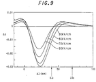
- FIG.9 shows detuning and applied electric field dependencies of an refractive index of the optical absorption layer in the InP-system MQW electroabsorption-type optical modulator in the first embodiment,
- FIG.10 is a longitudinal sectional view cut along the line B-B' in FIG.4,
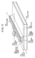
- FIG.11 is a perspective view showing a InP-system MQW electroabsorption-type optical modulator in a second preferred embodiment of the invention,
- FIGS.12A to 12H are cross sectional views showing a method for making the InP-system MQW electroabsorption-type optical modulator in the second embodiment,
- FIG.13 is a plan view showing an example of a first mask pattern for selective growth used to make the InP-system MQW electroabsorption-type optical modulator in the second embodiment,
- FIG.14 is a plan view showing an example of a second mask pattern for selective growth used to make the InP-system MQW electroabsorption-type optical modulator in the second embodiment,
- FIG.15 is a longitudinal sectional view cut along the line B-B' in FIG.11,
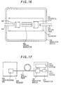
- FIG.16 is an illustration showing an optical communication module, which includes an electroabsorption-type optical modulator, in a third preferred embodiment of the invention, and
- FIG.17 is an illustration showing an optical communication system, which includes an optical communication module with an electroabsorption-type optical modulator, in a fourth preferred embodiment of the invention.
-
- A InP-system multiquantum well(MQW) electroabsorption-type optical modulator and a method for making the same in the first preferred embodiment will be explained in FIGS.4, 5A to 5H, 6, 7 and 10.
- FIGS.5A to 5H show a method for making the InP-system multiquantum well(MQW) electroabsorption-type optical modulator, wherein FIGS.5A to 5H are cross sectional views cut along the line A-A' in FIG.4.
- First, a n-InP buffer layer 102 with a thickness of 0.8 µm and a carrier concentration of 1x1017 cm-3 is formed on the entire surface of a (100) direction n-InP substance 101(FIG.5A). Then, a SiO2 film with a thickness of 1000 Å to provide a dielectric mask for selective growth is grown thereon, patterning the SiO2 film by using a standard photolithography technique, thereby forming a first SiO2 mask 201 for selective growth(FIG.5B). FIG.6 shows the pattern of the first SiO2 mask 201 for selective growth which is seen from a position over the wafer. In a blank region 302 which is sandwiched between two regions of the SiO2 mask 201, an absorption layer of the electroabsorption-type optical modulator is formed. In the blank region 302, the absorption layer for a long-wave side absorption-edge wavelength corresponding to the narrow-width area of the SiO2 mask 201 and the absorption layer for a short-wave side absorption-edge wavelength corresponding to the broad-width area of the SiO2 mask 201 are formed. Next, by using the selective MOVPE(metal organic vapor phase epitaxy) crystal growth method with the SiO2 mask, a n-InP cladding layer 202 with a thickness of 700 Å and a carrier concentration of 1x1017 cm-3, a MQW optical absorption layer 203(eighteen periods of InGaAsP(6nm)/InGaAsP(5.8nm)) with a thickness of 2124 Å and a carrier concentration of 5x1015 cm-3 and a p-InP cladding layer 204 with a thickness of 1600 Å and a carrier concentration of 5x1017 cm-3 are formed in this order(FIG.5C). Then, a SiO2 film is formed on the entire surface of the wafer, subsequently forming a second SiO2 mask 205 for selective growth which is used to bury the optical absorption layer by the photolithography(FIG.5D). FIG.7 shows the pattern of the second SiO2 mask 205 for selective growth which is seen from a position over the wafer. A blank region 209 between the second SiO2 masks 205 for selective growth has a width broader than that of the first SiO2 mask 201 for selective growth. Then, by using the selective MOVPE crystal growth method with the second SiO2 mask 205 for selective growth, a p-buried cladding layer 207 with a thickness of 1.6 µm and a carrier concentration of 5x1017 cm-3, a p-InGaAs capping layer 208 with a thickness of 0.25 µm and a carrier concentration of 1x1019 cm-3 are formed(FIG.5E). Then, after forming a SiO2 protective film 300 with a thickness of 1000 Å on the entire surface of the wafer, a polyimide film 301 with a thickness of 3 µm is formed thereon(FIG.5F). Then, uniformly removing the polyimide film 301 and the SiO2 protective film 300 until the p-InGaAs capping layer 208 is exposed, a p-electrode 401 of Cr/Au is formed(FIG.5G). Then, the polyimide film 301 except under the p-electrode 401 is removed, and a n-electrode 402 of Cr/Au(FIG.5H) is formed. Finally, cleaving the device, conducting a reflectionless coating on the end surfaces for the emission and incidence of light, the device fabrication is completed. FIG.10 is a cross sectional view of the fabricated device cut along the line B-B' in FIG.4. The absorption-edge wavelength λg1 in region 1 is set to be longer than the absorption-edge wavelength λg2 in region 2.
- The operation of the InP-system MQW electroabsorption-type optical modulator fabricated by the above process will be explained below. A light wave with a wavelength of 1.55 µm supplied to the InP-system MQW electroabsorption-type optical modulator shown in FIG.4 is emitted substantially without being absorbed when an external bias of 0V is applied to the modulator(light ON state), and it is absorbed to extinguish the light when an external bias of 2V is applied(light OFF state). In this regard, variations of the absorption coefficient and the refractive index in the long-wave and short-wave sides of the optical absorption layer of the electroabsorption-type -type optical modulator are shown in FIGS.8 and 9. The electric field intensities of 0 kV/cm to 90 kV/cm correspond to the applied signal biases 0V to 2V, and the variation of refractive index Δn1 is -0.013 to the short-wave side detuning(difference between the incident light wavelength and the absorption-edge wavelength of the optical absorption layer) Δλ1=40 nm and the variation of refractive index Δn2 is 0.0025 to the long-wave side detuning Δλ2=70 nm. The waveguide length of the short-wave side optical absorption layer L1 is 30 µm and the waveguide length of the long-wave side optical absorption layer L2 is 150 µm. The phase variation ΔΦ of an incident light caused by the signal bias change from the OFF state to the ON state is given by:
- The parameter α that represents the chirping is given by:
- Though the absorption coefficient in the ON state(applied signal bias of 0V) is increased according as the detuning is shifted to the short-wave side, the absorption loss in the ON state can be suppressed to be substantially small since the waveguide length L1 (=30 µm) of the optical absorption layer with the short-wave side detuning in the electroabsorption-type optical modulator is sufficiently short.
- As explained above, in the first embodiment, the negative chirping modulation operation can be performed without previously applying a DC bias and without causing an increase in absorption loss.
- Meanwhile, in the electroabsorption-type optical modulator shown in FIG.4, since the polyimide film 301 is thick buried under the pad, the pad capacity can be reduced. Thus, by using the reduction technique of the electrode capacity, the electroabsorption-type optical modulator in the first embodiment can be used for such a high-speed modulation as 10 Gb/s.
- The invention is not limited to the above embodiment, where the InP-system MQW structure electroabsorption-type optical modulator is used, and may employ a InGaAs/InP MQW or a Al-system MQW. Also, the invention is not limited to the device form, for example, the thicknesses and compositions of the respective layers(films) or the dimension of the waveguide, in the first embodiment.
- A InP-system multiquantum well(MQW) electroabsorption-type optical modulator and a method for making the same in the second preferred embodiment will be explained in FIGS.11, 12A to 12H and 13 to 15.
- FIGS.12A to 12H show a method for making the InP-system multiquantum well(MQW) electroabsorption-type optical modulator, wherein FIGS.12A to 12H are cross sectional views cut along the line A-A' in FIG.11.
- First, a n-InP buffer layer 102 with a thickness of 0.8 µm and a carrier concentration of 1x1017 cm-3 is formed on the entire surface of a (100) direction n-InP substance 101(FIG.12A). Then, a SiO2 film with a thickness of 1000 Å to provide a dielectric mask for selective growth is grown thereon, patterning the SiO2 film by using a standard photolithography technique, thereby forming a first SiO2 mask 501 for selective growth(FIG.12B). FIG.13 shows the pattern of the first SiO2 mask 501 for selective growth which is seen from a position over the wafer. In a blank region 502 which is sandwiched between two regions of the SiO2 mask 501, an absorption layer of the electroabsorpticn-type optical modulator is formed. In the region 502, on both sides of which the width of the SiO2 mask 501 is decreased along the direction of waveguiding light, the absorption layer for a long-wave side absorption-edge wavelength corresponding to the narrow-width area of the SiO2 mask 501 and the absorption layer for a short-wave side absorption-edge wavelength corresponding to the broad-width area of the SiO2 mask 501 are formed. Next, by using the selective MOVPE crystal growth method with the SiO2 mask, a n-InP cladding layer 202 with a thickness of 700 Å and a carrier concentration of 1x1017 cm-3, a MQW optical absorption layer 203(eighteen periods of InGaAsP(6nm)/InGaAsP(5.8nm)) with a thickness of 2124 Å and a carrier concentration of 5x1015 cm-3 and a p-InP cladding layer 204 with a thickness of 1600 Å and a carrier concentration of 5x1017 cm-3 are formed in this order(FIG.12C). Then, a SiO2 film is formed on the entire surface of the wafer, subsequently forming a second SiO2 mask 505 for selective growth which is used to bury the optical absorption layer by the photolithography(FIG.12D). FIG.14 shows the pattern of the second SiO2 mask 505 for selective growth which is seen from a position over the wafer. A blank region 509 between the second SiO2 masks 505 for selective growth has a width broader than that of the first SiO2 mask 501 for selective growth. Then, by using the selective MOVPE crystal growth method with the second SiO2 mask 505 for selective growth, a p-buried cladding layer 207 with a thickness of 1.6 µm and a carrier concentration of 5x1017 cm-3, a p-InGaAs capping layer 208 with a thickness of 0.25 µm and a carrier concentration of 1x1019 cm-3 are formed(FIG.12E). Then, after forming a SiO2 protective film 300 with a thickness of 1000 Å on the entire surface of the wafer, a polyimide film 301 with a thickness of 3 µm is formed thereon(FIG.12F). Then, uniformly removing the polyimide film 301 and the SiO2 protective film 300 until the p-InGaAs capping layer 208 is exposed, a p-electrode 401 of Cr/Au is formed(FIG.12G). Then, the polyimide film 301 except under the p-electrode 401 is removed, and a n-electrode 402 of Cr/Au(FIG.12H) is formed. Finally, cleaving the device, conducting a reflectionless coating on the end surfaces for the emission and incidence of light, the device fabrication is completed. FIG.15 is a cross sectional view of the fabricated device cut along the line B-B' in FIG.11. The absorption-edge wavelength λg is set to be gradually changed from the long-wave side to the short-wave side along the direction of waveguiding light. Therefore, a sudden change of the absorption-edge wavelength in the optical absorption layer can be relaxed and reflection of a light wave or a radiation loss due to mode mismatching inside the optical absorption layer can be reduced as well as performing a negative chirping operation without applying a pre-bias.
- An optical communication module in the third preferred embodiment of the invention will be explained in FIG.16. As shown, the modulator module 618 for optical communications comprises the semiconductor electroabsorption-type optical modulator 619 in the first or second embodiment on a sub-mount 617, spherical lenses 612, 612 and optical fibers 613, 613. By using the module 619, a high-speed transmission of optical signal with a low insertion loss and a low chirp can be performed.
- An optical communication system for trunk line system in the fourth preferred embodiment of the invention, which adopts the modulator module 618 for optical communications, will be explained in FIG.17. As shown, a transmitter includes a light source 621 for inputting a light to the modulator module 618 for optical communications and a drive system 622 for driving the modulator module 618 and the light source 621. The light from the light source 621 is converted into an optical signal by the modulator module 618 for optical communications, transmitted through an optical fiber 623, and detected by a light-receiving unit 625 of a receiver 624. By using the optical communication system in the fourth embodiment, a repeater-free optical transmission further than 100 km can be easily realized. This is because the signal deterioration caused by the dispersion in the optical fiber 623 can be significantly suppressed due to the occurrence of a negative direction chirping.
- As described above, according to the invention, the electroabsorption-type optical modulator, in which the negative chirping modulation can be performed without applying a constant bias and without increasing an absorption loss in the ON state of light, can be obtained without requiring the complicated fabrication process and with a good yield. In the invention, when the optical absorption waveguide of the electroabsorption-type optical modulator is fabricated, it can be formed by patterning the thin dielectric film such as SiO2 to provide a mask for the selective growth and conducting the selective crystal growth, without using any etching process of semiconductor.
- Furthermore, to change the absorption-edge wavelength of the optical absorption layer in a specific region, the region needs only to be sandwiched with the SiO2 mask. To finely pattern the thin dielectric film over the broad area with a good reproducibility is much easier than to etch a semiconductor up to an order of µm. Thus, by using the method of the invention, the electroabsorption-type optical modulator with partial different absorption-edge wavelengths can be produced with a good reproducibility.
- Although the invention has been described with respect to specific embodiment for complete and clear disclosure, the appended claims are not to be thus limited but are to be construed as embodying all modification and alternative constructions that may be occurred to one skilled in the art which fairly fall within the basic teaching here is set forth.
Claims (9)
- An electroabsorption-type optical modulator, comprising:wherein the absorption of a light wave supplied to an end of said semiconductor optical absorption layer (203) is controlled by changing the intensity of an electric field applied to said semiconductor optical absorption layer;a semiconductor substrate (101); anda semiconductor buffer layer (102), a semiconductor optical absorption layer (203) and a semiconductor cladding layer (204) which are layered in this order on said semiconductor substrate (101);
characterized in that
said semiconductor optical absorption layer (203) has a plurality of regions with different absorption-edge wavelengths along the direction of waveguiding an incident light;
wherein the semiconductor optical absorption layer (203) is adapted to respond to an incident light in such a way that a refractive index of said semiconductor optical absorption layer is decreased and an absorption coefficient of said semiconductor optical absorption layer is increased when the intensity of said electric field applied to said semiconductor optical absorption layer corresponding to said external electrical signal is increased. - An electroabsorption-type optical modulator according to claim 1, wherein:said semiconductor optical absorption layer has a region with absorption-edge wavelength shorter than that of the other region of said semiconductor optical absorption layer and a voltage corresponding an external electrical signal is simultaneously applied to both said regions of said semiconductor optical absorption layer.
- An electroabsorption-type optical modulator according to claim 1, wherein:
said semiconductor optical absorption layer has absorption-edge wavelengths which continuously vary along the direction of waveguiding an incident light from a short-wave side to a long-wave side or from a long-wave side to a short-wave side. - An electroabsorption-type optical modulator according to claim 1, wherein:
said semiconductor optical absorption layer has absorption-edge wavelengths which vary stepwise along the direction of waveguiding an incident light. - An electroabsorption-type optical modulator, according to any of claims 1 to 4, wherein:
said semiconductor optical absorption layer (203) is composed of a multiquantum well structure. - A method for making a semiconductor optical modulator, comprising the steps of:wherein said electrode on said semiconductor capping layer is formed all over said semiconductor optical absorption layer, so that a voltage corresponding to an external signal is uniformly applied to said semiconductor optical absorption layer;forming a first semiconductor buffer layer on a semiconductor substrate;forming a first dielectric mask for selective growth on said first semiconductor buffer layer, said first dielectric mask including two regions in which a dielectric mask width is partially varied and a blank region sandwiched by said two regions;forming a second semiconductor buffer layer, a semiconductor optical absorption layer and a semiconductor cladding layer in this order on said blank region;forming a second dielectric mask for selective growth which has a blank region broader than said blank region of said first dielectric mask;forming a semiconductor cladding layer and a semiconductor capping layer in this order on said blank region of said second dielectric mask for selective growth;forming a first dielectric protective film over the entire top surface of said substrate;forming a second dielectric protective film on said first dielectric protective film;removing said first dielectric protective film and said second dielectric protective film until said semiconductor capping layer is exposed;forming an electrode for applying an electric field to said semiconductor optical absorption layer on said semiconductor capping layer; andremoving said second dielectric protective film except under said electrode;
wherein the length of each region is chosen such that in response to an incident light a refractive index of said semiconductor optical absorption layer is decreased and an absorption coefficient of said semiconductor optical absorption layer is increased than an intensity of an electric field applied to said semiconductor optical absorption layer corresponding to said external electrical signal is increased. - A method for making a semiconductor optical modulator, according to claim 6, wherein:
said semiconductor optical absorption layer is composed of a multiquantum well structure. - An optical communication module, comprising:said electroabsorption-type optical modulator defined by any of claims 1 to 4;a first light-condensing means for optically coupling an input light to said semiconductor optical absorption layer of said electroabsorption-type optical modulator; anda second light-condensing means for optically coupling a light output from said semiconductor optical absorption layer to an external optical fiber.
- An optical communication system, comprising:a transmitter which includes said electroabsorption-type optical modulator defined by any of claims 1 to 4;means for externally waveguiding a light output from said transmitter; anda receiver for receiving said light output from said waveguiding means.
Applications Claiming Priority (3)
| Application Number | Priority Date | Filing Date | Title |
|---|---|---|---|
| JP8127497A JP2955986B2 (en) | 1996-05-22 | 1996-05-22 | Semiconductor optical modulator and method of manufacturing the same |
| JP127497/96 | 1996-05-22 | ||
| JP12749796 | 1996-05-22 |
Publications (3)
| Publication Number | Publication Date |
|---|---|
| EP0809129A2 EP0809129A2 (en) | 1997-11-26 |
| EP0809129A3 EP0809129A3 (en) | 1998-05-06 |
| EP0809129B1 true EP0809129B1 (en) | 2002-01-02 |
Family
ID=14961439
Family Applications (1)
| Application Number | Title | Priority Date | Filing Date |
|---|---|---|---|
| EP97108311A Expired - Lifetime EP0809129B1 (en) | 1996-05-22 | 1997-05-22 | Semiconductor optical modulator and method for making the same |
Country Status (4)
| Country | Link |
|---|---|
| US (2) | US6150667A (en) |
| EP (1) | EP0809129B1 (en) |
| JP (1) | JP2955986B2 (en) |
| DE (1) | DE69709436T2 (en) |
Families Citing this family (39)
| Publication number | Priority date | Publication date | Assignee | Title |
|---|---|---|---|---|
| JP2817713B2 (en) * | 1996-06-17 | 1998-10-30 | 日本電気株式会社 | Semiconductor optical modulator |
| JPH1096879A (en) * | 1996-09-20 | 1998-04-14 | Nec Corp | Semiconductor optical modulator and optical communication device using the same |
| US6310902B1 (en) * | 1998-04-29 | 2001-10-30 | Agere Systems Optoelectronics Guardian Corp. | Modulator for analog applications |
| SE522417C2 (en) | 1998-10-15 | 2004-02-10 | Ericsson Telefon Ab L M | Electro-absorption modulator (EAM) and method for manufacturing such modulator |
| US6528337B1 (en) * | 1999-04-08 | 2003-03-04 | The Furukawa Electric Co., Ltd. | Process of producing semiconductor layer structure |
| JP4656459B2 (en) * | 1999-12-02 | 2011-03-23 | Okiセミコンダクタ株式会社 | Semiconductor optical functional device and semiconductor optical functional element |
| JP2001274510A (en) * | 2000-03-28 | 2001-10-05 | Toshiba Corp | Waveguide type optical device and method of manufacturing the same |
| US6597718B2 (en) * | 2000-07-18 | 2003-07-22 | Multiplex, Inc. | Electroabsorption-modulated fabry perot laser |
| US7031612B2 (en) | 2000-07-18 | 2006-04-18 | Multiplex, Inc. | Optical transponders and transceivers |
| US6754243B2 (en) | 2000-08-09 | 2004-06-22 | Jds Uniphase Corporation | Tunable distributed feedback laser |
| US6459521B1 (en) * | 2000-08-28 | 2002-10-01 | Agere Systems Guardian Corp. | Electroabsorption modulator integrated distributed feedback laser transmitter |
| JP2002072010A (en) * | 2000-09-05 | 2002-03-12 | Nippon Sheet Glass Co Ltd | Optical device having wavelength selectivity |
| US6376795B1 (en) * | 2000-10-24 | 2002-04-23 | Lsi Logic Corporation | Direct current dechucking system |
| US6847060B2 (en) * | 2000-11-27 | 2005-01-25 | Kopin Corporation | Bipolar transistor with graded base layer |
| US7345327B2 (en) * | 2000-11-27 | 2008-03-18 | Kopin Corporation | Bipolar transistor |
| AU2002219895A1 (en) * | 2000-11-27 | 2002-06-03 | Kopin Corporation | Bipolar transistor with lattice matched base layer |
| US6800879B2 (en) | 2001-01-08 | 2004-10-05 | Kopin Corporation | Method of preparing indium phosphide heterojunction bipolar transistors |
| JP2002222989A (en) * | 2001-01-26 | 2002-08-09 | Toshiba Corp | Semiconductor light emitting device |
| WO2002080317A1 (en) | 2001-03-30 | 2002-10-10 | Santur Corporation | Alignment of an on chip modulator |
| US6922278B2 (en) | 2001-03-30 | 2005-07-26 | Santur Corporation | Switched laser array modulation with integral electroabsorption modulator |
| US6781734B2 (en) | 2001-03-30 | 2004-08-24 | Santur Corporation | Modulator alignment for laser |
| AU2002254522A1 (en) | 2001-03-30 | 2003-11-11 | Santur Corporation | High speed modulation of arrayed lasers |
| DE10128655B4 (en) * | 2001-06-15 | 2005-12-15 | Orga Kartensysteme Gmbh | Smart card with optical modulator and method for transmitting information from a smart card |
| US6944197B2 (en) * | 2001-06-26 | 2005-09-13 | University Of Maryland, Baltimore County | Low crosstalk optical gain medium and method for forming same |
| US7120183B2 (en) * | 2001-07-11 | 2006-10-10 | Optium Corporation | Electro-absorption modulated laser with high operating temperature tolerance |
| SE520139C2 (en) | 2001-11-30 | 2003-06-03 | Optillion Ab | Laser modulator with electrically separated laser and modulator sections |
| US20050141800A1 (en) * | 2002-09-17 | 2005-06-30 | Mitsubishi Denki Kabushiki Kaisha | Waveguide semiconductor optical device and process of fabricating the device |
| JP2004109312A (en) * | 2002-09-17 | 2004-04-08 | Mitsubishi Electric Corp | Waveguide type semiconductor optical device and method of manufacturing the same |
| JP4030847B2 (en) * | 2002-09-20 | 2008-01-09 | ユーディナデバイス株式会社 | Semiconductor photo detector |
| US7098149B2 (en) * | 2003-03-04 | 2006-08-29 | Air Products And Chemicals, Inc. | Mechanical enhancement of dense and porous organosilicate materials by UV exposure |
| TWI240959B (en) | 2003-03-04 | 2005-10-01 | Air Prod & Chem | Mechanical enhancement of dense and porous organosilicate materials by UV exposure |
| US7573928B1 (en) | 2003-09-05 | 2009-08-11 | Santur Corporation | Semiconductor distributed feedback (DFB) laser array with integrated attenuator |
| JP2005175295A (en) * | 2003-12-12 | 2005-06-30 | Hitachi Ltd | Semiconductor optical device and optical module |
| JP2006032623A (en) * | 2004-07-15 | 2006-02-02 | Sharp Corp | Manufacturing method of semiconductor laser device |
| GB2417126A (en) * | 2004-08-09 | 2006-02-15 | Qinetiq Ltd | Method for fabricating lateral semiconductor device |
| US7102807B2 (en) * | 2004-10-19 | 2006-09-05 | National Central University | High-speed electro-absorption modulator with low drive voltage |
| US7566948B2 (en) | 2004-10-20 | 2009-07-28 | Kopin Corporation | Bipolar transistor with enhanced base transport |
| JP6610044B2 (en) * | 2014-07-14 | 2019-11-27 | 住友電気工業株式会社 | Semiconductor optical modulator and manufacturing method of semiconductor optical modulator |
| CN113608371B (en) * | 2021-07-13 | 2024-03-19 | 厦门大学 | An infrared electric absorption modulator based on type II broken bandgap quantum well |
Family Cites Families (23)
| Publication number | Priority date | Publication date | Assignee | Title |
|---|---|---|---|---|
| US3295911A (en) * | 1963-03-15 | 1967-01-03 | Bell Telephone Labor Inc | Semiconductor light modulators |
| JPS61212823A (en) * | 1985-03-18 | 1986-09-20 | Nec Corp | Optical modulator |
| JPH0650366B2 (en) * | 1985-06-28 | 1994-06-29 | 日本電気株式会社 | Light modulator |
| JPH0827446B2 (en) * | 1986-02-18 | 1996-03-21 | 日本電信電話株式会社 | Quantum well type optical modulator and manufacturing method thereof |
| JPH03293622A (en) * | 1990-04-12 | 1991-12-25 | Hitachi Ltd | Optical modulator |
| US5227648A (en) * | 1991-12-03 | 1993-07-13 | Woo Jong Chun | Resonance cavity photodiode array resolving wavelength and spectrum |
| DE69331979T2 (en) * | 1992-02-28 | 2003-01-23 | Hitachi, Ltd. | Optical integrated semiconductor device and method for manufacturing and use in a light receiver |
| JP3223562B2 (en) * | 1992-04-07 | 2001-10-29 | 株式会社日立製作所 | Optical transmission device, optical transmission device, and optical modulator |
| JPH06214169A (en) * | 1992-06-08 | 1994-08-05 | Texas Instr Inc <Ti> | Controllable optical and periodic surface filter |
| EP0582078B1 (en) * | 1992-08-05 | 2000-08-16 | Motorola, Inc. | Superluminescent edge emitting device |
| JPH06181366A (en) * | 1992-12-14 | 1994-06-28 | Fujitsu Ltd | Optical semiconductor device |
| EP0606093B1 (en) * | 1993-01-07 | 1997-12-17 | Nec Corporation | Semiconductor optical integrated circuits and method for fabricating the same |
| FR2707766B1 (en) * | 1993-07-02 | 1995-12-08 | Fabrice Devaux | Electroabsorbent modulator and optical pulse generator comprising it. |
| JP2669335B2 (en) * | 1993-12-20 | 1997-10-27 | 日本電気株式会社 | Semiconductor light source and manufacturing method thereof |
| JPH07230066A (en) * | 1994-02-18 | 1995-08-29 | Hitachi Ltd | Semiconductor optical modulator |
| JPH07234389A (en) * | 1994-02-22 | 1995-09-05 | Hitachi Ltd | Semiconductor optical device |
| JP2982619B2 (en) * | 1994-06-29 | 1999-11-29 | 日本電気株式会社 | Semiconductor optical waveguide integrated photodetector |
| JP2842292B2 (en) * | 1994-09-16 | 1998-12-24 | 日本電気株式会社 | Semiconductor optical integrated device and manufacturing method |
| JPH08146365A (en) * | 1994-11-16 | 1996-06-07 | Nec Corp | Semiconductor mach-zehnder modulation device and its production |
| US5937273A (en) * | 1994-12-27 | 1999-08-10 | Fujitsu Limited | Fabricating compound semiconductor by varying ratio of stagnant layer thickness and mean free path of seed material |
| GB2302738B (en) * | 1995-06-28 | 1999-03-03 | Northern Telecom Ltd | Semiconductor modulator with a shift |
| US5838052A (en) * | 1996-03-07 | 1998-11-17 | Micron Technology, Inc. | Reducing reflectivity on a semiconductor wafer by annealing titanium and aluminum |
| US5771257A (en) * | 1996-12-26 | 1998-06-23 | Mitsubishi Denki Kabushiki Kaisha | Light absorption modulator and integrated semiconductor laser and modulator |
-
1996
- 1996-05-22 JP JP8127497A patent/JP2955986B2/en not_active Expired - Fee Related
-
1997
- 1997-05-21 US US08/859,896 patent/US6150667A/en not_active Expired - Lifetime
- 1997-05-22 DE DE69709436T patent/DE69709436T2/en not_active Expired - Fee Related
- 1997-05-22 EP EP97108311A patent/EP0809129B1/en not_active Expired - Lifetime
-
2000
- 2000-08-21 US US09/643,158 patent/US6426236B1/en not_active Expired - Lifetime
Also Published As
| Publication number | Publication date |
|---|---|
| JPH09311304A (en) | 1997-12-02 |
| EP0809129A2 (en) | 1997-11-26 |
| US6150667A (en) | 2000-11-21 |
| EP0809129A3 (en) | 1998-05-06 |
| DE69709436D1 (en) | 2002-02-07 |
| JP2955986B2 (en) | 1999-10-04 |
| US6426236B1 (en) | 2002-07-30 |
| DE69709436T2 (en) | 2002-08-22 |
Similar Documents
| Publication | Publication Date | Title |
|---|---|---|
| EP0809129B1 (en) | Semiconductor optical modulator and method for making the same | |
| US5799119A (en) | Coupling of strongly and weakly guiding waveguides for compact integrated mach zehnder modulators | |
| EP2458433B1 (en) | Optical modulator and manufacturing method of the optical modulator | |
| US6778309B2 (en) | Electroabsorption modulator with tunable chirp | |
| US5048907A (en) | Electric field induced quantum well waveguides | |
| US5801872A (en) | Semiconductor optical modulation device | |
| US8600198B2 (en) | Semiconductor optical modulator, semiconductor optical integrated device, and method of manufacturing the same | |
| US4837526A (en) | Semiconductor external optical modulator | |
| US5757985A (en) | Semiconductor mach-zehnder-type optical modulator | |
| US5655034A (en) | Mach-Zehnder type modulator and method of driving the same | |
| US6222966B1 (en) | Adiabatic Y-branch waveguide having controllable chirp | |
| JP2817602B2 (en) | Semiconductor Mach-Zehnder modulator and method of manufacturing the same | |
| KR100500097B1 (en) | Optical modulator | |
| US6064788A (en) | Adiabatic Y-branch modulator with negligible chirp | |
| US5953149A (en) | Semiconductor electroabsorption optical modulator | |
| JPH09293927A (en) | Optical integrated semiconductor laser | |
| US6115169A (en) | Semiconductor optical modulator and integrated optical circuit device | |
| US5999298A (en) | Electroabsorption optical intesity modulator having a plurality of absorption edge wavelengths | |
| JP2000258739A (en) | Optical modulator and light source for optical communication | |
| JPH09101491A (en) | Semiconductor mach-zehnder modulator and its production | |
| US20050141072A1 (en) | Electroabsorption modulator with two sections | |
| JP2000241775A (en) | Optical modulator, light source for optical communication and module for optical communication |
Legal Events
| Date | Code | Title | Description |
|---|---|---|---|
| PUAI | Public reference made under article 153(3) epc to a published international application that has entered the european phase |
Free format text: ORIGINAL CODE: 0009012 |
|
| AK | Designated contracting states |
Kind code of ref document: A2 Designated state(s): DE FR GB |
|
| PUAL | Search report despatched |
Free format text: ORIGINAL CODE: 0009013 |
|
| AK | Designated contracting states |
Kind code of ref document: A3 Designated state(s): DE FR GB |
|
| 17P | Request for examination filed |
Effective date: 19980408 |
|
| 17Q | First examination report despatched |
Effective date: 19991201 |
|
| GRAG | Despatch of communication of intention to grant |
Free format text: ORIGINAL CODE: EPIDOS AGRA |
|
| GRAH | Despatch of communication of intention to grant a patent |
Free format text: ORIGINAL CODE: EPIDOS IGRA |
|
| GRAH | Despatch of communication of intention to grant a patent |
Free format text: ORIGINAL CODE: EPIDOS IGRA |
|
| GRAA | (expected) grant |
Free format text: ORIGINAL CODE: 0009210 |
|
| REG | Reference to a national code |
Ref country code: GB Ref legal event code: IF02 |
|
| AK | Designated contracting states |
Kind code of ref document: B1 Designated state(s): DE FR GB |
|
| REF | Corresponds to: |
Ref document number: 69709436 Country of ref document: DE Date of ref document: 20020207 |
|
| ET | Fr: translation filed | ||
| PLBE | No opposition filed within time limit |
Free format text: ORIGINAL CODE: 0009261 |
|
| STAA | Information on the status of an ep patent application or granted ep patent |
Free format text: STATUS: NO OPPOSITION FILED WITHIN TIME LIMIT |
|
| 26N | No opposition filed | ||
| PGFP | Annual fee paid to national office [announced via postgrant information from national office to epo] |
Ref country code: DE Payment date: 20070517 Year of fee payment: 11 |
|
| PGFP | Annual fee paid to national office [announced via postgrant information from national office to epo] |
Ref country code: GB Payment date: 20070516 Year of fee payment: 11 |
|
| PGFP | Annual fee paid to national office [announced via postgrant information from national office to epo] |
Ref country code: FR Payment date: 20070510 Year of fee payment: 11 |
|
| GBPC | Gb: european patent ceased through non-payment of renewal fee |
Effective date: 20080522 |
|
| REG | Reference to a national code |
Ref country code: FR Ref legal event code: ST Effective date: 20090119 |
|
| PG25 | Lapsed in a contracting state [announced via postgrant information from national office to epo] |
Ref country code: FR Free format text: LAPSE BECAUSE OF NON-PAYMENT OF DUE FEES Effective date: 20080602 Ref country code: DE Free format text: LAPSE BECAUSE OF NON-PAYMENT OF DUE FEES Effective date: 20081202 |
|
| PG25 | Lapsed in a contracting state [announced via postgrant information from national office to epo] |
Ref country code: GB Free format text: LAPSE BECAUSE OF NON-PAYMENT OF DUE FEES Effective date: 20080522 |