EP0803883A1 - Transformateur de convertisseur - Google Patents
Transformateur de convertisseur Download PDFInfo
- Publication number
- EP0803883A1 EP0803883A1 EP97106164A EP97106164A EP0803883A1 EP 0803883 A1 EP0803883 A1 EP 0803883A1 EP 97106164 A EP97106164 A EP 97106164A EP 97106164 A EP97106164 A EP 97106164A EP 0803883 A1 EP0803883 A1 EP 0803883A1
- Authority
- EP
- European Patent Office
- Prior art keywords
- primary
- winding
- wound
- chambers
- windings
- Prior art date
- Legal status (The legal status is an assumption and is not a legal conclusion. Google has not performed a legal analysis and makes no representation as to the accuracy of the status listed.)
- Granted
Links
Images


Classifications
-
- H—ELECTRICITY
- H01—ELECTRIC ELEMENTS
- H01F—MAGNETS; INDUCTANCES; TRANSFORMERS; SELECTION OF MATERIALS FOR THEIR MAGNETIC PROPERTIES
- H01F38/00—Adaptations of transformers or inductances for specific applications or functions
- H01F38/42—Flyback transformers
Definitions
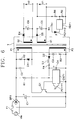
- the present invention relates to a converter transformer used in a switching regulator or the like employing the circuit of a fly-back converter.
- the circuit of a fly-back converter of a general type has a converter transformer T, an input rectifying circuit BR1 for rectifying an input voltage Vin, a fuse F1, a drive-control and overvoltage protection circuit CNT1, a photo coupler consisting of a light emitting element PC1-2 and a light receiving element PC1-1, a main switching element Q1, an output detecting circuit REF1, resistors R1 to R7, capacitors C1 to C6, diodes D1 to D4, an inductor L1, and the like.
- This transformer T has primary windings consisting of a primary excitation winding P1 and a primary auxiliary winding P2 and secondary windings consisting of a secondary winding S1 for producing a main operating voltage and another secondary winding S2 for producing another operating voltage.
- the AC input Vin is rectified by the input rectifying circuit BR1 and is smoothed by the capacitor C1 to be converted to a DC voltage.
- This DC voltage is the input voltage of the converter transformer.
- the capacitor C4 is charged by a starting current flowing through the starting resistor R1 to actuate the drive-control and overvoltage protection circuit CNT1. Then, the main switch Q1 is turned on, and an input voltage is impressed on the primary excitation winding P1 of the converter transformer T. In this state, the diodes D2, D3 and D4 are turned off, and all energy supplied to the primary excitation winding P1 is accumulated in the converter transformer T.
- the main switching element Q1 is turned off, and the diodes D2, D3 and D4 are turned on.
- the energy accumulated in the converter transformer T is supplied from the primary auxiliary winding P2 to the power source voltage side of the drive-control and overvoltage protection circuit CNT1 and is discharged from the secondary winding S1 which produces the main operating voltage and another secondary winding S2 which produces another operating voltage to the secondary output side.
- the on/off drive control of the main switching element Q1 is made in the following way.
- the output detecting circuit REF1 connected to the output side of the secondary winding S1 which produces the main operating voltage detects the output voltage of the secondary winding S1 which produces the main operating voltage.
- the detected signal is fed back to the drive-control and overvoltage protection circuit CNT1 through the photo coupler consisting of the light emitting element PC1-2 and the light receiving element PC1-1.
- the fed-back signal from the drive-control and overvoltage protection circuit CNT1 controls the drive of the main switching element Q1 connected to the primary excitation winding P1 so that the output voltage of the secondary winding S1 which produces the main operating voltage is stabilized.
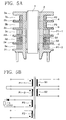
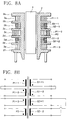
- the conventional converter transformer which operates by means of a fly-back converter circuit or the like has a structure as shown in Figs. 7A and 7B or Figs. 8A and 8B.
- Figs. 7A and 7B are shown a cross-sectional view and a circuit diagram of one of the conventional converter transformers, respectively.
- the transformer includes a bobbin 2 having a magnetic core 1 inserted therein and a plurality of flanges 2a to 2d formed thereon. Chambers 3a to 3c are individually defined between the adjacent flanges 2a to 2d on the bobbin 2.
- the primary excitation windings consist of a primary excitation winding P1-1 wound on a chamber 3a and another primary excitation winding P1-2 wound on another chamber 3c.
- the primary auxiliary winding P2 which is one of the primary windings is wound on the outer periphery of the primary excitation winding P1-1.
- the second windings S1 and S2 are wound in an overlapping manner on the chamber 3b between the chambers 3a and 3c on which the primary excitation windings P1-1 and P1-2 are wound individually. This arrangement ensures the electrical insulation satisfying the safety standard.
- the primary exaltation windings P1-1 and P1-2 are individually wound on the different chambers 3a and 3c, and the secondary windings S1 and S2 are wound on the chamber 3b between the chambers 3a and 3c, as described above.
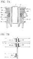
- Figs. 8A and 8B are shown a cross sectional view and a circuit diagram of another conventional converter transformer.
- the primary windings P1 and secondary windings S1 and S2 are divided into the primary windings P1-1, P1-2 and P1-3 and the secondary windings S1-1, S1-2, S2-1, and S2-2 which are more than those of the transformer as shown in Figs. 7A and 7B.
- the primary windings P1-1, P1-2 and P1-3 are connected in series and wound on every other chambers 3a, 3c and 3e, respectively.
- a pair of the secondary windings S1-1 and S1-2 are connected in series, whereas another pair of the secondary windings S2-1 and S2-2 are connected in parallel.
- the secondary windings S1-1 and S1-2 are wound on the chamber 3b between the chambers 3a and 3c and on the chamber 3d between the chambers 3c and 3e, respectively. Further, the secondary windings S2-1 and S2-2 are wound around the secondary winding S1-1 on the chamber 3b and around the secondary winding S1-2 on the chamber 3d, respectively.
- the primary auxiliary winding P2 is wound on the outer periphery of one of the so-divided primary windings P1-2.
- the primary auxiliary winding P2 is an important winding which provides an electric power to the drive-control and overvoltage protection circuit CNT1 to control the main switching element Q1 as shown in Fig. 6.
- the spike voltage Vs produced in the primary auxiliary winding P2 upon turning the main switching element Q1 off is large as shown in Fig. 9, the fly-back converter circuit cannot be controlled stably with the result that the main switching element Q1 cannot operate suitably or the overvoltage protection circuit portion assembled in the fly-back converter circuit operates erroneously.
- the inductor L1, the resistor R4 and the like be connected in series to the primary auxiliary winding P2, or a snubber circuit consisting of the resistor R3 and the capacitor C3 be connected in parallel to the primary auxiliary winding P2.
- An object of the present invention is to provide a fly-back converter transformer used in a fly-back converter, in which the spike voltage produced in the primary auxiliary winding can be reduced to simplify the snubber circuit.
- Another object of the present invention is provide a converter transformer which has no circuit components for suppressing the spike voltage of the primary auxiliary winding or uses only a small number of such circuit components for suppressing the spike voltage, resulting in the reduction of the number of components of the transformer and miniaturization of the components, thereby lowering the cost of the transformer.
- a further object of the present invention is to provide a converter transformer in which extremely high electrical insulation is achieved between the primary auxiliary winding and the primary excitation windings whereby the reliability of the transformer is improved.
- a still further object of the present invention is to provide a converter transformer in which the spike voltage is extremely reduced when the load current is zero or very small.
- the converter transformer in an aspect of the present invention comprises a bobbin made of resin and having an outer periphery and at least four flanges formed in tandem on the outer periphery, at least three chambers defined between the adjacent flanges, a primary auxiliary winding for supplying electric power to a drive-control and overvoltage protection circuit, the primary auxiliary winding being wound on one of the chambers, a primary excitation winding wound on another of the chambers, which is separated by one or two chambers from the primary auxiliary windings, at least one secondary winding which always consumes electric power and which is wound on one of the chambers between the primary auxiliary winding and the primary excitation winding.
- the primary auxiliary winding is not wound on the primary excitation winding but is wound on a chamber which is separated by one or two cambers (hereinafter referred to as the "intermediate chamber") from the chamber on which the primary excitation winding is wound.
- This arrangement weakens the magnetic connection between the primary excitation winding and the primary auxiliary winding. Since the secondary winding or primary winding which always exhausts electric power is wound on the intermediate chamber, the magnetic connection between the primary auxiliary winding and the winding wound on the intermediate chamber is enhanced, and existence of the winding on the intermediate chamber further weakens the magnetic connection between the primary excitation winding and the primary auxiliary winding. Thus, the spike voltage produced in the primary auxiliary winding can be reduced.
- the reduction of the spike voltage allows for easy control of the fly-back converter circuit and prevents the overvoltage protection circuit from operating erroneously.
- the circuit components for suppressing the spike voltage can be eliminated or the number of such components can be reduced.
- the number of the components is reduced and/or the components can be miniaturized. This leads to the lowering of the cost of the transformer.
- the electrical insulation between the primary auxiliary winding and the primary excitation winding is remarkably improved, and thus the reliability of the transformer can be enhanced.
- a converter transformer comprising a bobbin made of resin and having an outer periphery and at five flanges formed in tandem on the outer periphery; at least four chambers defined between the adjacent flanges; a primary auxiliary winding for supplying electric power to a drive-control and overlvoltage protection circuit, the primary auxiliary winding being wound on one of the chambers; a primary excitation winding wound on another of the chambers, which is separated by one or two chambers from the primary auxiliary winding; at least one secondary winding divided into at least two divided windings, one of the divided endings being wound on the chamber between the primary auxiliary winding and the primary excitation winding, and the other of the divided windings being wound on one of the chambers other than the chambers on which the primary auxiliary winding, the primary excitation ending and said one of the divided windings are wound; and said one of the divided windings being connected in parallel to at least one of the other of the divided windings.
- FIG. 1A is a cross-sectional view
- Fig. 1B which is a circuit diagram.
- the transformer has a magnetic core 1 and a bobbin 2 into which the magnetic core 1 is inserted.
- Flanges 2a to 2f are formed in tandem on the outer periphery of the bobbin 2.
- Chambers 3a to 3e are separately defined between the adjacent flanges 2a to 2f so as to be provided separately from each other.
- Primary excitation windings comprise two divided primary excitation windings P1-1 and P1-2 wound on the chambers 3c and 3e.
- the chambers 3a, 3c and 3e are arranged with chambers 3b and 3d disposed therebetween.
- the divided primary excitation windings P1-1 and P1-2 are connected in series. However, they may be connected in parallel, instead.
- a secondary winding S1 which produces the main operating voltage is not divided but is wound on one of the chambers 3d.
- a secondary winding S2 which produces another operating voltage is not divided and wound on the chamber 3b disposed between the chambers 3a and 3c on which the primary auxiliary winding P2 and the primary excitation winding P1-1 are wound.
- To the secondary winding S2 is connected a dummy or a load 4 which always exhausts the electric power so that the secondary winding S2 always exhausts the electric power.
- the primary auxiliary winding P2 is not wound on the primary excitation winding P1-1 or P1-2 but is wound on the chamber 3a which is disposed separately from the chambers 3c and 3e on which the primary excitation windings P1-1 and P1-2 are wound. Owing to this arrangement, the magnetic connection between the primary exaltation windings P1-1 and P1-2 and the primary auxiliary winding P2 is weakened.
- the primary auxiliary winding P2 is wound on the chamber 3a disposed adjacent to the chamber 3b on which the second winding S2 always exhausting the electric power is wound.
- the magnetic connection between the primary auxiliary winding P2 and the secondary winding S2 is strong, and the magnetic connection between the primary auxiliary winding P2 and the primary excitation winding P1-1 is weakened further, whereby the spike voltage Vs as shown in Fig. 9 can be reduced. Reduction of the spike voltage Vs allows for easy control of the fly-back converter circuit and prevents erroneous operation of the overvoltage protection circuit.
- the capacitor C3 and the resistor R3 can be removed or reduced in number.
- the number of components of the transformer can be reduced and/or the components can be miniaturized, leading to the reduction of the cost of the transformer.
- the primary auxiliary winding P2 and the primary excitation windings P1-1 and P1-2 are wound on the different chambers 3a, 3c and 3e, the electrical insulation between the primary auxiliary winding P2 and the primary excitation windings P1-1 and P1-2 is remarkably improved, thereby enhancing the reliability of the transformer.
- the secondary winding S1 is wound on the chamber 3d between the chambers3c and 3e on which the divided primary excitation windings P1-1 and P1-2 are wound, the leakage inductance between the windings P1-1, P1-2 and S1 can be reduced thereby lowering the spike voltage produced in these windings.
- the primary excitation windings consist of only two divided primary exaltation windings P1-1 and P1-2.
- the number of the windings of the converter transformer is limited to a minimum, so that a small and inexpensive converter transformer in which the number of the terminal pins of the converter transformer is limited to a minimum is provided.
- Figs. 2A and 2B are a cross-sectional view and a circuit diagram of a second embodiment of the present invention.
- This embodiment has four chambers 3a to 3d defined between the flanges 2a to 2e.
- a primary excitation winding P1 is not divided and is wound only one chamber 3c, whereas the secondary windings which produce the main operating voltage consist of two divided secondary windings S1-1 and S1-2 and are wound on the chambers 3b and 3d on both sides of the chamber 3c for the primary excitation winding P1.
- the chamber 3b for one of the divided secondary windings, S1-1 is arranged adjacent to the chamber 3a on which the primary auxiliary winding P2 is wound and the divided secondary windings S1-1 and S1-2 are connected in parallel.
- a secondary winding S2 which produces another operating voltage is wound on the outer periphery of the divided secondary winding S1-2.
- the arrangement of the secondary winding S1-1 on the chamber 3b between the primary auxiliary winding P2 and the primary excitation winding P1 weakens the magnetic connection between the primary auxiliary winding P2 and the primary excitation winding P1. Even if a specific load does not exist, parallel connection between the divided secondary windings S1-1 and S1-2 causes a reactive current to flow through the windings S1-1 and S1-2 due to the difference of inductances produced from the difference of the winding positions or the like of the windings S1-1 and S1-2. Thus, the magnetic connection between the primary excitation winding P1 and the primary auxiliary winding P2 is reduced further so that the spike voltage Vs is remarkably reduced. Similarly to the case of the embodiment as shown in Fig.
- the arrangement of the primary winding P1 between the secondary windings S1-1 and S1-2 can reduce the leakage inductance, whereby the spike voltages produced in the windings P1, S1-1 and S1-2 can be reduced. Further, because the secondary winding are divided into only two secondary windings S1-1 and S1-2 , the number of the windings of the convert transformer is limited to a minimum. Thus, a small and inexpensive converter transformer in which the number of the terminal pins of the converter transformer is also limited to a minimum can be provided.
- Figs. 3A and 3B are a cross-sectional view and a circuit diagram of a third embodiment according to the present invention.
- the secondary windings S2 which produce another operating voltage also comprise two secondary windings S2-1 and S2-2 and a pair of the secondary windings S1-1 and S2-1 are wound on a chamber 3b so that the one overlaps on the other, that the primary auxiliary winding P2 and the primary excitation winding P1 are arranged on both sides of the secondary windings S1-1 and S2-1, respectively, and that the other pair of the secondary winding sections S1-2 and S2-2 are wound on a chamber 3d so that the one overlaps on the other.
- the fly-back converter can be controlled easily, the overvoltage protection circuit can be prevented from operating erroneously, the number of the members such as the snubber circuit can be reduced, the parts can be made small and the converter transformer can be manufactured at a low cost. Since the primary auxiliary winding P2 and the primary excitation winding P1 are wound on the different chambers 3a and 3c, the electrical insulation between the primary auxiliary winding P2 and the primary excitation winding P1 is remarkably enhanced, resulting in high reliability.
- the arrangement of the primary excitation winding P1 between the secondary windings S1-1 and S1-2 strengthens the magnetic connection therebetween and can reduce the leakage inductance therebetween.
- the spike voltages produced in the windings P1, S1-1 and S1-2 can also be reduced.
- the second windings consist of the secondary windings S1-1 and S1-2 which produce the main operating voltage and the secondary windings S2-1 and S2-2, whereas the primary excitation winding P is not divided.
- the primary excitation winding P1 as shown in Fig. 8
- the number of the windings of the converter transformer is reduced and the number of the terminal pins of the converter transformer is also made smaller, whereby a small and inexpensive converter transformer can be provided.
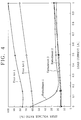
- Fig. 4 are illustrated the comparative relationships of the load currents versus the spike voltage ratios between the first to third embodiments (indicated as Embodiment 1,. Embodiment 2 and Embodiment 3, respectively) and the two cases of prior art (i.e., Prior Art 1 as shown in Figs. 7A and 7B and Prior Art 2 as shown in Figs. 8A and 8B).
- the tests were made under the conditions in which the input AC voltage of the present invention and the prior art is 100V, the output voltages V1 and V2 of the secondary windings S1 and S2 are 14V and 6.5V, respectively.
- the spike voltage Vs of the present invention is reduced to about one-third of the prior art 1 and 2.
- the spike voltage Vs is rapidly reduced as the load current increases within the rage of the load current of 0A to substantially 0.2A.
- a reactive current flows even if no load is connected. When the load current is zero, therefore, the spike voltage Vs is much lower than that of the prior art.
- the secondary winding S2, S1-1 or S2-1 which always consumes the electric power is provided on the chamber 3b between the primary auxiliary winding P2 and the primary excitation winding P1 or the primary excitation winding P1-1.
- a primary winding P3, which is other than primary excitation winding P1 and the primary auxiliary winding P2 and which always consumes the electric power may be provided on the chamber 3b which is between the chamber 3a of the primary auxiliary winding P2 and the chamber 3c of the primary excitation winding P1-1.
- a plurality of chambers may be provided between the primary auxiliary winding P2 and the primary excitation winding P1-1 or the primary excitation winding P1, and primary windings or the secondary windings which always consume the electric power may be wound on thereon.
- the chambers 3a to 3e are individually manufactured and may have connecting faces a to d as those of the fourth embodiment shown in Fig. 5A, and the adjacent connecting faces a to d of the chambers 3a to 3e may be adhered to each other or fitted together or fastened together by means of connecting members.
Applications Claiming Priority (3)
| Application Number | Priority Date | Filing Date | Title |
|---|---|---|---|
| JP13083196 | 1996-04-27 | ||
| JP8130831A JP2974967B2 (ja) | 1996-04-27 | 1996-04-27 | コンバータトランス |
| JP130831/96 | 1996-04-27 |
Publications (2)
| Publication Number | Publication Date |
|---|---|
| EP0803883A1 true EP0803883A1 (fr) | 1997-10-29 |
| EP0803883B1 EP0803883B1 (fr) | 1999-09-08 |
Family
ID=15043725
Family Applications (1)
| Application Number | Title | Priority Date | Filing Date |
|---|---|---|---|
| EP97106164A Expired - Lifetime EP0803883B1 (fr) | 1996-04-27 | 1997-04-15 | Transformateur de convertisseur |
Country Status (5)
| Country | Link |
|---|---|
| US (2) | US6075431A (fr) |
| EP (1) | EP0803883B1 (fr) |
| JP (1) | JP2974967B2 (fr) |
| DE (1) | DE69700485T2 (fr) |
| MY (1) | MY126309A (fr) |
Cited By (3)
| Publication number | Priority date | Publication date | Assignee | Title |
|---|---|---|---|---|
| WO2007085372A1 (fr) * | 2006-01-26 | 2007-08-02 | Pilz Gmbh & Co. Kg | Dispositif de commutation de sécurité et procédé d'arrêt sécurisé d'un récepteur électrique |
| US7948345B2 (en) | 2008-02-06 | 2011-05-24 | Murata Manufacturing Co., Ltd. | Transformer and transformer device |
| CN104103408A (zh) * | 2013-04-02 | 2014-10-15 | 宝辉科技(龙南)有限公司 | 变压器 |
Families Citing this family (24)
| Publication number | Priority date | Publication date | Assignee | Title |
|---|---|---|---|---|
| JPH10163044A (ja) * | 1996-12-02 | 1998-06-19 | Matsushita Electric Ind Co Ltd | コンバータトランス |
| JP3072261U (ja) * | 2000-04-04 | 2000-10-06 | 船井電機株式会社 | 巻線部品 |
| JP2002008924A (ja) * | 2000-06-20 | 2002-01-11 | Cosel Co Ltd | トランス実装構造及びトランス |
| US6597593B1 (en) * | 2000-07-12 | 2003-07-22 | Sun Microsystems, Inc. | Powering IC chips using AC signals |
| US20020053901A1 (en) * | 2000-10-05 | 2002-05-09 | Strayer Lance Ronald | Linear inductive fluid level sensor |
| KR20030007422A (ko) * | 2000-12-14 | 2003-01-23 | 코닌클리케 필립스 일렉트로닉스 엔.브이. | 과전압 보호를 하는 고전압 변압기, 및 과전압 보호 방법 |
| JP4678988B2 (ja) * | 2001-06-05 | 2011-04-27 | 新電元工業株式会社 | スイッチング電源 |
| DE10135599A1 (de) * | 2001-07-20 | 2003-02-13 | Thomson Brandt Gmbh | Schaltnetzteil mit Powerfaktorkorrektur, sowie Spule für eine diesbezügliche Korrekturschaltung |
| JP2004128160A (ja) * | 2002-10-01 | 2004-04-22 | Murata Mfg Co Ltd | 高圧トランス |
| DE10257908A1 (de) * | 2002-12-11 | 2004-06-24 | Patent-Treuhand-Gesellschaft für elektrische Glühlampen mbH | Getaktete Leistungsversorgung |
| KR100560751B1 (ko) * | 2003-12-17 | 2006-03-13 | 삼성전자주식회사 | 정전 검출 장치 |
| TWM267472U (en) * | 2004-07-16 | 2005-06-11 | Logah Technology Corp | Air gap transformer for liquid crystal back light driver |
| US7940536B2 (en) * | 2006-05-30 | 2011-05-10 | International Rectifier Corporation | Flyback converter with improved synchronous rectification |
| CN101529536B (zh) * | 2006-10-31 | 2011-12-28 | 三菱电机株式会社 | 板型变压器及放电灯点亮装置 |
| JP5887700B2 (ja) * | 2011-03-07 | 2016-03-16 | 富士電機株式会社 | 高周波トランス |
| JP2013062399A (ja) * | 2011-09-14 | 2013-04-04 | Minebea Co Ltd | トランス |
| US8693219B2 (en) * | 2011-10-21 | 2014-04-08 | Wafly Ltd. | Power factor improvement circuit with phase adjustment and current gain reduction |
| KR101499720B1 (ko) * | 2013-08-30 | 2015-03-06 | 삼성전기주식회사 | 초크코일 및 이를 구비한 전원 공급 장치 |
| US10145873B2 (en) * | 2014-06-30 | 2018-12-04 | Rockwell Automation Technologies, Inc. | Coil architecture for inductive sensors |
| JP6165791B2 (ja) * | 2015-02-04 | 2017-07-19 | 株式会社タムラ製作所 | トランス及びスイッチング電源装置 |
| US10262789B2 (en) * | 2016-07-05 | 2019-04-16 | Tamura Corporation | Transformer and switched-mode power supply apparatus |
| US10249430B2 (en) * | 2016-07-05 | 2019-04-02 | Tamura Corporation | Transformer and switched-mode power supply apparatus |
| JP6428742B2 (ja) * | 2016-10-12 | 2018-11-28 | オムロン株式会社 | 変圧器およびそれを備えた電力変換器 |
| US10523088B2 (en) * | 2017-04-24 | 2019-12-31 | General Electric Company | Energy storage system for doubly fed induction generator |
Citations (1)
| Publication number | Priority date | Publication date | Assignee | Title |
|---|---|---|---|---|
| EP0071008A1 (fr) * | 1981-07-25 | 1983-02-09 | TELEFUNKEN Fernseh und Rundfunk GmbH | Transformateur de ligne, en particulier transformateur pour un récepteur de télévision |
Family Cites Families (14)
| Publication number | Priority date | Publication date | Assignee | Title |
|---|---|---|---|---|
| US3089081A (en) * | 1958-01-14 | 1963-05-07 | Schaevitz Engineering | Differential transformer |
| US4073003A (en) * | 1974-06-12 | 1978-02-07 | Raytheon Company | High efficiency low-loss power supply |
| EP0171690B1 (fr) * | 1984-08-16 | 1987-11-11 | TELEFUNKEN Fernseh und Rundfunk GmbH | Configuration de bobines avec noyau à cheville magnétisable |
| JPS6254409A (ja) * | 1985-09-03 | 1987-03-10 | Murata Mfg Co Ltd | ノイズ除去用インダクタ |
| US4968106A (en) * | 1987-12-04 | 1990-11-06 | Murata Manufacturing Co., Ltd. | High voltage generating apparatus for television equipment |
| NL8900509A (nl) * | 1989-03-02 | 1990-10-01 | Philips Nv | Geschakelde voedingsspanningsschakeling. |
| US4937727A (en) * | 1989-03-07 | 1990-06-26 | Rca Licensing Corporation | Switch-mode power supply with transformer-coupled feedback |
| JPH0648653B2 (ja) * | 1989-03-31 | 1994-06-22 | 日本ビクター株式会社 | フライバックトランス |
| JPH04133411A (ja) * | 1990-09-26 | 1992-05-07 | Taiyo Yuden Co Ltd | 柱状コンデンサ本体の製造方法 |
| JPH04354266A (ja) * | 1991-05-30 | 1992-12-08 | Sony Corp | 高圧安定化回路 |
| US5555494A (en) * | 1993-09-13 | 1996-09-10 | Morris; George Q. | Magnetically integrated full wave DC to DC converter |
| US5600293A (en) * | 1994-06-14 | 1997-02-04 | The United States Of America As Represented By The Secretary Of The Army | Integrated magnetic exploding foil initiator fire set |
| TW282594B (fr) * | 1994-06-30 | 1996-08-01 | Yokogawa Electric Corp | |
| US5576941A (en) * | 1994-08-10 | 1996-11-19 | York Technologies, Inc. | Modular power supply system |
-
1996
- 1996-04-27 JP JP8130831A patent/JP2974967B2/ja not_active Expired - Fee Related
-
1997
- 1997-04-15 DE DE69700485T patent/DE69700485T2/de not_active Expired - Lifetime
- 1997-04-15 EP EP97106164A patent/EP0803883B1/fr not_active Expired - Lifetime
- 1997-04-25 MY MYPI97001817A patent/MY126309A/en unknown
-
1998
- 1998-10-15 US US09/172,671 patent/US6075431A/en not_active Expired - Fee Related
-
1999
- 1999-01-25 US US09/236,370 patent/US5933332A/en not_active Expired - Lifetime
Patent Citations (1)
| Publication number | Priority date | Publication date | Assignee | Title |
|---|---|---|---|---|
| EP0071008A1 (fr) * | 1981-07-25 | 1983-02-09 | TELEFUNKEN Fernseh und Rundfunk GmbH | Transformateur de ligne, en particulier transformateur pour un récepteur de télévision |
Cited By (3)
| Publication number | Priority date | Publication date | Assignee | Title |
|---|---|---|---|---|
| WO2007085372A1 (fr) * | 2006-01-26 | 2007-08-02 | Pilz Gmbh & Co. Kg | Dispositif de commutation de sécurité et procédé d'arrêt sécurisé d'un récepteur électrique |
| US7948345B2 (en) | 2008-02-06 | 2011-05-24 | Murata Manufacturing Co., Ltd. | Transformer and transformer device |
| CN104103408A (zh) * | 2013-04-02 | 2014-10-15 | 宝辉科技(龙南)有限公司 | 变压器 |
Also Published As
| Publication number | Publication date |
|---|---|
| DE69700485D1 (de) | 1999-10-14 |
| MY126309A (en) | 2006-09-29 |
| US6075431A (en) | 2000-06-13 |
| EP0803883B1 (fr) | 1999-09-08 |
| US5933332A (en) | 1999-08-03 |
| JP2974967B2 (ja) | 1999-11-10 |
| JPH09293613A (ja) | 1997-11-11 |
| DE69700485T2 (de) | 2000-05-11 |
Similar Documents
| Publication | Publication Date | Title |
|---|---|---|
| US6075431A (en) | Converter transformer | |
| US11251713B2 (en) | Multiple parallel-connected resonant converter, inductor-integrated magnetic element and transformer-integrated magnetic element | |
| US7193496B2 (en) | Magnetic element and power supply | |
| US5932995A (en) | Dual buck converter with coupled inductors | |
| US20060221655A1 (en) | Filter circuit and power supply unit | |
| US20120119676A1 (en) | Flyback power converter with divided energy transfer element | |
| US11496064B2 (en) | Resonant converter and manufacturing method of transformer thereof | |
| US20120106207A1 (en) | Resonant transformer and resonant converter employing same | |
| US7184287B2 (en) | Rectifier clamping circuit with reverse energy recovery | |
| US5936857A (en) | Power converter having multiple output voltage capability | |
| US10917088B1 (en) | Power conversion device | |
| JP2005176535A (ja) | スイッチング電源装置 | |
| JP3201383B2 (ja) | 共振型電源用トランス | |
| US4660134A (en) | DC-DC converter with chopping switch and transformer | |
| KR100705856B1 (ko) | 미드포인트에서 피딩되는 정류기 | |
| JP3219726B2 (ja) | スイッチング電源装置 | |
| JP3405673B2 (ja) | 複数の異種電源を備えたフォワード・コンバータ | |
| JP2000299233A (ja) | 電源用トランス | |
| JP3207100B2 (ja) | トランスを有するdc−dcコンバ−タ | |
| JP2006318840A (ja) | 放電灯点灯装置 | |
| KR20220055746A (ko) | 전력 변환 장치 | |
| JP2003289670A (ja) | スイッチング電源 | |
| JP2749297B2 (ja) | フライバックトランス | |
| JPH1052043A (ja) | 絶縁型スイッチング電源 | |
| KR200156405Y1 (ko) | 핀타입 감압변압기 |
Legal Events
| Date | Code | Title | Description |
|---|---|---|---|
| PUAI | Public reference made under article 153(3) epc to a published international application that has entered the european phase |
Free format text: ORIGINAL CODE: 0009012 |
|
| AK | Designated contracting states |
Kind code of ref document: A1 Designated state(s): DE |
|
| 17P | Request for examination filed |
Effective date: 19980306 |
|
| 17Q | First examination report despatched |
Effective date: 19980408 |
|
| GRAG | Despatch of communication of intention to grant |
Free format text: ORIGINAL CODE: EPIDOS AGRA |
|
| GRAH | Despatch of communication of intention to grant a patent |
Free format text: ORIGINAL CODE: EPIDOS IGRA |
|
| GRAH | Despatch of communication of intention to grant a patent |
Free format text: ORIGINAL CODE: EPIDOS IGRA |
|
| GRAA | (expected) grant |
Free format text: ORIGINAL CODE: 0009210 |
|
| AK | Designated contracting states |
Kind code of ref document: B1 Designated state(s): DE |
|
| REF | Corresponds to: |
Ref document number: 69700485 Country of ref document: DE Date of ref document: 19991014 |
|
| PLBE | No opposition filed within time limit |
Free format text: ORIGINAL CODE: 0009261 |
|
| STAA | Information on the status of an ep patent application or granted ep patent |
Free format text: STATUS: NO OPPOSITION FILED WITHIN TIME LIMIT |
|
| 26N | No opposition filed | ||
| PGFP | Annual fee paid to national office [announced via postgrant information from national office to epo] |
Ref country code: DE Payment date: 20110413 Year of fee payment: 15 |
|
| REG | Reference to a national code |
Ref country code: DE Ref legal event code: R119 Ref document number: 69700485 Country of ref document: DE Effective date: 20121101 |
|
| PG25 | Lapsed in a contracting state [announced via postgrant information from national office to epo] |
Ref country code: DE Free format text: LAPSE BECAUSE OF NON-PAYMENT OF DUE FEES Effective date: 20121101 |