EP0802563A2 - Herstellungsverfahren für eine Halbleiteranordnung mit einer Metallsilizidschicht mit niedrigem Widerstand - Google Patents
Herstellungsverfahren für eine Halbleiteranordnung mit einer Metallsilizidschicht mit niedrigem Widerstand Download PDFInfo
- Publication number
- EP0802563A2 EP0802563A2 EP97106310A EP97106310A EP0802563A2 EP 0802563 A2 EP0802563 A2 EP 0802563A2 EP 97106310 A EP97106310 A EP 97106310A EP 97106310 A EP97106310 A EP 97106310A EP 0802563 A2 EP0802563 A2 EP 0802563A2
- Authority
- EP
- European Patent Office
- Prior art keywords
- heat treatment
- titanium
- manufacturing
- layer
- refractory metal
- Prior art date
- Legal status (The legal status is an assumption and is not a legal conclusion. Google has not performed a legal analysis and makes no representation as to the accuracy of the status listed.)
- Withdrawn
Links
Images


Classifications
-
- H—ELECTRICITY
- H10—SEMICONDUCTOR DEVICES; ELECTRIC SOLID-STATE DEVICES NOT OTHERWISE PROVIDED FOR
- H10D—INORGANIC ELECTRIC SEMICONDUCTOR DEVICES
- H10D30/00—Field-effect transistors [FET]
- H10D30/01—Manufacture or treatment
- H10D30/021—Manufacture or treatment of FETs having insulated gates [IGFET]
- H10D30/0223—Manufacture or treatment of FETs having insulated gates [IGFET] having source and drain regions or source and drain extensions self-aligned to sides of the gate
-
- H—ELECTRICITY
- H10—SEMICONDUCTOR DEVICES; ELECTRIC SOLID-STATE DEVICES NOT OTHERWISE PROVIDED FOR
- H10D—INORGANIC ELECTRIC SEMICONDUCTOR DEVICES
- H10D64/00—Electrodes of devices having potential barriers
- H10D64/01—Manufacture or treatment
- H10D64/011—Manufacture or treatment of electrodes ohmically coupled to a semiconductor
- H10D64/0111—Manufacture or treatment of electrodes ohmically coupled to a semiconductor to Group IV semiconductors
- H10D64/0112—Manufacture or treatment of electrodes ohmically coupled to a semiconductor to Group IV semiconductors using conductive layers comprising silicides
Definitions
- the present invention relates to a method of manufacturing a semiconductor device and, more specifically, to a method of forming a refractory metal silicide film in a self-aligned manner on a diffusion layer or gate electrode of a MOS transistor.
- MOS transistor fine structure insulating gate field effect transistor
- FIG. 9A A conventional method of manufacturing a MOS transistor having a self-aligned silicide structure is described with reference to Figs. 9A to 9C and Figs. 10A and 10B.
- Figs. 9A to 9C and Figs. 10A and 10B are sectional views of a MOS transistor showing the method of forming a self-aligned silicide.
- an element-separating insulating film 102 is formed in a predetermined region on a silicon substrate 101 by the well known LOCOS process.
- impurity ions are implanted as a channel stopper, and a gate insulating film 103 is formed by thermal oxidation.
- An about 150 nm-thick polysilicon film is then formed over the entire surface by CVD (chemical vapor deposition) and an impurity such as phosphorus is doped in the polysilicon film. Thereafter, this polysilicon film is patterned to a desired shape by photolithography and dry etching to form a gate electrode 104.
- a silicon oxide film is then formed over the entire surface by CVD and then anisotropic dry etching is carried out to form a spacer 105 on both side surfaces (sidewalls) of the gate electrode 104.
- impurity ions such as arsenic, boron or the like are implanted to form a diffusion layer 106 by heating at 800 to 1,000°C.
- impurity ions such as arsenic, boron or the like are implanted to form a diffusion layer 106 by heating at 800 to 1,000°C.
- the MOS transistor is of an N-channel type, a diffusion layer including arsenic is formed and when the MOS transistor is of a P-channel type, a diffusion layer including boron is formed.
- the diffusion layer 106 serves as source and drain regions of the transistor.
- an about 20 nm-thick titanium film 107 is formed over the entire surface by metal sputtering.
- a heat treatment is carried out in a nitrogen atmosphere for 30 to 60 sec.
- a lamp annealing device is generally used as a heat treatment device and treatment temperature is set to 600 to 650°C.
- titanium is silicificated.
- a crystalline C49-structured silicide layer 108 having a high electrical resistivity, a titanium layer containing nitrogen atoms, i.e., a nitrogen-containing titanium layer 109, and a nitrided titanium layer, i.e., a titanium nitride layer 110 are formed in that order on the exposed surface portion of the gate electrode 104 and the exposed surface portion of the diffusion layer 106.
- the nitrogen-containing titanium layer 109 and the titanium nitride layer 110 are formed in that order on the element-separated insulating film 102 which is a silicon oxide film and on the sidewall spacers 105.
- the above nitrogen-containing titanium layer 109 and the titanium nitride layer 110 are removed by a chemical solution prepared by a mixture of an ammonium aqueous solution, purified water and a hydrogen peroxide solution.
- the nitrogen-containing titanium film is dissolved in this chemical solution but the titanium nitride layer does not.
- the titanium nitride layer 110 is removed by lift-off caused by the dissolution of the nitrogen-containing titanium layer 109.
- the C49-structured silicide layer 108 is formed in a self-aligned manner only on the gate electrode 104 and the diffusion layer 106 for ource and drain regions.
- the heat treating device is the above-described lamp annealing device and the treatment temperature is set to 850°C.
- the above C49-structured silicide layer is converted into a different phase, i.e., the C54-structured silicide layer 111 having a low electrical resistivity.
- a C54-structured silicide layer containing nitrogen atoms i.e., a nitrogen-containing silicide layer 112 is formed.
- a refractory metal silicide film is formed in a self-aligned manner over the diffusion layer and gate electrode of the MOS transistor.
- Fig. 11 shows the temperature-time profile of the heat treatment step which is carried out by the conventional method.
- the semiconductor substrate in which the titanium layer is formed over semiconductor elements is inserted into a treatment chamber of the lamp annealing device and the atmosphere of the chamber is fully substituted with a nitrogen gas.
- the semiconductor substrate is heated to a predetermined temperature, 700°C in this case, by infrared lamp heating and maintained at that temperature for a predetermined time, 30 sec. in this case.
- the temperature of the semiconductor substrate is lowered by stopping the lamp heating.
- the semiconductor substrate is taken out from the lamp annealing device to complete the heat treatment step.
- the heat treatment step as shown in Fig. 9C, the crystalline C49-structured silicide layer 108 having a high electrical resistivity, the nitrogen-containing titanium layer 109 and the titanium nitride layer 110 are formed on the exposed surface portion of the gate electrode 104 and the exposed surface of the diffusion layer 106 of the semiconductor substrate.
- the nitrogen-containing titanium layer 109 and the titanium nitride layer 110 are formed on the element-separated insulating film 102 and the sidewall spacers 105.
- the above silicide formation technology of the conventional method involves the following problem when the line width of a gate electrode decreases along with a reduction in the design rule of semiconductor elements. That is, it is difficult to form a titanium silicide layer with a gate electrode line width of 0. 3 ⁇ m or less, whereby the resistance of electrode wiring increases. This is because most part of the titanium film is changed into titanium nitride and a titanium silicide layer is rarely formed because the silicification reaction rate in a thin line is slow ("thin line effect")and becomes slower than the nitriding reaction in the above conventional scheme of lamp annealing.
- the silicide layer When forming a silicide layer, the silicide layer must be selectively formed on the gate electrode and the diffusion layer only. In the formation of the silicide layer, the silicification reaction proceeds with silicon atoms being diffused into a layer of a refractory metal such as titanium.
- a silicide layer is formed even on the spacers which are silicon oxide films and the element-separated insulating film when silicon atoms originating in the diffusion layer or the polysilicon film are diffused into the refactory metal over the spacers or the element-separated insulating film (to be referred to as "overgrowth" hereinafter), thereby making impossible a selective formation of a silicide layer.
- overgrowth it is necessary to reduce the heat treatment temperature. At such a reduced temperature, the rate of the titanium nitriding reaction is much higher than the rate of the silicification reaction which is impeded by the "thin line effect".
- the conventional method has such a problem that only a titanium nitride layer is formed on the gate electrode and the diffusion layer, and a silicide layer is rarely formed thereon.
- the present invention has been made to solve the above problem, and it is an object of the invention to facilitate the silicification of semiconductor elements of a MOS transistor having a fine pattern and to promote increases in the integration, density and speed of a semiconductor device.
- a method of manufacturing a semiconductor device comprising the steps of forming a thin film of a refractory metal on a semiconductor substrate having a region from which a semiconductor layer is exposed and forming a refractory metal silicide layer on the contact surface between the refractory metal and the semiconductor layer by heating the semiconductor substrate, characterized in that the heat treatment step comprises a first heat treatment which is carried out in an atmosphere containing hydrogen atoms and a second heat treatment which is carried out in an atmosphere containing nitrogen atoms.
- the first and second heat treatments may be carried out continuously in the same heating device and the heating temperature of the first heat treatment is preferably lower than the heating temperature of the second heat treatment.
- first heat treatment may be for heating in an atmosphere containing hydrogen atoms and the second heat treatment may be for heating and maintaining in an atmosphere containing nitrogen atoms. Still further, the first heat treatment and the second heat treatment may be carried out in an atmosphere containing both hydrogen atoms and nitrogen atoms.
- a heat treatment step is carried out in an atmosphere containing nitrogen atoms, using a hydrogen-containing refractory metal or a hydrogenated refractory metal as the refractory metal.
- the refractory metal is preferably titanium, but other refractive metals may be used.
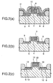
- Figs. 1A to 1C and Figs. 2A to 2C are sectional views showing a self-aligned silicide forming method of the present invention in the order of manufacturing steps.
- a MOS transistor For the formation of a MOS transistor, almost the same steps up to the step of forming a titanium film by sputtering as in the conventional method are carried out.
- a 300 nm-thick element-separating insulating film 2 is formed in a predetermined region on a P-conductive or P-well formed silicon substrate 1 by the known LOCOS process.
- boron impurity ions for the channel stopper are implanted and then, an about 8 nm-thick insulating film 3 is formed by thermal oxidation.
- An about 150 nm-thick polysilicon film is then formed over the entire surface by CVD (chemical vapor deposition) and an impurity such as phosphorus is doped.
- the polysilicon film is patterned to a desired shape by photolithography and dry etching to form a gate electrode 4.
- a silicon oxide film is formed over the entire surface by CVD and then anisotropic dry etching is carried out to form a sidewall spacer 5 on both side surfaces of the gate electrode 4.
- impurity ions such as arsenic, boron or the like are implanted to form the diffusion layer 106 by heating at 800 to 1,000°C.
- impurity ions such as arsenic, boron or the like are implanted to form the diffusion layer 106 by heating at 800 to 1,000°C.
- a diffusion layer including arsenic is formed and when the MOS transistor is of a P-channel type, a diffusion layer including boron is formed.
- the diffusion layer serves as source and drain regions of a transistor.
- an about 20 nm-thick titanium layer 8 is then formed over the entire surface by metal sputtering.
- a first heat treatment is carried out in an atmosphere of a hydrogen gas for 30 seconds.
- This first heat treatment is carried out in a lamp annealing device and the temperature thereof is set to 550°C, for example.
- the titanium film 7 is converted into a titanium layer containing hydrogen atoms, i.e., a hydrogen-containing titanium film 7'.
- a 10 to 20 nm-thick amorphous titanium silicide layer 8 (TiSix: x ⁇ 2) is formed only on the surface where the gate electrode 4 is exposed and the surface of the diffusion layer 6. However, since the heating temperature is sufficiently low, the silicide layer does not overgrow on the sidewall spacers or the element-separating insulating film 2.
- a second heat treatment is carried out in a nitrogen atmosphere for 30 seconds.
- This second heat treatment is carried out in the lamp annealing device and the temperature thereof is set to about 700°C.
- a crystalline C49-structured silicide layer 9 having a high electrical resistivity a titanium layer having nitrogen atoms, i.e., nitrogen-containing titanium layer 10 and a titanium nitride layer 11 are formed on the surface at which the gate electrode 4 is exposed and the surface of the diffusion layer 6.
- the above nitrogen-containing titanium layer 10 and the titanium nitride layer 11 are formed on the element-separating insulating film 2 and the sidewall spacers 5.
- the film thickness of the above C49-structured silicide layer 9 formed on the surface at which the gate electrode 4 is exposed and the surface of the diffusion layer 6 is larger than the film thickness of a silicide layer formed from a titanium layer having the same thickness by the prior art. This is because, only the silicification reaction which is in a trade-off relationship with the nitriding reaction is initiated in the first heat treatment in the hydrogen atmosphere. And in the subsequent second heat treatment in a nitrogen atmosphere the silicification reaction is promoted since the rate of the nitridation reaction of hydrogen-containing titanium is lower than that of titanium containing no hydrogen as will be described later.
- the nitrogen-containing titanium layer 10 and the titanium nitride layer 11 are removed by a chemical solution prepared by mixing an ammonia aqueous solution, purified water and a hydrogen peroxide solution.
- the nitrogen-containing titanium film is dissolved in the chemical solution but the titanium nitride layer does not.
- the titanium nitride film 11 is removed by lift-off caused by the dissolution of the underlying nitrogen-containing titanium layer 10.
- a chemical solution prepared by mixing sulfuric acid, purified water and a hydrogen peroxide solution may be used in place of the above chemical solution.
- the C49-structured silicide layer 9 is formed in a self-aligned manner only on the diffusion layer 6 for forming source and drain regions and the gate electrode 4.
- a heat treatment is then carried out in a nitrogen atmosphere for 60 seconds.
- the above lamp annealing device is used as the heat treatment device and the treatment temperature is set to 850°C, for example.
- the above C49-structured silicide layer 9 is converted into a C54-structured silicide layer 12 having a low electrical resistivity.
- a MOS transistor having a silicide layer selectively formed on the surface of the gate electrode 4 and the surface of the diffusion layer 6 is formed. And the electrical resistances of the gate electrode and the source drain regions are reduced.
- Fig. 3 shows the temperature-time profile of the heat treatment step to be carried out by the present invention.
- the semiconductor substrate in which the titanium layer is formed over the entire surface of semiconductor elements shown in Fig. 1B is inserted into the treatment chamber of the lamp annealing device, the atmosphere of the treatment chamber is fully substituted with a hydrogen gas, and lamp heating is carried out at a semiconductor substrate temperature of about 550°C for 30 seconds as the first heat treatment.
- heating is temporarily stopped, the atmosphere is substituted with a nitrogen gas, and lamp heating is carried out at a semiconductor substrate temperature of about 700°C for 30 seconds as the second heat treatment.
- the first heat treatment and the second heat treatment are carried out continuously without taking out the semiconductor substrate from the treatment chamber of the lamp annealing device between the first heat treatment and the second heat treatment. After the semiconductor substrate temperature is substantially lowered, the semiconductor substrate is taken out from the lamp annealing device to complete a series of heat treatment steps.
- the titanium film 7 is converted into a titanium layer containing hydrogen atoms, i.e., an amorphous titanium silicide layer 8 and a hydrogen-containing titanium film 7' on the ouuter surface is formed on the surface at which the gate electrode 4 is exposed and the surface of the diffusion layer 6.
- a hydrogen-containing titanium film 7' on the ouuter surface is formed on the surface at which the gate electrode 4 is exposed and the surface of the diffusion layer 6.
- a crystalline C49-structured silicide layer 9 having a high electrical resistivity, a titanium layer containing nitrogen atoms, i.e., nitrogen-containing titanium layer 10 and a titanium nitride layer 11 are formed on the surface at which the gate electrode 4 is exposed and the surface of the diffusion layer 6.
- the above nitrogen-containing titanium layer 10 and the titanium nitride layer 11 are formed on the element-separating insulating film 2 which is a silicon oxide film and the sidewall spacers 5.
- the film thickness of the C49-structured silicide layer 9 which is formed on the surface from which the gate electrode 4 is exposed and the surface of the diffusion layer 6 is larger than the film thickness of a silicide layer formed from a titanium film having the same thickness by the conventional method.
- the temperature of the first heat treatment may be higher than the temperature of the second heat treatment if the amorphous silicide layer, which of course is not limited to amorphous state, formed by the first heat treatment does not overgrow and the C49-structured silicide layer is formed by the second heat treatment.
- the first heat treatment may be carried out at 670°C for 1 second and the second heat treatment may be carried out at 650°C for 100 seconds.
- the risk of overgrowth caused by variations in processing conditions reduces and the throughput per unit time can be increased at the same time.
- the first reason is that a silicification reaction itself is promoted.
- a silicification reaction proceeds by the first heat treatment in a hydrogen atmosphere without causing a nitriding reaction. It was found that this silicification reaction is promoted by the effect of hydrogen.
- the amorphous titanium silicide layer 8 formed by this silicification reaction is neither C49-structured nor C54-structured silicide layer (both having a composition of TiSi2) and cannot function as a low-resistance wiring material by itself, it is easily changed into a C49-structured silicide layer. Further, the formation of the C49-structured silicide layer which proceeds by the diffusion of silicon atoms into the hydrogen-containing titanium layer is promoted by the subsequent second heat treatment in a nitrogen atmosphere at the same time.
- a C49-structured silicide layer formed by the present invention is thicker than a C49-structured silicide layer formed by the conventional method.
- Fig. 4 shows the dependence of the thickness of the titanium nitride film formed by the second heat treatment in a nitrogen atmosphere on the temperature of the first heat treatment in a hydrogen atmosphere.
- the nitridiation reaction of the hydrogen-containing titanium layer is suppressed more than in a normal titanium nitridation reaction. It can be seen that the suppression effect is larger as the temperature of the first heat treatment in a hydrogen atmosphere increases.
- a silicification reaction which proceeds with the diffusion of silicon atoms into titanium -this proceeds from the interface between titanium and silicon toward the surface of the film; and a nitriding reaction which proceeds with the diffusion of nitrogen atoms into titanium -this proceeds from the surface of the film in the direction of the substrate; compete with each other and have a trade-off relationship.
- the nitriding reaction (the formation of the titanium nitride layer and the nitrogen-containing titanium layer) and the silicification reaction (the formation of the silicide layer) struggle for a limited number of titanium atoms. Since the nitriding reaction is suppressed in the present invention, the silicification reaction which is in competition with the nitriding reaction is promoted.
- Fig. 5 shows the dependence of the resistance of the silicide layer on the line width of the gate electrode.
- the titanium film which is used for the formation of the silicide layer and formed by sputtering is 20 nm thick.
- the temperature of the first heat treatment which is carried out in a hydrogen atmosphere is 550°C and other steps are the same as in the above embodiment.
- the resistance value of the silicide layer formed by the conventional method is shown for comparison.
- the line width of the gate electrode is 0.1 to 0.6 ⁇ m, the resistance of the layer is almost uniform at 5 to 8 ⁇ in the present invention.
- the line width of the gate electrode is 0.3 ⁇ m or less
- the resistance of the layer sharply increases in the conventional method.
- the effect of the present invention becomes more marked as the design rule of semiconductor elements reduces or the integration of a semiconductor device increases.
- This effect is marked when the titanium film formed by sputtering is as thin as 30 nm or less, that is, the formation of the titanium nitride layer and the nitrogen-containing titanium layer which proceeds from the surface of titanium reaches the titanium silicide layer before the formation of the titanium silicide layer is completed. It has been described that when the line width of the gate electrode is as small as 0.3 ⁇ m or less, the silicification reaction slows down. The effect of the present invention is also marked when the silicification reaction slows down because of the concentration of impurities contained in polycrystal silicon as the gate electrode and the diffusion layer being high.
- FIG. 6 A second embodiment of the present invention will be explained with reference to Fig. 6.
- the second heat treatment in an atmosphere containing nitrogen atoms may be carried out subsequent to the first heat treatment in an atmosphere containing hydrogen atoms by switching the flow of gas and elevating the temperature after the first heat treatment without stopping heating.
- the throughput per unit time can be made greater than the process in which heating is temporarily stopped in the first embodiment as shown in Fig. 3.
- the temperature of the semiconductor substrate may be increased to a desired temperature, for example, 600°C in an atmosphere containing hydrogen atoms, then to a predetermined temperature, for example, 700°C, in an atmosphere containing nitrogen atoms, maintained at that temperature for a predetermined time, for example, 30 seconds, and then reduced.
- a predetermined temperature for example, 700°C
- the throughput per unit time can be made greater than the process in which heating is temporarily stopped in the above embodiment as shown in Fig. 3 and the process in which the temperature is elevated stepwise as shown in Fig. 6.
- One way to accomplish such a temperature-time profile is to place the substrate in a heat treatment chamber and change the gas type from hydrogen to nitrogen while raising the temperature.
- transfering the substrate from a hydrogen filled chamber to a nitrogen filled chamber, wherein both chambers have a predetermined temperature profile to meet the necessary process conditions should also be possible.
- the semiconductor substrate may be heated at a desired temperature for a desired time, for example, at 700°C for 30 seconds in an atmosphere containing both hydrogen atoms and nitrogen atoms.
- the promotion of the silicification reaction and the suppression of the nitriding reaction can be realized as in each of the above embodiments by setting the flow rate of a hydrogen gas to 10 times or more that of a nitrogen gas.
- the throughput per unit time can be increased and the substitution of a gas as in each of the above embodiments is unnecessary at the same time, thereby improving production stability.
- the first heat treatment which is carried out in an atmosphere containing hydrogen atoms and the second heat treatment which is carried out in an atmosphere containing nitrogen atoms are continuously performed after the formation of the titanium film over the entire surface of the semiconductor substrate by metal sputtering.
- the semiconductor substrate may be taken out from the treatment chamber of the lamp annealing device between the first and second heat treatments and exposed to the air.
- the first heat treatment and the second heat treatment may be carried out in separate lamp annealing devices as a matter of course.
- the throughput per unit time can be increased by carrying out the first heat treatment and the second heat treatment continuously in the same device.
- the present invention may be applied to the formation of a silicide layer on a polycrystal silicon film which is used as a wiring material between MOS transistors and a diffusion layer in a semiconductor device.
- the present invention may also be applied to the formation of a silicide layer on the surface of the diffusion layer which is exposed by opening contact holes in an interlayer insulating film to make conductive the diffusion layer on the surface of a substrate with a metal wiring and a metal plug on an interlayer insulating film.
- titanium has been described as an example of the refractory metal
- the present invention can be applied to any refractory metal or high melting point metal such as nickel, tantalum or zirconium if it forms a metal hydride.
- use of titanium is the most effective in reducing the resistivity of the silicide layer.
- the present invention comprises the first heat treatment step which is carried out in an atmosphere containing hydrogen atoms and the second heat treatment step which is carried out in an atmosphere containing nitrogen atoms for the formation of a refractory metal silicide layer by heating a refractory metal formed on the semiconductor substrate as heat treatment steps, the silicification reaction of the refractory metal is promoted by the effect of hydrogen and the nitriding reaction of the refractory metal containing hydrogen is suppressed. As a result, the silicification reaction is promoted and the formed silicide layer is made thick, thereby making it possible to manufacture a semiconductor device capable of reducing the resistance of wiring and increasing circuit operation speed in spite of a reduction in wiring width. Therefore, it is easy to form a silicide layer on a semiconductor device such as a MOS transistor having a reduced design rule, thereby further promoting an increase in the integration, density and speed of the semiconductor device.
Landscapes
- Electrodes Of Semiconductors (AREA)
- Internal Circuitry In Semiconductor Integrated Circuit Devices (AREA)
- Insulated Gate Type Field-Effect Transistor (AREA)
Applications Claiming Priority (2)
| Application Number | Priority Date | Filing Date | Title |
|---|---|---|---|
| JP97900/96 | 1996-04-19 | ||
| JP8097900A JP2882352B2 (ja) | 1996-04-19 | 1996-04-19 | 半導体装置の製造方法 |
Publications (2)
| Publication Number | Publication Date |
|---|---|
| EP0802563A2 true EP0802563A2 (de) | 1997-10-22 |
| EP0802563A3 EP0802563A3 (de) | 1998-09-02 |
Family
ID=14204621
Family Applications (1)
| Application Number | Title | Priority Date | Filing Date |
|---|---|---|---|
| EP97106310A Withdrawn EP0802563A3 (de) | 1996-04-19 | 1997-04-16 | Herstellungsverfahren für eine Halbleiteranordnung mit einer Metallsilizidschicht mit niedrigem Widerstand |
Country Status (4)
| Country | Link |
|---|---|
| EP (1) | EP0802563A3 (de) |
| JP (1) | JP2882352B2 (de) |
| KR (1) | KR970072211A (de) |
| TW (1) | TW326098B (de) |
Cited By (1)
| Publication number | Priority date | Publication date | Assignee | Title |
|---|---|---|---|---|
| WO2000026952A1 (en) * | 1998-10-29 | 2000-05-11 | Applied Materials, Inc. | Method for in-situ, post deposition surface passivation of a chemical vapor deposited film |
Families Citing this family (2)
| Publication number | Priority date | Publication date | Assignee | Title |
|---|---|---|---|---|
| KR20030002867A (ko) * | 2001-06-30 | 2003-01-09 | 주식회사 하이닉스반도체 | 반도체 소자의 제조 방법 |
| KR100400785B1 (ko) * | 2001-12-28 | 2003-10-08 | 주식회사 하이닉스반도체 | 반도체 소자의 살리사이드 형성 방법 |
Family Cites Families (6)
| Publication number | Priority date | Publication date | Assignee | Title |
|---|---|---|---|---|
| JPS57207372A (en) * | 1981-06-15 | 1982-12-20 | Nec Corp | Manufacture of metal oxide semiconductor integrated circuit device |
| JPS59123228A (ja) * | 1982-12-28 | 1984-07-17 | Nec Corp | 半導体装置の製造方法 |
| US5043790A (en) * | 1990-04-05 | 1991-08-27 | Ramtron Corporation | Sealed self aligned contacts using two nitrides process |
| US5190893A (en) * | 1991-04-01 | 1993-03-02 | Motorola Inc. | Process for fabricating a local interconnect structure in a semiconductor device |
| DE4402070C2 (de) * | 1994-01-25 | 1997-10-16 | Gold Star Electronics | Verfahren zum Herstellen eines aus PtSi-Platinsilizid bestehenden Kontaktstopfens |
| US5789318A (en) * | 1996-02-23 | 1998-08-04 | Varian Associates, Inc. | Use of titanium hydride in integrated circuit fabrication |
-
1996
- 1996-04-19 JP JP8097900A patent/JP2882352B2/ja not_active Expired - Lifetime
-
1997
- 1997-04-16 EP EP97106310A patent/EP0802563A3/de not_active Withdrawn
- 1997-04-17 TW TW086105014A patent/TW326098B/zh active
- 1997-04-18 KR KR1019970014893A patent/KR970072211A/ko not_active Ceased
Cited By (3)
| Publication number | Priority date | Publication date | Assignee | Title |
|---|---|---|---|---|
| US6432479B2 (en) | 1997-12-02 | 2002-08-13 | Applied Materials, Inc. | Method for in-situ, post deposition surface passivation of a chemical vapor deposited film |
| WO2000026952A1 (en) * | 1998-10-29 | 2000-05-11 | Applied Materials, Inc. | Method for in-situ, post deposition surface passivation of a chemical vapor deposited film |
| KR100798552B1 (ko) * | 1998-10-29 | 2008-01-28 | 어플라이드 머티어리얼스, 인코포레이티드 | 화학 기상 증착된 필름의 인-시츄 후증착 표면 부동태화 방법 |
Also Published As
| Publication number | Publication date |
|---|---|
| KR970072211A (ko) | 1997-11-07 |
| JPH09283466A (ja) | 1997-10-31 |
| EP0802563A3 (de) | 1998-09-02 |
| JP2882352B2 (ja) | 1999-04-12 |
| TW326098B (en) | 1998-02-01 |
Similar Documents
| Publication | Publication Date | Title |
|---|---|---|
| JP2857006B2 (ja) | Mos集積回路上の自己整列珪化コバルト | |
| KR100440840B1 (ko) | 반도체 장치의 제조 방법 및 반도체 장치 | |
| JP2692617B2 (ja) | 半導体装置の製造方法 | |
| KR0183490B1 (ko) | 반도체 소자의 제조 방법 | |
| EP0603360A1 (de) | Verfahren zur herstellung einer lokalen verbindung und eines hohen polisiliziumwiderstands | |
| JPH0864551A (ja) | 導体および半導体装置の製造方法 | |
| JP2751859B2 (ja) | 半導体装置の製造方法 | |
| JP2001077050A (ja) | 半導体装置の製造方法 | |
| US5877085A (en) | Method of manufacturing semiconductor device | |
| JP2930042B2 (ja) | 半導体装置の製造方法 | |
| EP0802563A2 (de) | Herstellungsverfahren für eine Halbleiteranordnung mit einer Metallsilizidschicht mit niedrigem Widerstand | |
| JP3033526B2 (ja) | 半導体装置の製造方法 | |
| JP3376158B2 (ja) | 半導体装置の製造方法 | |
| JPH03288443A (ja) | 半導体装置の製造方法 | |
| US7320938B2 (en) | Method for reducing dendrite formation in nickel silicon salicide processes | |
| JPH069213B2 (ja) | 半導体装置の製造方法 | |
| JPH1140679A (ja) | 半導体装置およびその製造方法 | |
| JP2850883B2 (ja) | 半導体装置の製造方法 | |
| JPH11195619A (ja) | 半導体装置の製造方法 | |
| JP2900897B2 (ja) | 半導体装置の製造方法 | |
| JPH07201777A (ja) | 半導体装置の製造方法 | |
| JP3094914B2 (ja) | 半導体装置の製造方法 | |
| JP3258934B2 (ja) | セルフ・アライン・ケイ化物の改良された製造方法 | |
| JP2636787B2 (ja) | 半導体装置の製造方法 | |
| JPH0645279A (ja) | 半導体装置及びサリサイド構造の形成方法 |
Legal Events
| Date | Code | Title | Description |
|---|---|---|---|
| PUAI | Public reference made under article 153(3) epc to a published international application that has entered the european phase |
Free format text: ORIGINAL CODE: 0009012 |
|
| AK | Designated contracting states |
Kind code of ref document: A2 Designated state(s): DE FR GB IT NL SE |
|
| PUAL | Search report despatched |
Free format text: ORIGINAL CODE: 0009013 |
|
| AK | Designated contracting states |
Kind code of ref document: A3 Designated state(s): DE FR GB IT NL SE |
|
| 17P | Request for examination filed |
Effective date: 19980729 |
|
| STAA | Information on the status of an ep patent application or granted ep patent |
Free format text: STATUS: THE APPLICATION HAS BEEN WITHDRAWN |
|
| 18W | Application withdrawn |
Withdrawal date: 20020130 |