EP0783207B1 - Vorrichtung und Verfahren zur digitalen Signalverarbeitung - Google Patents
Vorrichtung und Verfahren zur digitalen Signalverarbeitung Download PDFInfo
- Publication number
- EP0783207B1 EP0783207B1 EP96309281A EP96309281A EP0783207B1 EP 0783207 B1 EP0783207 B1 EP 0783207B1 EP 96309281 A EP96309281 A EP 96309281A EP 96309281 A EP96309281 A EP 96309281A EP 0783207 B1 EP0783207 B1 EP 0783207B1
- Authority
- EP
- European Patent Office
- Prior art keywords
- sigma
- signal
- level
- amplitude
- delta
- Prior art date
- Legal status (The legal status is an assumption and is not a legal conclusion. Google has not performed a legal analysis and makes no representation as to the accuracy of the status listed.)
- Expired - Lifetime
Links
Images


Classifications
-
- H—ELECTRICITY
- H03—ELECTRONIC CIRCUITRY
- H03M—CODING; DECODING; CODE CONVERSION IN GENERAL
- H03M7/00—Conversion of a code where information is represented by a given sequence or number of digits to a code where the same, similar or subset of information is represented by a different sequence or number of digits
- H03M7/30—Compression; Expansion; Suppression of unnecessary data, e.g. redundancy reduction
- H03M7/3002—Conversion to or from differential modulation
- H03M7/3004—Digital delta-sigma modulation
- H03M7/3013—Non-linear modulators
Definitions
- This invention relates to a digital signal processing method and apparatus for switching between a sigma-delta modulation signal as an input signal produced by sigma-delta modulation, and sigma-delta re-modulated signal obtained on sigma-delta re-modulation of the input signal.
- a method of digitizing speech signals for recording, reproduction and transmission is implemented in a recording/reproducing apparatus for a disc-shaped recording medium, including an optical disc, such as a compact disc (CD), or a digital audio tape (DAT), or in digital broadcasting, such as satellite broadcasting.
- a digital audio transmission apparatus the format has conventionally been set for the sampling frequency of 48 kHz or 44.1 kHz and the number of quantization bits of 16 or 24 bits for digitization.
- the number of quantization bits of digital audio data prescribes the dynamic range of demodulated audio signals.
- the number of quantization bits needs to be expanded from 16 bits of the current system to 20 or 24 bits.
- the number of quantization bits can hardly be increased, so that it has been difficult to take out audio signals of higher quality from the conventional digital-audio transmission apparatus.
- Fig.1 shows, in a block diagram, a ⁇ modulation circuit for ⁇ modulation of, for example, 1-bit digital data.
- an input audio signal from an input terminal 181 is supplied via an adder 182 to an integrator 183.
- a signal from the integrator 183 is supplied to a comparator 184 where it is compared to, for example, a neutral point potential of the input audio signal for effecting one-bit quantization every sampling period.
- the frequency of the sampling period is 64 or 128 times 48 kHz to 44.1 kHz conventionally employed.
- the quantized data is supplied to a 1-sample delay unit 185 so as to be delayed one sampling period.
- This delayed data is converted by, for example, a one-bit D/A converter 186 into analog signals which are then is sent to an adder 182 so as to be added to the input audio signal from the input terminal 181.
- the comparator 184 outputs quantized data which is outputted at an output terminal 187.
- the ⁇ modulation circuit has a circuit structure that is suited to integration, and high precision in A/D conversion can be realized relatively easily, so that it has hitherto been used widely in an A/D converter.
- the ⁇ modulated signal can be restored to the analog audio signal by being passed through a simple analog low-pass filter.
- the ⁇ modulation circuit can be applied to a recorder handling high-quality data or to data transmission.
- fading operations there are a fade out operation of gradually lowering the reproduced signal level as time elapses, and a fade-in operation of gradually raising the audio signal level from a zero level.
- These fading operations are customary as signal processing in the direction of the amplitude of the audio signal.
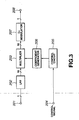
- the above fading operation carried ut on the above multi-bit digital audio transmission apparatus, is explained by referring to Fig.2 .
- the multibit digital audio signal such as 16-bit signal, from an input terminal 191
- a control signal designating the fading start timing or the fading speed is supplied to a control terminal 194
- this control signal is fed to a control circuit 195 for generating a desired fading signal.
- This fading signal is fed to a coefficient generator 196 for generating a coefficient which gradually lowers the audio signal level to zero. This coefficient is supplied to the multiplier 192.
- the digital speech signal supplied to the input terminal 191, has its signal level gradually lowered at a designated speed by a control signal as from the timing designated until it is muted to a zero level, so as to be outputted at the output terminal 193, by way of performing the fade-out operation.
- the fade-in operation of gradually raising the speech signal level from the zero level may also be effected by reversing the sequence of generation of the coefficients.
- the amplitude information is also represented as a 1-bit pattern on the time axis, such that it has been difficult to multiply the amplitude by the multiplier 192 and to perform amplitude processing on the 1-bit basis.
- ⁇ signal may be converted into signals of the CD or DAT format, using a low-pass filter, and to perform the above fading operation on the converted signal. That is, in Fig.3 , a 1-bit ⁇ signal, for example, is fed via an input terminal 201 to a low-pass filter 202 for conversion into, for example, 16-bit multi-bit speech signal. This converted digital speech signal is sent to a multiplier 203.
- a control signal designating the fading starting timing or fading speed is fed to a control input terminal 204 and thence supplied to a control circuit 205 for generating a desired fading signal.
- this fading signal supplied to a coefficient generator 206 there is generated a coefficient gradually lowering the speech signal level to zero. This coefficient is sent to the multiplier 203.
- the multi-bit digital audio signal from the low-pass filter 202 is taken out at the multiplier 203.
- This digital audio signal is further sent to a ⁇ modulator 207 for re-conversion into, for example, a 1-bit ⁇ signal which is outputted at an output terminal 208.
- the ⁇ signal from the input terminal 201 is outputted at the output terminal 208 by way of performing the fade-out operation.
- the fade-in operation of gradually raising the speech signal level from the zero level may also be performed by reversing the sequence of coefficient generation.
- the ⁇ signal supplied to the input terminal 201, is converted at all times into, for example, a 16-bit multi-bit digital speech signal by the low-pass filter 202. That is, with the above device, the ⁇ signal is passed through the low-pass filter 202 and the ⁇ modulator 207 even if the signal has not been processed with fading.
- the signal characteristics become the same as those with the conventional CD or DAT, such that it becomes impossible to exploit characteristics proper to ⁇ modulation, such as broad band and high dynamic range.
- Considerations of digital circuit complexity has lead to work on ⁇ based filteringand thus digitally processing the audio in formation in the ⁇ bit stream directly ( Kershaw S.M. Sandler M.B. "Digital Signal Processing on a Sigma-Delta Bit stream"; IEE Colloquium on Oversampling Techniques and Sigma-Delta Modulation 30.3.1994 ).
- the fading operation can be done by directly supplying the ⁇ signal supplied to the input terminal 201 to the ⁇ modulator 207, without passing the ⁇ signal through the low-pass filter 202.
- the signal is passed through the ⁇ A modulator 207 if it is not processed with fading, such that it becomes similarly impossible to exploit characteristics proper to ⁇ modulation, such as broad band and high dynamic range.
- the above two ⁇ signals, switched by the switch 217 are signals modulated on the time axis by different ⁇ modulators, even although the two signals have substantially the same analog audio signal components, so that, if the signals are switched directly, significant noise is generated at the switching point, thus rendering the device practically unusable.
- the present invention provides a digital signal processing apparatus according to claim 1.
- This arrangement realizes switching in a manner free from noise.
- the signal-delta modulation means sets the first stage feedback loop/second stage feedback loop gain ratio to an integer value.
- the input signal delaying means determines the pre-set number of samples based on the above gain ratio.
- the digital signal processing device also includes pattern coincidence detection means for detection of coincidence of the delayed sigma-delta modulated signal and the sigma-delta re-modulated signal over a plurality of samples.
- the switching control means controls the switching means based on the result of detection obtained by the pattern coincidence detection means. This realizes switching with more reliable noise suppression.
- the digital signal processing device sets the initial value of the integrator of the signal-delta modulation means to zero by the switching control means immediately before input of the input signal and/or during the time the delay signals from the first and second input signal delaying meas are selected by switching. This realizes switching with still more reliable noise suppression.
- the digital signal processing device also includes amplitude controlling means for controlling the amplitude level of a level adjusted signal having the amplitude level adjusted by he level adjustment means.
- the switching control means causes the amplitude control means to control the amplitude level of the level-adjusted signal after causing the switching means to switch from the delayed sigma-delta modulated signal from the input signal delaying means to the sigma-delta re-modulated signal obtained on sigma-delta modulation of the level adjusted signal.
- the digital signal processing device also includes amplitude controlling means for controlling the amplitude level of the level adjusted signal having its amplitude level adjusted by the level adjustment means, level difference detection means for detecting the difference between the maximum amplitude level of the level-adjusted signal and the amplitude level of the output following amplitude control during the time the amplitude controlling means is controlling the amplitude level of the level-adjusted signal, cumulative addition means for cumulatively adding the level difference from the level difference detection means with a maximum amplitude level width length equal to twice the maximum amplitude level of the level-adjusted signal, and subtraction control means for gradually subtracting the cumulative sum of the cumulative addition means from the maximum amplitude level of the level adjusted signal after the amplitude control in the amplitude controlling means.
- the switching control means causes the switching means to switch from the sigma-delta modulated signal to the delayed sigma-delta modulated signal after the end of subtraction of the cumulative sum in the subtraction control means.
- the digital signal processing device of the present invention also includes error detection means for detecting an uncorrectable burst error in the sigma-delta modulated signal, delaying means provided downstream of he error detection means for delaying the sigma-delta modulated signal, fade-out means for fading out the sigma-delta modulated signal via the delay means, fade-in means for fading in the sigma-delta modulated signal via the delay means, and control means for causing the fade-out means to fade out the sigma-delta modulated signal delayed by the delaying means up to directly before an uncorrectable burst error immediately to a zero level if the detection means detects such uncorrectable burst error in the sigma-delta modulated signal.
- the control means causes the fade-in means to fade in the sigma-delta modulated signal directly after the burst error up to the maximum amplitude level. This arrangement realizes muting processing in which the signal level on occurrence of burst error may be reduced to zero for noise suppression.
- the sigma-delta modulation processing means of the digital signal processing device includes plural stages of serially connected integrators and a local feedback loop for feeding back outputs of the plural stages of the integrators to inputs of preceding stage integrators. This renders it possible to reduce noise components to assure a broad dynamic range in an audible band.
- the present invention also includes a digital signal processing device according to claim 12.
- This arrangement enables the sound cross-faded from the original audio signal of the first channel to the original audio signal of the second channel to be produced under effective noise suppression.
- the sigma-delta modulation processing means sets the first stage feedback loop/second stage feedback loop gain ratio to an integer.
- the input signal delaying means determines the pre-set number of the samples based on the above gain ratio.
- the digital signal processing device also includes pattern coincidence detection means for detecting the coincidence of the first delayed sigma-delta modulated signal and the sigma-delta re-modulated signal over a plurality of samples and for detecting the coincidence of the second delayed sigma-delta modulated signal and the sigma-delta re-modulated signal over a plurality of samples.
- the first delayed sigma-delta modulated signal is switched to the sigma-delta re-modulated signal or vice versa based on a control signal obtained by the pattern coincidence detection means, while the second delayed sigma-delta modulated signal is switched to the sigma-delta re-modulated signal or vice versa based on the control signal obtained by the pattern coincidence detection means.
- the digital signal processing device causes the switching control means to set the initial value of the integrator of the sigma-delta modulation processing means to zero directly before input of the input signal and/or during the time the delayed signal from the first and second input signal delaying means is selected by switching by the switching means.
- the sigma-delta modulation processing means of the digital signal processing device includes plural stages of serially connected integrators and a local feedback loop for feeding back outputs of the plural stages of the integrators to inputs of preceding stage integrators.
- the amplitude control output adjustment means of the digital signal processing device also includes subtraction means for subtracting a pre-set value from an output signal obtained by the first and second amplitude control means.
- the limiting value of the limiter means is set to an integer number times the maximum amplitude level width.
- Muting pattern signal generating means is provided in one of the above-mentioned two channels.
- switching between a delayed sigma-delta modulated signal obtained on delaying a sigma-delta modulated signal as an input signal obtained on sigma-delta modulation processing and a sigma-delta re-modulated signal obtained on second sigma-delta conversion processing on the input signal is done by a switching step. This realizes switching in a manner free from noise generation.
- the digital signal processing method includes an amplitude controlling step of controlling the amplitude level of the level-adjusted signal having its amplitude level adjusted by the level adjustment step.
- the switching control step causes the switching step to switch the sigma-delta modulated signal from the input signal delaying step to the sigma-delta re-modulated signal obtained on sigma-delta modulation of the level-adjusted signal.
- the switching control step then causes the amplitude control step to control the amplitude of the level-adjusted signal. This realized switching between the amplitude-controlled sigma-delta signal and the original 1-bit signal free from deterioration in the sound quality in through-time.
- the digital signal processing method first causes the switching control step to switch from the first delayed input signal to the sigma-delta re-modulated signal and then controls the operation of the first and second amplitude control steps for effecting cross-fading amplitude-control of the sigma-delta modulated signal and the other sigma-delta modulated signal, thus realizing cross-fading with minimum sound quality deterioration and suppression of the switching noise.
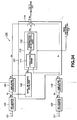
- the present first embodiment is directed to a digital signal processing device 1 configured for switching between a ⁇ modulated signal S A , as an input signal obtained on sigma-delta ( ⁇ ) modulation, and a ⁇ re-modulated signal S B , obtained on ⁇ re-modulation on the input signal, by a changeover switch 4, as shown in Fig.5 .
- the digital signal processing device 1 includes a delay line 3 for delaying the original ⁇ modulated signal from the input terminal 2 a pre-set number of samples, and a ⁇ modulator 6 having five integrators and configured for outputting the above ⁇ re-modulated signal with the gain ratio between the gain of the initial stage feedback loop and the gain of the next stage feedback loop set to 16.
- the digital signal processing device 1 also includes a bit length converter 5 for matching the amplitude level of the original ⁇ modulated signal entering the ⁇ modulator 6 to that of the feedback signal to the initial stage integrator employed in the ⁇ modulator 6.
- the switching operation of the changeover switch 4 is controlled depending on a changeover control signal SE supplied from a control signal input terminal 7 for outputting the original ⁇ modulated signal delayed a pre-set number of samples by the delay line 3 (original 1-bit delay signal) S A or the ⁇ re-modulated signal ( ⁇ re-modulated 1-bit signal) S B .
- the ⁇ modulator 6 is configured as a five-order (five-stage) ⁇ modulator made up of five integrators.
- a first integrator 11 is configured for shifting an addition output of an adder 61 by a shifter 62 for returning the shifted output to the adder 61, as shown in Fig.6 .
- the remaining integrators are configured in a similar manner.
- the 16-bit signal having its amplitude level maximized to the maximum amplitude level by adjustment in the bit length converter 5, is integrated by the first integrator 11 via an adder 10, as shown in Fig.7 , and is multiplied in a first coefficient multiplier 12 by a coefficient 1/16, so as to be then supplied to the second stage.
- An input signal to the second stage is integrated via an adder 13 by a second integrator 14 and multiplied by a second coefficient multiplier 15 with a coefficient 1/8 so as to be supplied to the third stage.
- An input signal to the third stage is integrated via an adder 16 of the third stage by a third integrator 17 and multiplied by a third coefficient multiplier 18 with a coefficient 1/4 so as to be supplied to the fourth stage.
- An input signal to the fourth stage is integrated via an adder 19 by a fourth integrator 20 and multiplied by ⁇ by a fourth coefficient multiplier 21 so as to be supplied to a fifth stage.
- An input to the fifth stage is integrated via an adder 22 by a fifth integrator 23 and quantized by a 1-bit quantizer 24 into a 1-bit signal which is supplied to the changeover switch 4.
- the 1-bit signal is also converted into a 16-bit signal by a bit length converter 25 so as to be fed back to the adders 10, 13, 16, 19 and 22.
- the gain ratio to the initial stage feedback loop exclusive of the integrator ahead and at back of the 1-bit quantizer 24 of the next-stage feedback loop is set to an integer value of 16, as will now be explained in detail.
- the delay line 3 sets the number of delayed samples to 16.
- the bit length converter 5 converts the original 1-bit signal into 16-bit multiple-bit data so that the amplitude level will be of the same level as the amplitude level of the 16-bit feedback signal fed back from the 1-bit quantizer 24 via the bit length converter 25 to the first integrator 11 as the first-stage integrator.
- the changeover switch 4 receives the ⁇ modulated 1-bit signal S B , obtained on ⁇ modulation by the ⁇ modulator 6, at a fixed terminal b, while receiving the original 1-bit signal S A , delayed by 16 samples by the delay line 3, at a fixed terminal a.
- the changeover switch 4 brings a movable contact c into contact with the fixed terminals a or b depending on the changeover control signal SE supplied from the control signal input terminal 7 for supplying the original 1-bit signal or the ⁇ modulated 1-bit signal S B .
- the five integrators used in the ⁇ modulator 6 may be configured as shown in Fig.9 .
- the first integrator 11 delays the addition output of an adder 63 by a shifter 64 as the addition output is fed back to the adder 63.
- the remaining integrators are configured in the similar manner.
- the ⁇ modulator 6 has its feedback loop structure modified from that shown in Fig.7 , as shown in Fig.10 . That is, a shifter 26 is provided ahead of the bit length converter 25.
- the 1-bit quantizer 24 quantizes the integration output of the fifth integrator 23 into 1-bit data.
- the 1-bit signal of the 1-bit quantizer 24 is supplied via shifter 26 to the bit length converter 25, while being supplied to the fixed terminal b of the changeover switch 4.
- the bit length converter 25 re-converts the delayed 1-bit signal into a 16-bit signal which is supplied to the adders 10, 13, 16, 19 and 22.
- the number of delays in terms of the input/output difference becomes smaller by one sample, so that the number of delay samples of the delay line 3 is equal to (gain ratio - 1), based on the integer gain ratio of the second stage feedback loop gain to the first stage feedback loop gain, ahead and at back of the 1 bit quantizer 24, excluding the integrator.
- the gain ratio of the second stage feedback loop gain to the first stage feedback loop gain in the ⁇ modulator 6 is set to an integer, while the number of delay samples of the delay line 3, is determined on the basis of the gain ratio.
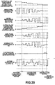
- the noise generated at a switching point as shown in Fig.llA in case an output of the conventional digital signal processing device, such as the device configured as shown in Fig.1 , is converted into an analog audio signal, may be suppressed, as shown in Fig.11B .
- a second embodiment is now explained by referring to Figs.12 and 13 .
- the second embodiment is directed to a digital signal processing device 27 configured for switching between the ⁇ modulated signal S A , as an input signal obtained on ⁇ modulation, and a re-modulated signal S B , obtained on ⁇ remodulation of the input signal.
- the digital signal processing device 27, however, is designed for detecting coincidence between the ⁇ modulated signal S A and the ⁇ re-modulated signal S B over plural samples and switches between the ⁇ modulated signal S A and ⁇ re-modulated signal SB responsive to the pattern coincidence detection signal.
- the digital signal processing device 27 corresponds to the digital signal processing device 1 of the first embodiment shown in Fig.5 to which are added a pattern coincidence detector 28 and a switching controller 29.
- the present second embodiment is otherwise the same as the first embodiment so that the corresponding parts are depicted by the same numerals and the corresponding description is not made.
- the ⁇ modulator 6 may be configured as shown in Fig.7 as a five-order ⁇ re-modulator employing five integrators shown in Fig.6 , or may also be configured as shown in Fig.10 as a five-order ⁇ re-modulator employing five integrators shown in Fig.7 .
- the pattern coincidence detector 28 monitors the original 1-bit delayed signal S A from the delay line 3 and the ⁇ re-modulated signal S B from the ⁇ modulator 6 and, on detection of pattern coincidence continuing over, for example, four samples, generates a pattern coincidence detection signal S T which is sent to the switching controller 29.
- the switching controller 29 controls the switching of the changeover switch 4 in order to output the original 1-bit delayed signal S A or the ⁇ re-modulated 1-bit signal S B at the changeover switch 4.
- Fig.13 illustrates, in a timing chart, the operation of the digital signal processing device 27.
- the switching controller 29 Directly after inversion from the side S A to the side S B of a changeover control signal S D supplied from the control-signal input terminal 7, the switching controller 29 generates a switch changeover signal SE from the fixed terminal a to the fixed terminal b, at the next sampling timing t0 of reception of the pattern coincidence detection signal S T supplied from the pattern coincidence detector 28, and sets the movable contact piece c of the changeover switch 4 from its fixed terminal a to its fixed terminal b.
- the digital signal processing device 27 then sums a signal S M of the four sample pattern coincident portion to the original 1-bit delay signal S A for a period La and further sums the ⁇ re-modulated 1-bit signal S B to the resulting signal to produce a 1-bit signal output S F which is outputted at the output terminal 8.
- the present digital signal processing device 27 first controls the changeover timing by pattern coincidence detection by the pattern coincidence detector 28 and subsequently switches between the original 1-bit delay signal S A and the ⁇ re-modulated 1-bit signal S B , so that switching can be done under more reliable noise suppression.
- the present third embodiment is directed to a digital signal processing device 30 which, when switching between the original 1-bit delayed signal S A and the ⁇ re-modulated 1-bit signal S B , detects coincidence between these signals S A and S B over plural samples and switches between the signals S A and SB responsive to the pattern coincidence detection signal.
- the initial value of the integrator in the ⁇ modulator is cleared to zero directly before inputting of the ⁇ modulated signal to the input terminal 2 and/or during the time of selection by the changeover switch 4 of the original 1-bit delay signal S A from the 16-tap delay line 3.
- a ⁇ modulator 31 corresponds to the ⁇ modulator 6 of the digital signal processing device 27 of the second embodiment of Fig.12 to which has been added an integrator 0-clear controller designed for clearing the initial value of the integrator to 0 by a ⁇ modulator integrator clear signal S G supplied from a switching controller 32.
- the present digital signal processing device is otherwise the same as the second embodiment so that equivalent parts are denoted by the same numerals and the corresponding description is not made.
- the ⁇ modulator 31 may be configured as a five-order ⁇ modulator employing five integrators shown in Fig.6 , as shown in Fig.7 , or may also be configured as a five-order ⁇ modulator employing five integrators shown in Fig.9 , as shown in Fig.10 .
- Fig.15 shows, by a timing chart, the operation of the present digital signal processing device 30.
- the pattern coincidence detector 28 monitors the original 1-bit delay signal S A from the delay line 3 and the ⁇ re-modulated 1-bit signal S B from the ⁇ modulator 6, every sampling period, and generates a pattern coincidence detection signal S T if 1-bit data coincide for four samples on end.
- four patterns coincide at three pattern coincident portions SM1, SM2 and SM3.
- the switching controller 32 Inverts the switch changeover signal SE to the fixed terminal a or to the fixed terminal b at the sampling timings t1, t2 and t3 next to the reception of the pattern coincidence detection signal S T supplied from the pattern coincidence detector 28. Also, during the time the delayed original 1-bit signal S A is selected by the changeover switch 4, the switching controller 32 sends the ⁇ re-modulator integrator clear signal S G to the ⁇ modulator 31. Thus the integrated value accumulated in the integrator in the ⁇ modulator 31 is cleared to zero before an output of the bit length converter 5 is supplied to the ⁇ modulator 31.
- the digital signal processing device 30 then connects the original 1-bit delay signal S A over a period L a1 to the ⁇ modulated 1-bit signal S B over a period L b1 with tie interposition of the pattern coincident portion S M1 and further connected to the resulting signal the original 1-bit delay signal S A over a period L a2 with the interposition of the four-pattern coincident portion S M2 to produce a 1-bit signal output S F which is outputted at the output terminal 8.
- the present fourth embodiment is directed to a digital signal processing device 34 switching between the delayed original 1-bit signal S A and the ⁇ re-modulated 1-bit signal S B obtained on clearing the integrated value in the integrator in the ⁇ modulator 31 as described above to zero, after detection of coincidence of several patterns on end by pattern coincidence detection, as shown in Fig.16 .
- the digital signal processing device 34 converts the ⁇ re-modulated 1-bit signal S B into a signal processed with fade-out which is a sort of amplitude control processing.
- the amplitude control processing is such signal processing in which signal processing is done in the amplitude direction, such as fade-out in which the reproduced audio signal level is gradually lowered with time, fade-in in which the audio signal level is gradually raised from the zero level, or cross-fade.
- a digital signal processing device 34 as a fourth embodiment, is provided with an amplitude controller 35 between the ⁇ modulator 31 and the bit length converter 5 of the digital signal processing device 30 of the third embodiment.
- the amplitude controller 35 is controlled by a switching controller 38.
- the amplitude controller 35 performs amplitude control processing, such as fade-out described above, on a bit-length-converted signal S I , as a level-adjusted signal outputted by the bit length converter 5.
- the switching controller 38 causes the changeover switch 4 to perform switching from the original 1-bit delay signal S A to the ⁇ re-modulated 1-bit signal S B obtained on ⁇ re-modulation of the bit-length-converted signal S I by the ⁇ modulator 31.
- the amplitude level of the bit-length-converted signal S I at this time is of the maximum amplitude level.
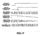
- Fig.17 illiterates, by a timing chart, the operation of the present digital signal processing device 34.
- the switching controller 38 sends a switching control signal S E to the changeover switch 4 after waiting for supply of the four-pattern coincidence detection signal S T from the pattern coincidence detector 28.
- the movable contact c of the changeover switch 4 is changed over from the fixed terminal a to the fixed terminal b.
- the changeover switch 4 then switches, at a changeover timing t0, from the original 1-bit delay signal S A to the ⁇ re-modulated 1-bit signal S B obtained on directly ⁇ modulating the bit length conversion signal S I .
- the switching controller 38 sends the ⁇ re-modulator integrator clear signal S G to the ⁇ modulator 31.
- the switching controller 38 causes transition of a coefficient output SJ of a coefficient generator 36 of the amplitude controller 35 from 1 to 0.
- the amplitude controller 35 also includes a multiplier 37 and multiplies the bit-length-converted signal S I with the coefficient output SJ which undergoes transition from 1 to 0 on execution of the fade-out processing. The amplitude controller 35 then causes an amplitude controller output S K to undergo transition from the maximum amplitude level to the zero level.
- the ⁇ modulator 31 may be configured as a five-order ⁇ modulator employing five integrators shown in Fig.6 , as shown in Fig.7 , or may also be configured as a five-order ⁇ modulator employing five integrators shown in Fig.9 , as shown in Fig.10 .
- the ⁇ modulator 31 ⁇ re-modulates the amplitude controller output S K and outputs the ⁇ re-modulated 1-bit signal S B .
- a fade-out processed signal can be heard, in which the noise otherwise produced on switching from the analog audio signal to a zero-amplitude level is suppressed.
- the present fifth embodiment s directed to a digital signal processing device 41 switching between the delayed original 1-bit signal obtained on ⁇ modulation and the ⁇ re-modulated 1-bit signal S B obtained on clearing the integrated value in the integrator in the ⁇ modulator to zero after detection of coincidence of several patterns on end by pattern coincidence detection.
- the digital signal processing device 41 sets the ⁇ re-modulated 1-bit signal S B into a signal processed with fade-out/in processing and connects the signal SB to the original 1-bit delay signal S A .
- the fade-out/in precessing means such processing in which fade-in precessing is performed in succession to the fade-out processing.
- the present digital signal processing device 41 thus performs amplitude control processing in which the original 1-bit delay signal S A is, as it were, processed with fade-in and subsequently restored to the original level.
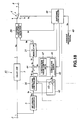
- the digital signal processing device 41 includes, in addition to the delay line 3, pattern coincidence detector 28, bit length converter 5, amplitude controller 35 and the ⁇ modulator 31, a level difference detector 42, a cumulative adder 46, a subtraction value control gate 47 and a switching controller 48, as shown in Fig.18 .
- the level difference detector 42 detects the difference between the maximum amplitude level of the bit length conversion output S I entering the ⁇ modulator 31 during the time the amplitude controller 35 is controlling the amplitude level 1 of the bit-length-converted output S I of the bit length converter 5 and the amplitude level of the amplitude-controlled output.
- the cumulative adder 46 cumulatively sums the level difference from the level difference detector 42 with the maximum amplitude level width length which is twice as large as the above-described maximum amplitude level.
- the subtraction value control gate 47 gradually subtracts the cumulative sum value of the cumulative adder 46 from the maximum amplitude level of the amplitude controller output S K entering the ⁇ modulator 31 after amplitude control by the amplitude controller 35 using an adder/subtractor 44.
- the switching controller 48 controls the operation of the amplitude controller 35 as will be explained subsequently.
- the switching controller causes the changeover switch 4 to switch the output of the ⁇ modulator 31 to the original 1-bit delay signal S A after pattern coincidence detection by the pattern coincidence detector 28 and to output the signal S A .
- the cumulative adder 46 and the subtraction value control gate 47 make up the subtraction value processing controller 45.
- the amplitude controller 35 has a configuration shown in Fig.16 , that is, includes the coefficient generator 36 and the multiplier 37.
- the coefficient generator 36 generates a coefficient output SJ undergoing transition from 1 t 0 and then from 0 to 1, in a manner of executing the fade-out/in processing, under control by the switching controller 48.
- the multiplier 37 multiplies the bit length conversion signal SL with the above coefficient output SJ.
- the level difference detector 42 is configured as shown in Fig.16 , that is, the detector 42 detects the difference between the maximum amplitude level of the bit-length-converted output S I entering the ⁇ modulator 31 during the time the amplitude controller 35 is controlling the amplitude level of the bit length conversion output S I of the bit length converter 5 and the output S K of the amplitude controller 35 and sends the level difference detection output SL to the cumulative adder 46 in the subtraction value processing controller 45.
- Fig.19 is an output signal waveform diagram for illustrating the operation of the level difference detector 42 and the subtraction value processing controller 45.
- Fig.20 is a timing chart for illustrating the fade-out/in processing performed by the digital signal processing device 41.
- the switching controller 48 When the fade-out/in processing signal S H is supplied from a control signal input terminal 49 to the switching controller 48, the switching controller 48 first awaits the oncoming of the 4-pattern coincidence detection signal S T for the pattern coincidence detection circuit 28, and subsequently routes a switch changeover signal S E to the changeover switch 4. The switching controller 48 then causes the movable contact c of the changeover switch 4 to be changed over from the fixed terminal a to the fixed terminal b. Then, at a switching timing t0, the changeover switch 4 switches the bit length conversion signal S I from the original 1-bit delayed signal S A to the ⁇ re-modulated 1-bit signal S B .
- the changeover switch 4 is supplying the ⁇ re-modulator integrator clear signal S G to the ⁇ modulator 31.
- the switching controller 48 causes transition of the coefficient output SJ of the coefficient generator 36 of the amplitude controller 35 from 1 to 0 and then again to 1. This causes transition of the level of the input signal to the ⁇ modulator 31, that is the level of the subtractor output So, to the 0 level, and then again to the maximum amplitude level.
- the level difference detector 42 detects the level difference of the amplitude level of the amplitude controller output S K relative to the maximum amplitude of the bit length converter output S I , and outputs a level difference detector output S L to the cumulative adder 46 of the subtraction value processing controller 45, as shown in Fig.19A .
- the cumulative adder 46 cumulatively sums the level difference detector output S L during the amplitude control period.
- the cumulative adder 46 is made up of a signed accumulator for the maximum amplitude level width length which is twice as large as the above-described maximum amplitude level.
- the cumulative adder 46 undergoes cycling and outputs a cumulative ader output S M .
- the switching controller 48 awaits the oncoming of the pattern coincidence signal S T from the pattern coincidence detector 28, after delay on the delay line 3, and then causes the changeover switch 4 to perform switching from the ⁇ modulator output signal S B to the original 1-bit delay signal S A .
- the ⁇ modulator 31 may be configured as a five-order ⁇ modulator employing five integrators shown in Fig.6 , as shown in Fig.7 , or may also be configured as a five-order ⁇ modulator employing five integrators shown in Fig.9 , as shown in Fig.10 .
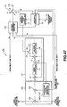
- the first integrator 11 shown in Fig.2 may be configured as a first integrator 51 fitted with a limiter, as shown in Fig.21 .
- This first integrator 51 fitted with the limiter limits the integrated value of the first integrator to a value equal to an integer number times the maximum amplitude level value.
- the switching controller 48 clears the cumulative addition value of the cumulative adder 46 to zero.
- the first integrator 51 fitted with the limiter is made up of an adder 52, a shifter 53 and a limiter 54, and feeds back an output limited by the limiter 54 to the adder 52.
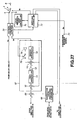
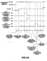
- This sixth embodiment is directed to a digital signal processing device 55 which, if an input original 1-bit signal S P contains an uncorrectable burst error, fades-out the 1-bit signal directly before the burst error using a fade-in device 60, and fades-in the signal directly after the burst error, thus muting the 1-bit signal during the period of occurrence of the burst error.
- This digital signal processing device 55 includes an error detector 57 for detecting the uncorrectable burst error contained in the original 1-bit signal S P supplied from an input terminal 56, a delay line 58 arranged downstream of the error detector 57 for delaying the original 1-bit signal S P and a fade-out/fade-in device 60 for fading-out and fading-in the delayed 1-bit signal S S from the delay line 58.
- the digital signal processing device 55 also includes a muting controller 59 which, on detection by the error detector 57 of the uncorrectable burst error in the original 1-bit signal S P , immediately fades-out the delayed 1-bit signal lying directly before the uncorrectable burst error in the delayed 1-bit signal S S from the delay line 58, using the fade/out/in device 60, and fades-in the delayed 1-bit signal immediately after the burst error to the maximum amplitude level using the fade-out/in device 60.
- a muting controller 59 which, on detection by the error detector 57 of the uncorrectable burst error in the original 1-bit signal S P , immediately fades-out the delayed 1-bit signal lying directly before the uncorrectable burst error in the delayed 1-bit signal S S from the delay line 58, using the fade/out/in device 60, and fades-in the delayed 1-bit signal immediately after the burst error to the maximum amplitude level using the fade-out/in device 60.
- the digital signal processing device 41 as shown in Fig.18 may be used.
- the amplitude controller 35 is actuated.
- the switching controller 48 switches the delayed ⁇ modulated signal from the delay line 3 to the ⁇ re-modulated signal from the ⁇ modulator 31
- the amplitude controller 35 controls the amplitude level of the level adjustment signal in order to execute the fade-out processing.
- the amplitude controller 35, level difference detector 42, cumulative adder 46 and the subtraction value control gate 47 are actuated.
- the switching controller 48 switches the ⁇ re-modulated signal to the delayed ⁇ modulated signal after the end of subtraction of the cumulative sum in the subtraction value control gate 47 with the aid of the changeover switch 4, the amplitude controller 35, level difference detector 42, cumulative adder 46 and the subtraction value control gate 47 execute the fade-in processing.
- the operation of the digital signal processing device 55 is explained by referring to the timing chart of Fig.24 .
- the error detector 57 If, in a system for transmitting or recording the original 1-bit signal S P , an uncorrectable burst error is produced, the error detector 57 generates an error period detection signal S Q specifying the error period. On reception of error period detection signal S Q , the muting processor 59 sends a fade-out/in processing signal S H to the switching controller 48 in the fade-out/in device 60 shown in Fig.18 . In this fade-out/in processing signal SH, the transition has been made from the fade-out/in processing to the fade-out processing. After awaiting the pattern coincidence signal S T fed from the pattern coincidence detector 28, the switching controller 48 causes the changeover switch 4 to switch from the 1-bit signal S A to the ⁇ modulated output S B of the ⁇ modulator 31. The 1-bit signal S A corresponds to the original 1-bit signal S P delayed by the delay line 58 and then re-delayed by the delay line 3.
- the coefficient generator 36 in the amplitude controller 35 in the fade-out/in device 60 immediately causes transition of the coefficient from 1 to 0, and completes the transition before error data during the error period reaches the ⁇ modulator 31 through the delay line 58.
- the muting controller 59 causes transition of the fade-out/in signal to the fade-in processing side after delay by the delay line 58.
- the coefficient generator 36 in the amplitude controller 35 immediately causes transition from 0 to 1.
- the subtraction value processing controller 45 cumulatively sums the level difference detector output signal S L from the level difference detector 42 to be cumulatively summed by the cumulative adder 46, as explained with reference to Fig.19 .
- data D so far accumulated in the cumulative adder 46 is gradually discharged via the subtraction value control gate 47.
- This data D is subtracted by the subtractor 44 from the maximum amplitude level input signal to the ⁇ modulator 31 to supply the subtractor output S o to the ⁇ modulator 31.
- the switching controller 48 first awaits, after delay by the delay line 31, the oncoming of the pattern coincidence detection signal S T from the pattern coincidence detector 28, and subsequently causes the changeover switch 4 to switch from the ⁇ modulator output signal S B to the 1-bit signal S A .
- the 1-bit signal SA corresponds to the original 1-bit signal S S delayed from the ⁇ modulated signal S B and further delayed by the delay line 3.
- the 1-bit output signal of the fade-out/in device 60 is returned via the low-pass filter to an analog audio signal, muting processing, in which the signal level is reduced to a zero level under noise suppression, is realized.
- This seventh embodiment is directed to a digital signal processing device 65 switching between the original 1-bit delay signal S A and the 1-bit signal S B , obtained on ⁇ re-modulating the amplitude-controlled signal by a as ⁇ modulator having a local feedback loop 67 ( ⁇ modulator having a local feedback lop), as shown in Fig.25 .
- the ⁇ modulator having a local feedback loop 67 shown in Fig. .25 is used in place of the ⁇ modulator 31 of the digital signal processing device 41 of the fifth embodiment.
- the local feedback loop is a well-known technique.
- Fig.26 shows an arrangement in which two local feedback loops having two gain multipliers 76, 77 are applied to a five-order ⁇ modulator having five integrators shown in Fig.6 , as shown in Fig.7 .
- a ⁇ modulator having the local feedback loop 75 it is possible to optimize the quantization noise components in the audible range for setting a dynamic rang to a broader value.
- a switch 78 shown in Fig.27 is provided in a feedback loop of the ⁇ modulator having a local feedback loop 67 for controlling the switching timing by a local feedback loop controller 71.
- the above processing is done for suppressing the noise generated on switching between the ⁇ re-modulated signal obtained by ⁇ modulator having the local feedback loop 75 and the original 1-bit signal.
- the digital signal processing device 65 includes a delay line 3, the bit-length converter 5, the amplitude controller 35, the level difference detector 42, an adder 66, the ⁇ modulator having the local feedback loop 67, the changeover switch 4, a switching controller 72, a subtraction value processing controller 68 for each integrator, a pattern coincidence detector 70 and a local feedback loop controller 71.
- the operation of the digital signal processing device 65 is explained by referring to the timing chart of Fig.28 .
- the local feedback loop controller 71 turns the local feedback loop of the ⁇ modulator having a local feedback loop 67 off so as not to perform local feedback.
- the switching controller 72 On reception of a switching request signal S D for switching from the delayed original 1-bit signal S A to the ⁇ re-modulated signal S B , the switching controller 72 first detects the coincidence at the pattern coincidence detector 70 and subsequently causes the changeover switch 4 to switch from the delayed original 1-bit signal to the ⁇ re-modulated signal S B .
- the local feedback loop 71 turns the local feedback loop control signal on and, by turning the switch 78 on, shorts the local feedback loop of the ⁇ modulator having a local feedback loop 67 on to render local feedback active.
- the local feedback loop 71 turns the local feedback loop control signal off to turn the local feedback loop of the ⁇ modulator having a local feedback loop 67 off to stop local feedback.
- the switching controller 72 causes the changeover switch 4 to switch from the output S B of the ⁇ modulator having a local feedback loop 67 to the original 1-bit signal S A , after passing through the subtraction by the subtraction value processing controller 68 and pattern coincidence detection processing, for realizing the switching free of noise.
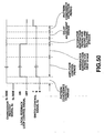
- This eighth embodiment is directed to a digital signal processing device 100 switching between two-channel ⁇ modulated signal, as an input signal obtained by two-channel ⁇ modulation, and the ⁇ re-modulated signal obtained from this input signal by a changeover switch as switching means, and executes cross-fading.
- This digital signal processing device 100 includes a ⁇ modulator 115 for setting the gain ratio between the first stage feedback loop and the second stage feedback loop to 16 and for outputting the ⁇ re-modulated 1-bit signal S B , and a delay line 102 for delaying a ⁇ modulated signal entered via an input terminal 101 by a first one of the above two channels a pre-set number of samples.
- This digital signal processing device 100 also includes a bit length converter 103 for matching the amplitude level of the ⁇ modulated signal to the amplitude level of the feedback signal to the first-stage integrator used in a ⁇ modulator 115 and an amplitude controller 104 for controlling the amplitude level of the a first level-adjusted signal having its amplitude level adjusted by-the bit length converter 103.
- the digital signal processing device 100 also includes a delay line 108 for delaying the other ⁇ modulated signal entered via an input terminal 101 by the second one of the above two channels a pre-set number of samples and a bit length converter 109 for matching the amplitude level of the other ⁇ modulated signal to the amplitude level of the feedback signal to the first-stage integrator used in the ⁇ modulator 115.
- the digital signal processing device 100 also includes an amplitude controller 110 for controlling the amplitude level of the second level-adjusted signal having its amplitude level adjusted by the bit length converter 109.
- the digital signal processing device 100 also includes an amplitude control output adjustment unit 105 comprised of a subtraction value processing controller for generating a signal for ⁇ re-modulation from two input/output signals of the amplitude controller 104 and the amplitude controller 110 and/or the signal in the ⁇ modulator 115 and for generation and subtraction of subtraction data obtained on the basis of the control processing during the amplitude control period.
- the digital signal processing device 100 further includes a switching controller 118 for controlling the amplitude controllers 104, 110, ⁇ modulator 115, amplitude control output adjustment unit 105 and the changeover switch 117.
- the ⁇ modulator 115 is a five-order ⁇ modulator comprised of five integrators configured as shown in Fig.6 , and is of the same configuration as the ⁇ -modulator 6 shown in Fig.7 .
- the gain ratio of the second-stage feedback loop to the state feedback loop excluding the integrator ahead and at back of the 1-bit quantizer in the ⁇ modulator 115 is an integer value of 16.
- the number of delay samples in the delay lines 102 and 108 is set to 16 for correspondence to this gain ratio of 16.
- the ⁇ modulator 115 may be a five-order ⁇ modulator comprised of five integrators configured as shown in Fig.9 , and may be configured as shown in Fig.19 .
- the initial value of the integrator enclosed within the ⁇ modulator 115 is set to 0.
- the digital signal processing device 100 also includes a pattern coincidence detection unit1 16 for detecting coincidence between the one and the other ⁇ modulated signals and the ⁇ re- modulated signals over plural samples and, based on the control signal obtained by the pattern coincidence detection unit 116 for switching between the one or the other ⁇ modulated signals S A and S C and the ⁇ re- modulated signals S B .
- the amplitude controller 104 is made up of a multiplier 121 and a coefficient generator 122, as shown in Fig.30 , and multiplies a first level-adjusted signal S I1 from the bit length converter 103 by a coefficient output S J1 from a coefficient generator 122 by the multiplier 121.
- the amplitude controller 104 then sends an amplitude controller output S K to the amplitude control output adjustment unit 105.
- the amplitude controller 110 is made up of a multiplier 123 and a coefficient generator 124, as shown in Fig.31 , and multiplies a second level-adjusted signal S I2 from the bit lenght converter 109 by a coefficient output S J2 from a coefficient generator 124 in the multiplier 123.
- the amplitude controller 110 then sends an amplitude controller output S V to the amplitude control output adjustment unit 105.
- the subtraction value processing controller in the amplitude control output adjustment unit 105 may be configured in many ways, as will be specifically described in the embodiments as later explained.
- Fig.32 shows, in a timing chart, the switching operation which the switching controller 118 causes the changeover switch 117 to perform when the cross-fading processing signal S H is supplied to the control signal input terminal 120 of Fig.29 .
- the switching controller 118 On reception of the cross-fading processing signal S H via the control signal input terminal 120, the switching controller 118 first awaits the pattern coincidence processing by the pattern coincidence detector 116, and subsequently sends the switch changeover signal S E to the changeover switch 117 in order to switch from the delayed original 1-bit signal S A of the first channel to the ⁇ re- modulated signals S B .
- a sum signal S X by the amplitude control output adjustment unit 105 of the amplitude controller output obtained with the coefficient of the coefficient generator 122 in the amplitude controller 104 set to 1 with the amplitude controller output S V obtained with the coefficient of the coefficient generator 124 in the amplitude controller 110 set to 0, is supplied to the ⁇ modulator 115.
- the switching controller 118 then causes transition of the coefficient generator output S J1 of the coefficient generator 122 in the amplitude controller 104 from 1 to 0, while causing transition of the coefficient generator output S J2 of the coefficient generator 124 in the amplitude controller 110 from 0 to 1.
- the amplitude control output adjustment unit 105 is fed with a gradually decreasing amplitude controller output S K and a gradually increasing amplitude controller output S V .
- the amplitude control output adjustment unit 105 sends a cross-faded addition signal S X to the ⁇ modulator 115.
- the subtraction data obtained on the basis of the control processing during the cross-fading period by the subtraction value processing controller in the amplitude control output adjustment unit 105 is gradually subtracted from the addition signal or from within ⁇ modulator 115.
- the amplitude control output adjustment unit 105 On termination of the subtraction operation, the amplitude control output adjustment unit 105 first awaits the pattern coincidence processing in the pattern coincidence detector 116 and sends the switch changeover signal S E to the changeover switch 117 to switch from the ⁇ re-modulator output S B to the delayed original 1-bit signal S C of the second channel.
- the listener can hear the sound cross-faded from the original audio signal of the first channel to the original audio signal of the second channel with noise suppression.
- This ninth embodiment is directed to a digital signal processing device 131 for realizing fade-in from a muted pattern signal and fade-out to the muted pattern signal by cross-fading a 1-bit muted pattern signal and a 1-bit signal obtained by ⁇ modulation.
- This digital signal processing device 131 has a mute pattern signal generator 132 for generating a mute pattern signal connected to the input terminal 101 of the digital signal processing device 100 of the above-described eighth embodiment. Therefore, parts or components excluding mute pattern signal generator 132 are depicted by the same numerals as those of the eighth embodiment and are not specifically explained.
- the operation of the digital signal processing device 131 is explained for the case of performing fade-in processing from a muting processing and for the case of performing muting processing from the fade-out processing.
- the digital signal processing device 131 receiving a fade-in processing signal S H1 via control signal input terminal 120 performs cross-fading from the mute pattern signal obtained by the mute pattern signal generator 132 supplied to the input terminal 101 to the ⁇ modulated signal supplied to the input terminal 107.
- This cross-fading processing is similar to that of the above-described eighth embodiment and hence is not explained specifically.
- the digital signal processing device 100 receiving a fade-out processing signal S H2 . via switching control terminal 120 performs cross-fading processing from the ⁇ modulated signal supplied to the input terminal 107 to the mute pattern signal obtained by the mute pattern signal generator 132 supplied to the input terminal 101.
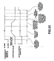
- This tenth embodiment is also a digital signal processing device for switching between two-channel ⁇ modulated signals as input signals obtained by the two-channel ⁇ modulation processing, and the ⁇ re-modulated signal derived from this input signal, and performs cross-fading.
- This tenth embodiment differs from the eighth embodiment shown in Fig.29 in arranging the amplitude control output adjustment unit 105 of the digital signal processing device 100 of the eighth embodiment as shown in Fig.34 and is otherwise the same as the eighth embodiment.
- the amplitude control output adjustment unit 105 includes a level difference detector 106 for detecting the difference between the first level adjustment signal from the bit length converter 103 and the level of the amplitude control output by the amplitude controller 104, and a cumulative adder 111 for cumulatively adding the level difference S u from the level difference detector 106 and the amplitude control output S v for the amplitude level control period for the first and second level-adjusted signals over the amplitude level width length of the first and second level-adjusted signals.
- the amplitude control output S v is an amplitude-controlled second level-adjusted signal from the bit length converter 109 outputted by the amplitude controller 110.
- the amplitude control output adjustment unit 105 also includes a subtraction value processing control gate 112 for gradually subtracting the cumulative sum S M of the cumulative adder 111 from the first and second level-adjusted signals using the adder/subtractor 114.
- the cumulative adder 111 and the subtraction value processing control gate 112 make up a subtraction value processing controller 113.
- the amplitude control output adjustment unit 105 is otherwise similar to the arrangement shown in Fig.29 .
- the timing chart for switching control performed by the switching controller 118 for the changeover switch 117 is similar to that of Fig.32 .
- Fig.35 shows, by an overall timing chart, the cross-fading processing operation by the present digital signal processing device 134.
- a switching controller 118 awaits the pattern coincidence processing by the pattern coincidence detector 116, and subsequently sends a switch changeover signal S E to the changeover switch 117 to switch from the delayed original 1-bit signal S A of the first channel to the ⁇ A modulator output S B .
- an addition signal S X by the adder/subtractor 114 in the amplitude control output adjustment unit 105 of the amplitude controller output S K, obtained with the coefficient of the coefficient generator 122 in the amplitude controller 104 set to 1, and the amplitude controller output S V obtained with the coefficient of the coefficient generator 124 in the amplitude controller 110 set to 0, are fed to the ⁇ modulator 115.
- the switching controller 118 causes transition of the coefficient generator output S J1 of the coefficient generator 122 in the amplitude controller 104 from 1 to 0, while causing transition of the coefficient generator output S J2 of the coefficient generator 124 in the amplitude controller 110 from 0 to1.
- the level difference detector 106 detects the difference S U between the amplitude level of the level adjustment signal S I1 (maximum amplitude level) and the input signal level to the adder/subtractor 114.
- the switching controller 118 controls the cumulative adder 111 for cumulatively adding the level difference S U and the output S V of the amplitude controller 110.
- the switching controller 118 causes the adder/subtractor 114 to gradually subtract the data SM, accumulated in the cumulative adder 111, from the amplitude controller outputs S K and S V via the subtractor control gate 112.
- the switching controller 118 controls the switching from the ⁇ modulator output S B to the delayed original 1-bit signal S C of the second channel through the pattern coincidence processing following delay of a pre-set number of samples.
- a first integrator 51 having a limiter shown in Fig.21 is substituted for the first integrator of the ⁇ modulator115, and the limiter value is set to an integer number times the maximum amplitude level width.
- control is managed so that the cumulative sum value in the cumulative adder 111 is cleared to zero by the switching controller 118.
- the listener can hear the cross-faded sound from the original audio signal of the first channel to the original audio signal of the second channel with noise suppression.
- This eleventh embodiment is directed to a digital signal processing device 135 configured for switching between two-channel ⁇ modulated signal as an input signal obtained by the two-channel ⁇ modulation processing, and ⁇ re-modulated signal derived from this input signal, and performs cross-fading.
- This tenth embodiment differs from the eighth embodiment shown in Fig.29 in substituting the an amplitude control output adjustement until 136 for the amplitude control output adjustement.
- unit 105 of the digital signal processing device 100 of the eighth embodiment shown in Fig.29 and is otherwise the same as the eighth embodiment.
- the amplitude control output adjustment unit 136 includes a level difference detector 137 for detecting the difference between the above second level adjustment signal and the level following amplitude control by the amplitude controller 110, and a cumulative adder 138 for cumulatively adding the level difference from the level difference detector 137 and the level following control of the amplitude level of the first level adjustment signal by the amplitude controller 104 with the amplitude level width length during the period of amplitude level control of the first and second level-adjusted signals.
- the amplitude control output adjustment unit 136 also includes a subtraction value control gate 139 for gradually subtracting the cumulative sum of the cumulative adder 138 from the first and second level adjustment signals using the adder/subtractor 141.
- the cumulative adder 138 and the subtraction value control gate 139 make up a subtraction value processing controller 140. Since the various components of the amplitude control output adjustment unit 136 are similar to those of the amplitude control output adjustment unit 100, the corresponding description in not made.
- the cross-fading processing operation performed by the digital signal processing device 135 is explained by referring to the timing chart of Fig. 37 .
- the timing chart for switching control performed by the switching controller 18 is similar to that shown in Fig.32 .
- the switching controller 118 receiving the cross-fading processing signal via switching control terminal 120 awaits the pattern coincidence processing at the pattern coincidence detector 116 and sends a switch changeover signal S E to the changeover switch 117 in order to switch from the delayed 1-bit signal S A of the first channel to the ⁇ modulator output S B .
- ⁇ modulator 115 To the ⁇ modulator 115 is sent the addition signal S X by the adder/subtractor 114 of the amplitude controller output S K obtained with the coefficient of the coefficient generator 122 in the amplitude controller 104 set to 1 and the amplitude controller output S V obtained with the coefficient of the coefficient generator 124 in the amplitude controller 110 set to 0.
- the switching controller 118 then causes transition of the coefficient generator output S J1 of the coefficient generator 122 in the amplitude controller 104 from 1 to 0, while causing transition of the coefficient generator output S J2 of the transition of the coefficient generator output S J2 of the coefficient generator 124 in the amplitude controller 110 from 0 to 1.
- the level difference detector 137 detects the difference S U of the input signal level to the adder/substractor 141 with respect to the amplitude level of the level-adjusted signal S 12 (maximum amplitude level).
- the switching controller 118 controls the cumulative adder 138 for cumulatively adding the level difference S U to the output S K of the amplitude controller 104.
- the switching controller 118 gradually subtracts the data S M accumulated in the cumulative adder 138 by the adder/subtractor 141 from the amplitude controller output S K and the amplitude controller output S V through the subtraction control gate 139.
- the switching controller 118 controls the switching from the ⁇ modulator output S B to delayed original 1-bit delay signal S C through pattern coincidence processing following delay over a pres-set number of samples.
- a first integrator 51 having a limiter 51 shown in Fig.21 is substituted for the first integrator of the ⁇ modulator115, and the limiter value is set to an integer number times the maximum amplitude level width.
- control is managed so that the cumulative sum value in the cumulative adder 111 is cleared to zero by the switching controller 118.
- the listener can hear the noise-suppressed cross-faded sound cross-faded from the original audio signal of the second channel.
- This twelfth embodiment is directed to a digital signal processing device configured for switching between two-channel ⁇ modulated signal as an input signal obtained by the two-channel ⁇ modulation processing, and a ⁇ re-modulated signal derived from this input signal, by the changeover switch 117 as switching means, and performs cross-fading.
- This twelfth embodiment differs from the eighth embodiment shown in Fig.29 in substituting the amplitude control output adjustment unit 143 for the amplitude control output adjustment unit 105 of the digital signal processing device 100 of the eighth embodiment shown in Fig.29 and in substituting a switching controller 154 for the switching controller 118.
- the present twelfth embodiment is otherwise the same as the eighth embodiment.
- the amplitude control output adjustment unit 143 includes a remainder detector 149 for detecting the remainder of the integrated value S ⁇ of a first integrator 153 in the ⁇ modulator 151 with respect to the maximum amplitude level width (equal to twice the above maximum amplitude level) and a subtraction value detector 147 for gradually subtracting the remainder detected by the remainder detector 149 from the maximum amplitude level signal outputted by the adder 144 using an adder./subtractor 145.
- the remainder detector 149 and the subtraction value detector 147 make up a subtraction value processing controller 146.
- the ⁇ modulator 151 is configured similarly to the ⁇ modulator 6 shown in Fig.7 and is comprised of a first coefficient multiplier connected downstream of a first adder 152 and the first integrator 153.
- the integrated value outputted by the first integrator 153 is supplied to the remainder detector 149 in the subtraction value processing controller 146.
- the switching controller 154 controls the amplitude controllers 104, 110, ⁇ modulator 151, amplitude control output adjustment unit 143 and the changeover switch 117, and is particularly characterized in that a subtraction value detection timing generator 155, generating a subtraction value detection timing signal, is provided in the subtraction value processing controller 146 in the amplitude output adjustment unit 143.
- the switching controller 154 receiving the cross-fading processing signal via switching control terminal 120 awaits the pattern coincidence processing at the pattern coincidence detector 116 and sends a switch changeover signal S E to the changeover switch 117 in order to switch from the delayed 1-bit signal S A of the first channel to the ⁇ modulator output S B .
- ⁇ modulator 151 To the ⁇ modulator 151 is sent the addition signal S X by the adder 144 of the amplitude controller output S K obtained with the coefficient of the coefficient generator 122 in the amplitude controller 104 of Fig.26 set to 1 and the amplitude controller output S V obtained with the coefficient of the coefficient generator 124 in the amplitude controller 110 set to 0.
- the switching controller 154 then causes transition of the coefficient generator output S J1 of the coefficient generator 122 in the amplitude controller 104 from 1 to 0, while causing transition of the coefficient generator output S J2 of the coefficient generator 124 in the amplitude controller 110 from 0 to 1.
- the subtraction value detection timing generator 155 in the switching controller 154 generates a subtraction value detection timing signal.
- the subtraction value control gate 147 is responsive to the subtraction value detection timing signal to seize a remainder S ⁇ from the remainder value detector 149.
- the subtraction value control gate 147 is responsive to the subtraction value detection timing signal to seize the remainder S ⁇ and causes he subtractor 145 to gradually subtract The remainder value from the addition signal S X .
- the switching controller 154 controls the switching from the ⁇ modulator output S B to the delayed original 1-bit signal S C of the second channel through the pattern coincidence processing following delay of a pre-set number of samples.
- This thirteenth embodiment is directed to a digital signal processing device configured for switching between two-channel ⁇ modulated signal as an input signal obtained by the two-channel ⁇ modulation processing, and ⁇ re-modulated signal derived from this input signal, by a changeover switch as switching means, and performs cross-fading.
- This thirteenth embodiment differs from the eighth embodiment shown in Fig.29 in substituting the an amplitude control output adjustment unit 158 for the amplitude control output adjustment unit 105 of the digital signal processing device 100 of the eighth embodiment shown in Fig.29 and is otherwise the same as the eighth embodiment.
- the amplitude control output adjustment unit 158 includes an adder 163 for adding the positive maximum amplitude level from the maximum amplitude level generator 162 to the integrated value S ⁇ of the first integrator 153 in the ⁇ modulator 151, and a remainder value detector 164 for detecting the remainder value relative the maximum amplitude level (equal to the above maximum amplitude level) of the addition output of the adder 163.
- the amplitude control output adjustment unit 158 also includes a subtractor 165 for subtracting the positive maximum amplitude level from the remainder value detected by the remainder value detector 164, and a subtraction value control gate 166 for gradually subtracting the subtraction output of the subtractor 165 from the maximum amplitude level signal outputted by the adder 159 using the adder/subtractor 160.
- the subtraction output is termed thereinafter as the result of subtraction of the addition remainder value.
- the adder 163, remainder value detector 164, subtraction value control gate 166 and a maximum amplitude level generator 162 make up a subtraction
- Fig.40 showing signal examples of the integration value S ⁇ and the result of subtraction of the addition remainder value S ⁇ in the case of binary processing.
- the switching controller 154 receiving the cross-fading processing signal via switching • control terminal 120 awaits the pattern coincidence processing at the pattern coincidence detector 116 and sends a switch changeover signal S E to the changeover switch 117 in order to switch from the delayed 1-bit signal S A of the first channel to the ⁇ modulator output S B .
- ⁇ modulator 151 To the ⁇ modulator 151 is sent, via a subtractor 160, an addition signal S X by the adder 159 of the amplitude controller output S K obtained with the coefficient of the coefficient generator 122 in the amplitude controller 104 of Fig.30 set to 1 and the amplitude controller output S V obtained with the coefficient of the coefficient generator 124 in the amplitude controller 110 set to 0.
- the switching controller 118 then causes transition of the coefficient generator output S J1 of the coefficient generator 122 in the amplitude controller 104 from 1 to 0, while causing transition of the coefficient generator output S J2 of the coefficient generator 124 in the amplitude controller 110 from 0 to 1.
- the subtraction value detection timing generator 155 in the switching controller 154 generates a subtraction value detection timing signal.
- the subtraction value control gate 166 is responsive to the subtraction value detection timing signal to seize the remainder S ⁇ from the remainder value detector 165.
- the result of subtraction of the addition remainder value S ⁇ is now explained.
- the first integrator 153 of the ⁇ modulator 151 outputs an integrated value S ⁇ shown in Fig.40 . It is assumed that the maximum amplitude level width is 1000 (binary) as a power of 2. Then, by detecting the lower 3 bits and recognizing them as a 2's complement, the detection value directly becomes the result of subtraction of the addition remainder value S ⁇ obtained on subtracting the positive maximum amplitude level from the remainder value corresponding to addition of the positive maximum amplitude level.
- the subtraction value control gate 166 seizes the result of subtraction of the addition remainder value S ⁇ responsive to the subtraction value detection timing signal and gradually subtracts the result S ⁇ from the addition signal S X .
- the switching controller 154 controls switching from the ⁇ modulator output S B to the delayed original 1-bit signal S C of the second channel through the pattern coincidence processing following delay over a pre-set number of samples.
- the 1-bit output signal outputted at an output terminal of the digital signal processing device of the thirteenth embodiment is restored via a low-pass filter to an analog audio signal, cross-fading from the original audio signal of the first channel to the original audio signal of the second channel with noise suppression is realized.
- the time of convergence to zero may be halved for realizing smoother switching.
- a fourteenth embodiment is explained, in which the first integrator 51 having the limiter shown in Fig. 21 is substituted for the first integrator 153 of the- ⁇ EA--modulator-151-iri--the digital signal processing device of the above-described twelfth embodiment, is explained.
- This fourteenth embodiment is directed to a digital signal processing device for causing a changeover switch 117, as switching means, to switch between the two-channel ⁇ modulated signal, as an input signal obtained by the two-channel ⁇ modulation, and ⁇ re-modulated signal derived from the input signal, and performs cross-fading.
- a first integrator having a limiter 151 for preventing dispersion in the ⁇ modulator 151.
- the integrated value S ⁇ is supplied to a remainder value detector 149 in the subtraction value controller 146 shown in Fig.38 .
- a switching controller 154 shown in Fig.41 awaits the pattern coincidence processing by the pattern coincidence detector 116, and subsequently sends a switch changeover signal S E to the changeover switch 117.
- the changeover switch switches from the delayed original 1-bit signal S A of the first channel to the ⁇ modulator output S B .
- the digital signal processing device causes the subtraction value control gate 147 to gradually subtract, from the maximum amplitude level signal, the remainder value S ⁇ from the maximum amplitude level width of the limiter integrated value S ⁇ during the period of selection of the delayed original 1-bit signal, using the subtractor 145.
- an addition signal S X by the adder/subtractor 144 in the amplitude control output adjustment unit 144 of the amplitude controller output S K obtained with the coefficient of the coefficient generator 122 in the amplitude controller 104 of Fig.30 set to 1 and the amplitude controller output S V obtained with the coefficient of the coefficient generator 124 in the amplitude controller 110 set to 0, is fed via subtractor 145 to the ⁇ modulator 151.
- the switching controller 154 causes transition of the coefficient generator output S J1 of the coefficient generator 122 in the amplitude controller 104 from 1 to 0, while causing transition of the coefficient generator output S J2 of the coefficient generator 124 in the amplitude controller 110 from 0 tol.
- the subtraction value detection timing generator 155 in the switching controller 154 generates a subtraction value detection timing signal.
- the subtraction value control gate 147 is responsive to the subtraction value detection timing signal to seize a remainder S ⁇ from the remainder value detector 149.
- the subtraction value control gate 147 is responsive to the subtraction value detection timing signal to seize the remainder S ⁇ and causes the subtractor 145 to gradually subtract the remainder value from the addition signal S X .
- the switching controller 154 controls the switching from the ⁇ modulator output S B to the delayed original 1-bit signal S C of the second channel through the pattern coincidence processing following delay of a pre-set number of samples.
- the digital signal processing device has a first integrator 51 having a limiter for limiting the integrated value of the ⁇ modulator 151 with a limit value of an integer number multiple, such as four times, of the maximum amplitude level width.
- the limit values of the first integrator having the limiter 51 become 0100000 and 1100000. This sets the remainder from the maximum amplitude level width during operation of the first integrator 51 having the limiter to 0.
- subtraction of the remainder value from the maximum amplitude level by the subtraction control gate 147 prior to switching control to the ⁇ re-modulated 1-bit signal, required with the digital signal processing device according to the fourteenth embodiment, is not required, such that cross-fading from the original audio signal of the first channel to the original audio signal of the second channel under noise suppression is realized even on limiter operation.
- a fifteenth embodiment in which the ⁇ modulator 151 shown in Fig.21 is substituted for the first integrator 153 of the ⁇ modulator 151 of the digital signal processing device according to the thirteenth embodiment, is explained.
- the present fifteenth embodiment is directed to a digital signal processing device having a changeover switch 117 as switching means for switching between the two-channel ⁇ modulated signal as an input signal obtained by the two-channe ⁇ modulation and the ⁇ re-modulated signal derived from the input signal, and executes cross-fading.
- the present fifteenth embodiment has a first integrator having limiter 51 for preventing dispersion of the ⁇ modulator 151.
- the integrated value S ⁇ is supplied to a remainder value detector 163 in the amplitude control output adjustment unit 158 shown in Fig.39 .
- the switching controller 154 On reception of the cross-fading signal S H via control signal input terminal 120, the switching controller 154 awaits the pattern coincidence processing by the pattern coincidence detector 116, and subsequently sends a switch changeover signal S E to the changeover switch 117.
- the changeover switch switches from the delayed original 1-bit signal S A of the first channel to the ⁇ modulator output S B .
- the digital signal processing device gradually subtracts, from the maximum amplitude level signal entering the ⁇ modulator 151, the remainder value S ⁇ from the maximum amplitude level width of the limiter integrated value S ⁇ during the period of selection of the delayed original 1-bit signal, using the subtractor 160.
- This result of subtraction of addition remainder value S ⁇ is obtained by detecting, by the remainder value detector 164, the remainder value from the maximum amplitude level width of an addition signal obtained on adding the positive maximum amplitude level by the adder 163 to the limiter integrated value S ⁇ of first integrator 51 having the limiter, and by subtracting the maximum signal level by the subtractor 165.
- an addition signal S X by the adder 159 of the amplitude controller output S K obtained with the coefficient generator output S J1 of the coefficient generator 122 in the amplitude controller 104 of Fig.30 set to 1 and the amplitude controller output S V obtained with the coefficient of the coefficient generator 124 in the amplitude controller 110 set to 0, is fed via subtractor 160 to the ⁇ modulator 151.
- the switching controller 154 causes transition of the coefficient generator output S J1 of the coefficient generator 122 in the amplitude controller 104 from 1 to 0, while causing transition of the coefficient generator output S J2 of the coefficient generator 124 in the amplitude controller 110 from 0 tol.
- the subtraction value detection timing generator 155 in the switching controller 154 generates a subtraction value detection timing signal.
- the subtraction value control gate 166 is responsive to the subtraction value detection timing signal to seize the remainder S ⁇ .
- the subtraction value control gate 166 then gradually subtracts the remainder S ⁇ from the addition signal S X by the subtractor 160.
- the switching controller 154 controls the switching from the ⁇ modulator output SB to the delayed original 1-bit signal S C of the second channel through the pattern coincidence processing following delay of a pre-set number of samples.
- the time of convergence to zero may be halved for realizing smother switching.
- the digital signal processing device of the present fifteenth embodiment by setting the limit value of the first integrator having the limiter 151 to an integer number times, such as four times, the maximum amplitude level width, subtraction of the result of subtraction of the addition remainder value S ⁇ from the maximum amplitude level 1 by the subtraction control gate 166 prior to switching control to the ⁇ re-modulated 1-bit signal, is not required, such that cross-fading from the original audio signal of the first channel to the original audio signal of the second channel under noise suppression is realized even on limiter operation.
- the present sixteenth embodiment is directed to an arrangement of a switching device for two-channel ⁇ modulated signal of the eighth embodiment in which, for constructing a subtraction value processing controller within the amplitude control output adjustment unit in Fig.29 , a remainder value detector is provided within the amplitude control output adjustment unit.
- the present embodiment is directed to such a device corresponding to the twelfth, thirteenth and fourteenth embodiments in which not only the integrated value of the first integrator but also the integrated values of the second and following integrators are used for controlling the subtraction of the integrated value in the integrator in each ⁇ modulator in each digital signal processing device.
- Fig.43 shows an illustrative device for controlling the processing of subtraction values for the second and following integrators.
- Control outputs returned from the second subtraction value processing controller 172 through to the fifth subtraction value processing controller 175 are returned to the adders 13 through to 22 provided ahead of the integrators of the second and following stages of the integrators.
- subtraction value processing control occurs sequentially after subtraction processing in the first-stage first subtraction value processing controller 171 completely comes to a close.
- the switching controller 171 supplying pulsed subtraction value processing control signals to the subtraction value processing controllers 171 through to 175 at the timing shown in Fig.44 .
- the switching controller 171 supplying pulsed subtraction value processing control signals to the subtraction value processing controllers 171 through to 175 at the timing shown in Fig.44 .
- limiting processing becomes possible for the second and the following stages of the integrators by similar subtraction processing by the integrators with the limiters.
- limit values of the entire integrators are set to a value equal to an integer number times of the maximum amplitude level value, limiting processing free of subtraction is also realized. This may be applied to the tenth and eleventh embodiments.
- This seventeenth embodiment is directed to a digital signal processing device 125 designed for switching between two-channel ⁇ modulated signals S A , S C and a 1-bit signal S B obtained on ⁇ re-modulating a signal S X by a ⁇ modulator 67 having a local feedback loop shown in Fig.26 .
- the signal S X is obtained by amplitude-controlling these two-channel ⁇ modulated signals S A , S C .
- the basic arrangement is similar to that of the digital signal processing device 100 shown in Fig.29 .
- the arrangement of the ⁇ modulator and the peripheral circuitry are also shown in Fig.47 .
- the present digital signal processing device 125 includes two delay lines 102, 108, two bit length converters 103, 109, two amplitude controllers 104, 110 and an amplitude control output adjustment unit 105.
- the present digital signal processing device 125 also includes a ⁇ modulator having a local feedback loop 67, a changeover switch 117, a switching controller 72, subtraction value processing controllers 68, 69 for the integrators, a pattern coincidence detector 116 and a local feedback loop controller 71.
- the arrangement of the ⁇ modulator having a local feedback loop 67 and the subtraction value processing controller in the amplitude control output adjustment unit may be configured as the ⁇ modulator having a local feedback loop 67 in the digital signal processing devices 173, 174 and 175 and the amplitude control output adjustment units 105, 143 and 176 shown in Figs.46 to 48 .
- a switch 78 for opening/closing the local feedback loop.
- the local feedback loop controller 71 opens the switch 78 for turning off the local feedback loop of the ⁇ modulator having a local feedback loop 67 to inhibit local feedback.
- the switching controller 72 On reception of the switching request signal S H for switching from the original 1-bit signal S A from the original 1-bit signal S B for cross-fading, the switching controller 72 first detects pattern coincidence in the pattern coincidence detector 116 and then receives the switch control signal S E to cause the changeover switch 117 to switch from the original 1-bit signal S A to the signal S B of the ⁇ modulator having a local feedback loop 67.
- the local feedback loop controller 71 turns on the switch 78 to complete the local feedback loop of the ⁇ modulator having a local feedback loop 67 to activate local feedback. Subsequently, the local feedback loop controller 71 undergoes the amplitude processing by the amplitude controllers 104, 110 to reach respective gain values of 0 and 1, respectively. The local feedback loop controller 71 then receive a switching request to the original 1-bit signal S C from the ⁇ re-modulated signal S B to turn off the switch 78 to open the local feedback loop of the ⁇ modulator having a local feedback loop 67 to terminate local feedback.
- the switching controller 72 receives the switching control signal S E following subtraction processing by the subtraction value processing controller and the pattern coincidence detection processing, for realization of the noise-free switching, and causes the changeover switch 117 to switch from tne ⁇ re-modulated signal S ⁇ to the original 1-bit signal S C .
- the listener can hear high-quality cross-faded sound from the original audio signal of the first channel to the original audio signal of the second channel.
- Fig.50 illustrates, by a timing chart, another example of the on-of control by the switch 78 of local feedback of the ⁇ modulator having a local feedback loop 67 by the local feedback loop controller 71.
- the operation up to activation of the local feedback loop is the same as that shown in Fig.49 .
- the switching controller 72 receives a switching request to the original 1-bit signal S C from the ⁇ re-modulated signal S B to perform subtraction processing for the first-stage integrator by the subtraction value processing controller or the first subtraction value processing controller 171.
- the local feedback loop controller 71 then turns off the local feedback loop control signal and turns off the switch 78 to open the local feedback loop of the ⁇ modulator having a local-feedback loop 67 to terminate local feedback. If the device has second and following stages of the integrators as shown in Fig.48 , the local feedback loop controller 71 sequentially performs subtraction processing for the second and following stages of the integrators by the second and following stages of the subtraction value processing controllers and undergoes the pattern coincidence detection processing to receive the switch control signal S E to switch from the output S B of the ⁇ re-modulator having local feedback loop to the original 1-bit signal S C .
- the control of the local feedback lop at the timing shown in Fig.50 is effective for a modulator, as ⁇ modulator having a local feedback loop 67, in which the local feedback loop is not connected to a point ahead of the initial stage integrator 11, such as a five-order ⁇ modulator shown for example in Fig.26 .
- This realizes a ⁇ re-modulated signal having a local feedback loop until directly before switching.
- the ⁇ modulator having a local feedback loop 67 may be configured as shown in Fig.51 . That is, the feedback loop gain by the variable gain multiplier 82 of the ⁇ modulator having a local feedback loop 81 may be variably controlled by the local feedback loop controller 83.
- the exceptional case of the device having plural stages of the subtraction value processing controllers configured as shown in Fig.48 has been described in the above, this is not to be construed in the limiting sense.
- the local feedback loop controller 83 sets the loop gain value sent to the variable gain multiplier 82 of the local feedback loop of the ⁇ modulator having a local feedback loop 81 to zero without performing local feedback.
- the switching controller 72 On reception of the switching request signal S H from the original 1-bit signal S A to the signal S C , for cross-fading, the switching controller 72 first detects the pattern coincidence at the pattern coincidence detector 70 and then receives the switching control signal S E to cause the changeover switch 117 to switch from the original 1-bit signal S A to the output S B of the ⁇ modulator having local feedback loop.
- the local feedback loop 83 gradually varies the loop gain value to the variable gain multiplier 82 to a stationary loop gain value for activating the feedback to the ⁇ modulator having local feedback loop. 81. If, after the gain values are restored to 0 and 1 through the amplitude processing performed by the amplitude controllers 104, 110, respectively, the switching controller 72 receives a switching request from the ⁇ re-modulated signal S B to the original 1-bit signal S C , the switching controller 72 performs subtraction processing for the first-stage integrator by the subtraction value processing controller or the first subtraction value processing controller 171 for realizing noise-free switching.
- the local feedback loop controller 83 gradually diminishes the loop gain value to the variable gain multiplier 82 and ultimately to zero for opening the local feedback loop for terminating local feedback. If the device has second and following stages of the subtraction value processing controllers after cessation of the processing and local feedback, the local feedback loop controller 83 receives the switch control signal S E after sequentially performing subtraction processing for the second and following stage integrators by the second and following stage subtraction value processing controller 172 and the pattern coincidence detection processing to cause the switch 117 to switch from the output S B of the ⁇ modulator having local feedback loop 81 to the original 1-bit signal S C .
- the digital signal processing device 65 it is assumed that two local feedback loops are controlled simultaneously by an arrangement in which the five-order ⁇ modulator has two local feedback loops.
- the same effect may be realized by controlling only the input side feedback loop.
- the similar effect may also be realized by setting the opening timing of the downstream side local feedback loop so as to be temporally after the end of the subtraction processing for the integrator upstream of the integrator to which is connected the feedback loop.
- the five-order ⁇ modulator shown in Fig.26 is used in the digital signal processing device 65 as the ⁇ modulator having the local feedback loop, there is no limitation to the number of orders or the number of feedback loops.
- the ⁇ modulator having the local feedback loop may be configured as shown in Fig.51 for outputting variable loop gain from the local feedback controller 83 to the variable gain multiplier 82.
- the application shown as the switching device for an input obtained by a two-channel ⁇ modulator can be applied to a device for scanning the amplitude of an input signal obtained by a single-channel ⁇ modulation
Landscapes
- Physics & Mathematics (AREA)
- Nonlinear Science (AREA)
- Engineering & Computer Science (AREA)
- Theoretical Computer Science (AREA)
- Compression, Expansion, Code Conversion, And Decoders (AREA)
- Signal Processing Not Specific To The Method Of Recording And Reproducing (AREA)
- Control Of Amplification And Gain Control (AREA)
Claims (39)
- Digitalsignal-Verarbeitungsvorrichtung (1) zum Umschalten zwischen einem verzögerten sigma-delta-modulierten Signal (SA), welches durch Verzögern eines sigma-delta-modulierten Signals als Eingangssignal erlangt wird, und eines sigma-delta-zurückmodulierten Signals (SB), welches durch Sigma-Delta-Zurückmodulation des Eingangssignals erlangt wird, wobei die Vorrichtung umfasst:eine Eingangssignal-Verzögerungseinrichtung (3) zum Verzögern des Eingangssignals um eine vorher festgelegte Anzahl an Proben zum Ausgeben des verzögerten sigma-delta-modulierten Signals (SA):eine Sigma-Delta-Modulations-Verarbeitungseinrichtung (6), welche mehrere Integratoren (11, 14, 17, 20, 23) hat, um das sigma-delta-zurückmodulierte Signal (SB) auszugeben;eine Pegeleinstelleinrichtung (5) zum Einstellen des Amplitudenpegels des sigma-delta-modulierten Signals, welches in die Sigma-Delta-Modulations-Verarbeitungseinrichtung (6) eintritt, um den Amplitudenpegel eines Zurückführungssignals an einen erststufigen Integrator (11) anzupassen, der in der Sigma-Delta-Modulations-Verarbeitungseinrichtung (6) verwendet wird; undeine Schaltsteuereinrichtung (7) zum Steuern des Schaltens durch eine Schalteinrichtung (4).
- Digitalsignal-Verarbeitungsvorrichtung nach Anspruch 1, wobei ein Gewinnverhältnis zwischen einer erststufigen Zurückführungsschleife der Sigma-Delta-Modulations-Verarbeitungseinrichtung (6) und der nächststufigen Zurückführungsschleife eine ganze Zahl ist und wobei die vorher festgesetzte Anzahl an Proben der Eingangssignal-Verzögerungseinrichtung (3) auf Basis dieses Gewinnverhältnisses festgesetzt wird.
- Digitalsignal-Verarbeitungsvorrichtung nach Anspruch 1 oder 2, welche außerdem eine Musterübereinstimmungs-Erfassungseinrichtung (28) zum Erfassen der Übereinstimmung des verzögerten sigma-delta-modulierten Signals (SA) und des sigma-delta-zurückmodulierten Signals (SB) über mehrere Proben umfasst; wobei die Schaltsteuereinrichtung (29) die Schalteinrichtung auf Basis des Erfassungsergebnisses steuert, welches durch die Musterübereinstimmungs-Erfassungseinrichtung (28) erlangt wird.
- Digitalsignal-Verarbeitungsvorrichtung nach Anspruch 1, 2 oder 3,
wobei die Schaltsteuereinrichtung (29) den Anfangswert des Integrators der Sigma-Delta-Modulations-Verarbeitungseinrichtung (6) auf Null unmittelbar vor der Zuführung des Eingangssignals und/oder während der Zeit setzt, wo das verzögerte sigma-delta-modulierte Signal (SA) von der Eingangssignal-Verzögerungseinrichtung (3) durch Umschalten durch die Schalteinrichtung (4) ausgewählt wird. - Digitalsignal-Verarbeitungsvorrichtung nach Anspruch 1, 2, 3 oder 4, welche außerdem eine Amplitudensteuereinrichtung (35) zum Steuern des Amplitudenpegels eines pegel-eingestellten Signals (S1) aufweist, welches den Amplitudenpegel hat, der durch die Pegeleinstelleinrichtung eingestellt ist; wobei die Schaltsteuereinrichtung (48) veranlasst, dass die Amplitudensteuereinrichtung den Amplitudenpegel des pegel-eingestellten Signals steuert, nachdem veranlasst ist, dass die Schalteinrichtung von dem verzögerten sigma-delta-modulierten Signal von der Eingangssignal-Verzögerungseinrichtung auf das sigma-delta-zurückmodulierte Signal, welches bei der Sigma-Delta-Modulation des pegel-eingestellten Signals erlangt wird, umschaltet.
- Digitalsignal-Verarbeitungsvorrichtung nach Anspruch 1, 2, 3 oder 4, welche außerdem aufweist:eine Amplitudensteuereinrichtung (35) zum Steuern des Amplitudenpegels des pegel-eingestellten Signals, das einen Amplitudenpegel hat, der durch die Pegeleinstelleinrichtung (5) eingestellt ist;eine Pegeldifferenz-Erfassungseinrichtung (42) zum Erfassen der Differenz zwischen dem maximalen Amplitudenpegel des pegel-eingestellten Signals und dem Amplitudenpegel des Ausgangssignals, das auf die Amplitudensteuerung folgt, während der Zeit, wo die Amplitudensteuereinrichtung (35) den Amplitudenpegel des pegel-eingestellten Signals steuert;eine Kumulativ-Additionseinrichtung (46) zum kumulativen Addieren der Pegeldifferenz von der Pegeldifferenz-Erfassungseinrichtung mit einer maximalen Amplitudenpegel-Breitenlänge gleich dem zweifachen des maximalen Amplitudenpegels des pegel-eingestellten Signals; undeine Subtraktionssteuereinrichtung (47) zum graduellen Subtrahieren der kumulativen Summe der Kumulativ-Additionseinrichtung vom maximalen Amplitudenpegel des pegel-eingestellten Signals nach der Amplitudensteuerung in der Amplitudensteuereinrichtung (35);wobei die Schaltsteuereinrichtung (48) veranlasst, dass die Schalteinrichtung (4) vom sigma-delta-modulierten Signal auf das verzögerte sigma-delta-modulierte Signal nach dem Ende der Subtraktion der kumulativen Summe in der Subtraktionssteuereinrichtung (47) umschaltet.
- Digitalsignal-Verarbeitungsvorrichtung nach einem der vorhergehenden Ansprüche, wobei, wenn ein erster Integrator (51) der Sigma-Delta-Modulations-Verarbeitungseinrichtung mit einer Begrenzereinrichtung (54) bereitgestellt wird, um einen integrierten Wert des ersten Integrators (51) mit einem begrenzenden Wert zu begrenzen, der gleich einer ganzzahligen Häufigkeit der maximalen Amplitudenpegelbreite ist, die Schaltsteuereinrichtung (48) den kumulativen Summenwert der Kumulativ-Additionseinrichtung auf null während der Zeit löscht, wo die Begrenzereinrichtung (54) in einem Zustand arbeitet, bei dem der integrierte Wert größer ist als der Begrenzerwert.
- Digitalsignal-Verarbeitungsvorrichtung nach Anspruch 1, welche außerdem umfasst:eine Fehlererfassungseinrichtung (57) zum Erfassen eines nichtkorrigierbaren Burst-Fehlers im sigma-delta-modulierten Signal;eine Verzögerungseinrichtung (58), welche stromabwärts von der Fehlererfassungseinrichtung (57) vorgesehen ist, um das sigma-delta-modulierte Signal zu verzögern;eine Ausblendeinrichtung (60) zum Ausblenden des sigma-delta-modulierten Signals über die Verzögerungseinrichtung;eine Einblendeinrichtung (60) zum Einblenden des sigma-delta-modulierten Signals über die Verzögerungseinrichtung; undeine Steuereinrichtung (59), um zu veranlassen, dass die Ausblendeinrichtung das sigma-delta-modulierte Signal, welches durch die Verzögerungseinrichtung verzögert ist, bis unmittelbar vor einem nichtkorrigierbaren Burst-Fehler unmittelbar auf einen Nullpegel ausblendet, wenn die Fehlererfassungseinrichtung diesen nichtkorrigierbaren Burst-Fehler im sigma-delta-modulierten Signal erfasst, wobei die Steuereinrichtung veranlasst, dass die Einblendeinrichtung das sigma-delta-modulierte Signal unmittelbar nach dem Burst-Fehler bis zum maximalen Amplitudenpegel einblendet.
- Digitalsignal-Verarbeitungsvorrichtung nach Anspruch 8, wobei die Ausblendeinrichtung (60) eine Amplitudensteuereinrichtung zum Steuern des Amplitudenpegels des pegel-eingestellten Signals aufweist, welches den Amplitudenpegel hat, der durch die Pegeleinstelleinrichtung eingestellt ist;
wobei die Ausblendeinrichtung (60) veranlasst, dass die Amplitudensteuereinrichtung den Amplitudenpegel des pegel-eingestellten Signals steuert, um eine Ausblendverarbeitung auszuführen, nachdem die Schaltsteuereinrichtung veranlasst hat, dass die Schalteinrichtung von dem verzögerten sigma-delta-modulierten Signal von der Eingangssignal-Verzögerungseinrichtung auf das sigma-delta-zurückmodulierte Signal von der Sigma-Delta-Modulations-Verarbeitungseinrichtung umschaltet. - Digitalsignal-Verarbeitungsvorrichtung nach Anspruch 8, wobei die Einblendeinrichtung (60) umfasst:eine Amplitudensteuereinrichtung zum Steuern des Amplitudenpegels des pegel-eingestellten Signals, welches den Amplitudenpegel hat, der durch die Pegeleinstelleinrichtung eingestellt ist;eine Pegeldifferenz-Erfassungseinrichtung zum Erfassen der Differenz zwischen dem maximalen Amplitudenpegel des pegel-eingestellten Signals und dem Amplitudenpegel eines pegel-gesteuerten Ausgangssignals während der Zeit, wo die Amplitudensteuereinrichtung den Amplitudenpegel des pegel-eingestellten Signals steuert,eine Kumulativ-Additionseinrichtung zum kumulativen Addieren der Pegeldifferenz von der Pegeldifferenz-Erfassungseinrichtung mit einer maximalen Amplitudenpegel-Breitenlänge gleich dem Zweifachen des maximalen Amplitudenpegels des pegel-eingestellten Signals; undeine Subtraktionssteuereinrichtung zum graduellen Vermindern - nach der Amplitudensteuerung durch die Amplitudensteuereinrichtung - der kumulativen Summe der Kumulativ-Additionseinrichtung vom maximalen Amplitudenpegel des pegel-eingestellten Signals;wobei die Schaltsteuereinrichtung veranlasst, dass die Umschalteinrichtung vom sigma-delta-zurückmodulierten Signal auf das verzögerte sigma-delta-zurückmodulierte Signal nach dem Ende der Subtraktion der kumulativen Summe in der Subtraktionseinrichtung umschaltet, um das Einblenden auszuführen.
- Digitalsignal-Verarbeitungsvorrichtung nach einem der vorhergehenden Ansprüche, wobei die Sigma-Delta-Modulations-Verarbeitungseinrichtung (6) aufweist:mehrere Stufen seriell-geschalteter Integratoren (11, 14, 17, 20, 23); undeine lokale Zurückführungsschleife zum Zurückführen eines Ausgangssignals der mehrstufigen Integratoren zu Eingängen von Integratoren einer vorhergehenden Stufe.
- Digitalsignal-Verarbeitungseinrichtung (100), um zu veranlassen, dass eine Schalteinrichtung (117) zwischen einem zweikanaligen sigma-delta-modulierten Signal als Eingangssignal, welches durch eine zweikanalige Sigma-Delta-Modulations-Verarbeitungseinrichtung erlangt wird, und einem sigma-delta-zurückmodulierten Signal (SB), welches vom Eingangssignal abgeleitet wird, umschaltet, wobei die Einrichtung umfasst:eine Sigma-Delta-Modulations-Verarbeitungseinrichtung (115), welche mehrere Integratoren (11, 14, 17, 20, 23) hat, um das sigma-delta-zurückmodulierte Signal (SB) auszugeben;eine erste Eingangssignal-Verzögerungseinrichtung (102) zum Verzögern des sigma-delta-modulierten Signals eines ersten der beiden Kanäle um eine vorher festgesetzte Anzahl an Proben zum Ausgeben eines ersten verzögerten sigma-delta-modulierten Signals (SA);eine erste Pegeleinstelleinrichtung (103) zum Einstellen des Amplitudenpegels des sigma-delta-modulierten Signals eines ersten der beiden Kanäle, um den Amplitudenpegel des Zurückführungssignals an den erststufigen Integrator (11), der in der Sigma-Delta-Modulations-Verarbeitungseinrichtung (115) verwendet wird, anzupassen; undeine erste Amplitudensteuereinrichtung (104) zum Steuern des Amplitudenpegels eines ersten pegel-eingestellten Signals (S11), welches den Amplitudenpegel hat, der durch die erste Pegeleinstelleinrichtung (103) eingestellt ist;eine zweite Eingangssignal-Verzögerungseinrichtung (108) zum Verzögern des sigma-delta-modulierten Signals eines zweiten der beiden Kanäle um eine vorher festgesetzte Anzahl an Proben zum Ausgeben eines zweiten verzögerten sigma-delta-modulierten Signals (SC);eine zweite Pegeleinstelleinrichtung (109) zum Einstellen des Amplitudenpegels des sigma-delta-modulierten Signals eines zweiten der beiden Kanäle, um den Amplitudenpegel des Zurückführungssignals an den erststufigen Integrator (11), der bei der Sigma-Delta-Modulations-Verarbeitungseinrichtung (115) verwendet wird, anzupassen;eine zweite Amplitudensteuereinrichtung (110), um den Amplitudenpegel eines zweiten pegel-eingestellten Signals (S12) zu steuern, welches den Amplitudenpegel hat, der durch die zweite Pegeleinstelleinrichtung (109) eingestellt ist;eine Amplitudensteuer-Ausgangssignal-Einstelleinrichtung (105) zum Einstellen der Ausgangssignale der ersten Amplitudensteuereinrichtung (104) und der zweiten Amplitudensteuereinrichtung (110); undeine Schaltsteuereinrichtung (118) zum Steuern der ersten Amplitudensteuereinrichtung (104), der zweiten Amplitudensteuereinrichtung (110), der Sigma-Delta-Modulations-Verarbeitungseinrichtung (115), der Amplitudensteuer-Ausgangssignal-Einstelleinrichtung (105) und der Schalteinrichtung (117);wobei die Schaltsteuereinrichtung (118) nach dem Umschalten vom ersten sigma-delta-modulierten Signal (SA) auf das delta-zurückmodulierte Signal (SB) veranlasst, dass die erste Amplitudensteuereinrichtung (104), die zweite Amplitudensteuereinrichtung (110) und die Amplitudensteuer-Ausgangssignal-Einstelleinrichtung (105) Amplitudenpegel des sigma-delta-modulierten Signals (SA) und des anderen sigma-delta-modulierten Signals (SC) steuert.
- Digitalsignal-Verarbeitungsvorrichtung nach Anspruch 12, wobei ein Gewinnverhältnis zwischen der anfangsstufigen Zurückfiihrungsschleife in der Sigma-Delta-Modulations-Verarbeitungseinrichtung (115) und der nächststufigen Zurückführungsschleife eine ganze Zahl ist, und wobei die vorher festgesetzte Anzahl an Proben der Eingangssignal-Verzögerungseinrichtung (102, 108) auf Basis dieses Gewinnverhältnisses festgesetzt wird.
- Digitalsignal-Verarbeitungsvorrichtung nach Anspruch 12 oder 13, welche außerdem eine Musterübereinstimmungs-Erfassungseinrichtung (116) zum Erfassen der Übereinstimmung des ersten verzögerten sigma-delta-modulierten Signals (SA) und des sigma-delta-zurückmodulierten Signals (SB) über mehrere Proben umfasst und zum Erfassen der Übereinstimmung des zweiten verzögerten sigma-delta-modulierten Signals (SC) und des sigma-delta-zurückmodulierten Signals (SB) über mehrere Abtastungen; wobei das erste verzögerte sigma-delta-modulierte Signal (SA) auf das sigma-delta-zurückmodulierte Signal (SB) oder umgekehrt auf Basis eines Steuersignals umgeschaltet wird, welches durch die Musterübereinstimmungs-Erfassungseinrichtung erlangt wird, und das zweite verzögerte sigma-delta-modulierte Signal (SC) auf das sigma-delta-zurückmodulierte Signal (SB) oder umgekehrt auf Basis des Steuersignals umgeschaltet wird, welches durch die Musterübereinstimmungs-Erfassungseinrichtung (116) erlangt wird.
- Digitalsignal-Verarbeitungsvorrichtung nach Anspruch 12, 13 oder 14,
wobei die Schaltsteuereinrichtung (118) den Anfangswert des Integrators (11) der Sigma-Delta-Modulations-Verarbeitungseinrichtung (115) unmittelbar vor dem Eingangssignal des Eingangssignals und/oder während der Zeit auf null setzt, wo das verzögerte Signal von der ersten (102) und der zweiten (108) Eingangssignal-Verzögerungseinrichtung durch Umschalten der Schalteinrichtung (117) ausgewählt wird. - Digitalsignal-Verarbeitungsvorrichtung nach Anspruch 12, 13, 14 oder 15, wobei die Sigma-Delta-Modulations-Verarbeitungseinrichtung (115) umfasst:mehrere Stufen an Integratoren (11, 14, 17, 20, 23), die in Reihe geschaltet sind; undeine lokale Zurückführungsschleife zum Zurückführen der Ausgangssignale der mehreren Stufen der Integratoren zu Eingängen von vorhergehenden Stufen der Integratoren.
- Digitalsignal-Verarbeitungsvorrichtung nach einem der Ansprüche 12 bis 16, wobei die Amplitudensteuer-Ausgangssignal-Einstelleinrichtung (105) eine Subtraktionseinrichtung (145) aufweist, um einen vorher festgesetzten Wert von Ausgangssignalen zu subtrahieren, welche durch die erste (104) und die zweite (110) Amplitudensteuereinrichtung erlangt werden.
- Digitalsignal-Verarbeitungsvorrichtung nach Anspruch 17, wobei die Amplitudensteuer-Ausgangssignal-Einstelleinrichtung (105) einen Subtraktionswert in einer Subtraktionseinrichtung auf Basis eines akkumulierten Werts der Differenz zwischen dem Amplitudenpegel durch die Amplitudensteuereinrichtung und dem maximalen Amplitudenpegel, der durch die Pegeleinstelleinrichtung erlangt wird, bestimmt.
- Digitalsignal-Verarbeitungsvornchtung nach Anspruch 18, wobei die Amplitudensteuer-Ausgangssignal-Einstelleinrichtung umfasst:eine Pegeldifferenz-Erfassungseinrichtung zum Erfassen der Differenz zwischen dem ersten pegel-eingestellten Signal und dem Ausgangspegel nach der Amplitudensteuerung durch die erste Amplitudensteuereinrichtung während der Periode, wo die erste Amplitudensteuereinrichtung den Amplitudenpegel des ersten pegel-eingestellten Signals steuert;eine Kumulativ-Additionseinrichtung zum kumulativen Addieren der Pegeldifferenz von der Pegeldifferenz-Erfassungseinrichtung und des Ausgangspegels nach der Steuerung des Amplitudenpegels des zweiten pegel-eingestellten Signals durch die zweite Amplitudensteuereinrichtung mit den Amplitudenpegel-Breitenlängen der ersten und zweiten pegel-eingestellten Signale; undeine Subtraktionseinrichtung zum Steuern der Subtraktionseinrichtung zum graduellen Subtrahieren der kumulativen Summe der kumulativen Additionseinrichtung von einem Ausgangssignal der Amplitudensteuereinrichtung.
- Digitalsignal-Verarbeitungsvorrichtung nach Anspruch 19, wobei die Schaltsteuereinrichtung nach dem Umschalten vom ersten verzögerten delta-modulierten Signal auf das sigma-delta-zurückmodulierte Signal den Betrieb der ersten Amplitudensteuereinrichtung steuert und den Betrieb der zweiten Amplitudensteuereinrichtung steuert, um die Amplitudenpegel des sigma-delta-modulierten Signals und des anderen sigma-delta-modulierten Signals zu steuern,
wobei die Schaltsteuereinrichtung danach veranlasst, dass die Subtraktionswert-Steuereinrichtung graduell die kumulative Summe der Kumulativ-Aktionseinrichtung von einem Ausgangssignal der Amplitudensteuereinrichtung subtrahiert, wobei die Schaltsteuereinrichtung außerdem veranlasst, dass die Schalteinrichtung von einem Ausgangssignal der Sigma-Delta-Modulations-Verarbeitungseinrichtung auf das zweite verzögerte sigma-delta-modulierte Signal umschaltet. - Digitalsignal-Verarbeitungsvorrichtung nach Anspruch 20, wobei, wenn eine Begrenzereinrichtung (54) im ersten Integrator (51) der Sigma-Delta-Modulations-Verarbeitungseinrichtung (115) zum Begrenzen eines integrierten Werts des ersten Integrators auf einen Begrenzerwert vorgesehen ist, der gleich einer ganzzahligen Häufigkeit der maximalen Pegelbreite ist, die Schaltsteuereinrichtung den kumulativen Summenwert der kumulativen Additionseinrichtung auf null während der Zeit löscht, wo die Begrenzereinrichtung mit dem integrierten Wert arbeitet, der größer ist als der Begrenzerwert.
- Digitalsignal-Verarbeitungsvorrichtung nach Anspruch 18, wobei die Amplitudensteuer-Ausgangssignal-Einstelleinrichtung eine Pegeldifferenz-Erfassungseinrichtung aufweist, um die Differenz zwischen dem zweiten pegel-eingestellten Signal und einem Ausgangspegel zu erfassen, welcher durch die zweite Amplitudensteuereinrichtung gesteuert wird, während der Periode, wo die zweite Amplitudensteuereinrichtung den Amplitudenpegel des zweiten pegel-eingestellten Signals steuert;
die Kumulativ-Additionseinrichtung zum kumulativen Addieren der Pegeldifferenz von der Pegeldifferenz-Erfassungseinrichtung und eines Ausgangspegels der ersten Amplitudensteuereinrichtung den Amplitudenpegel der ersten pegel-eingestellten Einrichtung mit Amplitudenpegel-Breitenlängen der ersten und zweiten pegel-eingestellten Signale eingestellt hat. - Digitalsignal-Verarbeitungsvorrichtung nach Anspruch 22, wobei die Schaltsteuereinrichtung (48) nach Umschalten vom ersten verzögerten delta-modulierten Signal (SA) auf das sigma-delta-zurückmodulierte Signal (SB) den Betrieb der ersten Amplitudensteuereinrichtung (104) und den Betrieb der zweiten Amplitudensteuereinrichtung (110) steuert, um die Amplitudenpegel des sigma-delta-modulierten Signals und des anderen sigma-delta-modulierten Signals zu steuern,
wobei die Schaltsteuereinrichtung (48) dann veranlasst, dass die Subtraktionswert-Steuereinrichtung die kumulative Summe der kumulativen Additionseinrichtung graduell von einem Ausgangssignal der Amplitudensteuereinrichtung subtrahiert,
wobei die Schaltsteuereinrichtung (48) außerdem veranlasst, dass die Schalteinrichtung von einem Ausgangssignal der Sigma-Delta-Modulations-Verarbeitungseinrichtung auf das zweite verzögerte sigma-delta-modulierte Signal umschaltet. - Digitalsignal-Verarbeitungsvorrichtung nach Anspruch 23, wobei, wenn eine Begrenzereinrichtung (54) im ersten Integrator (51) der Sigma-Delta-Modulations-Verarbeitungseinrichtung (115) vorgesehen ist, um einen integrierten Wert des ersten Integrators auf einen Begrenzerwert zu begrenzen, der gleich einer ganzzahligen Häufigkeit der maximalen Pegelbreite ist, die Schaltsteuereinrichtung den kumulativen Summenwert der Kumulativ-Additionseinrichtung auf null während der Zeit löscht, wo die Begrenzereinrichtung mit dem integrierten Wert arbeitet, der größer ist als der Begrenzerwert.
- Digitalsignal-Verarbeitungsvorrichtung nach Anspruch 17, wobei die Sigma-Delta-Modulations-Verarbeitungseinrichtung (115) aus zumindest einem Integrator (51) besteht und wobei die Amplitudensteuer-Ausgangssignal-Einstelleinrichtung (115) einen Rest von einem Referenzwert jeder Stufe erfasst, der auf der Struktur der Sigma-Delta-Modulations-Verarbeitungseinrichtung basiert, und einen Subtraktionswert in der Subtraktionseinrichtung, welche in einer Eingangsstufe des Integrators vorgesehen ist, auf Basis des erfassten Restwerts bestimmt.
- Digitalsignal-Verarbeitungsvorrichtung nach Anspruch 25, wobei die Amplitudensteuer-Ausgangssignal-Einstelleinrichtung eine Restwert-Erfassungseinrichtung aufweist, um einen Restwert von der maximalen Amplitudenpegelbreite in einem erststufigen Integrator (51) in der Sigma-Delta-Modulations-Verarbeitungseinrichtung zu erfassen; und
eine Subtraktionssteuereinrichtung, um den erfassten Restwert von dem maximalen Amplitudenpegelsignal graduell zu subtrahieren; wobei
die Schaltsteuereinrichtung (48) nach dem Umschalten vom ersten verzögerten delta-modulierten Signal auf das sigma-delta-zurückmodulierte Signal den Betrieb der ersten Amplitudensteuereinrichtung und den Betrieb der zweiten Amplitudensteuereinrichtung steuert, um die Amplitudenpegel des sigma-delta-modulierten Signals und des anderen sigma-delta-modulierten Signals zu steuern,
wobei die Schaltsteuereinrichtung dann veranlasst, dass die Subtraktionswert-Steuereinrichtung die kumulative Summe der Kumulativ-Additionseinrichtung graduell von einem Ausgangssignal der Amplitudensteuereinrichtung subtrahiert,
wobei die Schaltsteuereinrichtung außerdem bewirkt, dass die Schalteinrichtung von einem Ausgangssignal der Sigma-Delta-Modulations-Verarbeitungseinrichtung auf das zweite verzögerte sigma-delta-modulierte Signal umschaltet. - Digitalsignal-Verarbeitungsvorrichtung nach Anspruch 26, wobei die Restwert-Erfassungseinrichtung einen Rest der Summe des integrierten Werts und des maximalen Amplitudenpegels von der maximalen Amplitudenpegelbreite erfasst und
wobei die Subtraktionssteuereinrichtung graduell von dem maximalen Amplitudenpegelsignal das Subtraktionsergebnis des Additionsrestes, der beim Subtrahieren des maximalen Amplitudenpegels erlangt wird, vom Rest subtrahiert. - Digitalsignal-Verarbeitungsvorrichtung nach Anspruch 25, 26 oder 27, welche außerdem eine Begrenzereinrichtung (54) aufweist, um einen integrierten Wert von zumindest einem Integrator (51) in der Sigma-Delta-Modulations-Verarbeitungseinrichtung zu begrenzen.
- Digitalsignal-Verarbeitungsvornchtung nach Anspruch 28, wobei, wenn eine Begrenzereinrichtung (54) zum Begrenzen eines integrierten Werts in einem ersten Integrator (51) der Sigma-Delta-Modulations-Verarbeitungseinrichtung (115) vorgesehen ist, die Restwert-Erfassungseinrichtung den Restwert von der maximalen Amplitudenpegelbreite eines Werts erfasst, der von den begrenzten integrierten Wert des erststufigen Integrators in der Sigma-Delta-Modulations-Verarbeitungseinrichtung und der Subtraktionssteuereinrichtung hergeleitet wird, um den erfassten Restwert vom maximalen Amplitudenpegelsignal graduell zu subtrahieren; wobei die Amplitudensteuer-Ausgangssignal-Einstelleinrichtung vor dem Umschalten vom ersten verzögerten sigma-delta-modulierten Signal auf das sigma-delta-zurückmodulierte Signal den Restwert von dem maximalen Amplitudenpegelsignal graduell subtrahiert, welches in die Sigma-Delta-Modulations-Verarbeitungseinrichtung eintritt, während der Periode, wo das erste verzögerte sigma-delta-modulierte Signal ausgewählt wird, wobei die Subtraktionssteuereinrichtung verwendet wird.
- Digitalsignal-Verarbeitungsvorrichtung nach Anspruch 29, wobei die Restwert-Erfassungseinrichtung einen Restwert von der maximalen Amplitudenpegelbreite eines Werts erfasst, der beim Summieren des begrenzten integrierten Werts auf die maximalen Amplitudenpegel erlangt wird, und wobei die Subtraktionssteuereinrichtung das Subtraktionsergebnis des Summenrestes, der beim Subtrahieren des maximalen Amplitudenpegels vom Restwert erlangt wird, subtrahiert.
- Digitalsignal-Verarbeitungsvorrichtung nach einem der Ansprüche 12 bis 30, wobei, wenn eine Begrenzereinrichtung (54) zum Begrenzen des integrierten Werts im Integrator (51) der Sigma-Delta-Modulations-Verarbeitungseinrichtung vorgesehen ist, ein Begrenzerwert der Begrenzungseinrichtung (54) so ausgewählt wird, eine ganzzahlige Häufigkeit der maximalen Amplitudenpegelbreite zu sein.
- Digitalsignal-Verarbeitungsvorrichtung nach Anspruch 12 bis 31, welche außerdem eine Stumm-Mustersignal-Erzeugungseinrichtung (132) in einem der beiden Kanäle umfasst.
- Digitalsignal-Verarbeitungsvornchtung nach Anspruch 25, wobei, wenn ein integrierter Wert des zweitstufigen Integrators und der Integratoren der folgenden Stufe in der Sigma-Delta-Modulations-Verarbeitungseinrichtung gesteuert wird, die Amplitudensteuer-Ausgangssignal-Einstelleinrichtung veranlasst, dass die Restwert-Erfassungseinrichtung in der vorher eingestellten Stufe einen Restwert von der maximalen Amplitudenpegelbreite erfasst, welcher auf Basis eines Produktwerts vor der vorher festgesetzten Stufe in der Sigma-Delta-Modulations-Verarbeitungseinrichtung erlangt wird.
- Digitalsignal-Verarbeitungsvorrichtung nach Anspruch 33, wobei, wenn der Restwert, der durch die Restwert-Erfassungseinrichtung durch eine Subtraktionseinrichtung erfasst wird, welche in einer Eingangsstufe zum Integrator vorgesehen ist, die Subtraktion sequentiell beginnend vom Integrator auf der Eingangsseite gesteuert wird, und wobei das Schalten von einem Ausgangssignal der Sigma-Delta-Modulations-Verarbeitungseinrichtung (115) zum zweiten verzögerten sigma-delta-modulierten Signal (SC) durch die Schalteinrichtung (117) durchgeführt wird.
- Digitalsignal-Verarbeitungsvorrichtung nach Anspruch 25, welche außerdem eine Begrenzereinrichtung umfasst, um einen integrierten Wert der Integratoren der zweiten und der folgenden Stufe in der Sigma-Delta-Modulations-Verarbeitungseinrichtung zu begrenzen.
- Digitalsignal-Verarbeitungsvorrichtung nach Anspruch 17 oder 34,
wobei die Sigma-Delta-Modulations-Verarbeitungseinrichtung (115) umfasst:mehrere Stufen an Integratoren, welche in Reihe geschaltet sind;eine lokale Zurückführungsschleife zum Zurückführen von Ausgangssignalen der mehreren Stufen der Integratoren zu Eingängen der Integratoren der vorhergehenden Stufe; undeine Öffnungs-/Schließeinrichtung für die lokale Zurückführungsschleife;wobei, während der Zeit, wo die Schaltsteuereinrichtung das erste verzögerte sigma-delta-modulierte Signal auswählt, die Öffnungs-/Schließeinrichtung die lokale Zurückführungsschleife öffnet; wobei, wenn die Schaltsteuereinrichtung das sigma-delta-modulierte Signal nach der Sigma-Delta-Zurückmodulation auswählt, die Öffnungs-/Schließeinrichtung die lokale Zurückführungsschleife kurzschließt, und
wobei, wenn die Schaltsteuereinrichtung das verzögerte zweite sigma-delta-modulierte Signal auswählt, die Öffnungs-/Schließeinrichtung die zweite Zurückführungsschleife vor dem Start der Subtraktionsarbeitung für den Integrator öffnet, zu dem dieses zum lokalen Zurückführungsschleifensignal zurückgeführt wird. - Digitalsignal-Verarbeitungsverfahren zum Schalten zwischen einem verzögerten sigma-delta-modulierten Signal (SA), welches durch Verzögern eines sigma-delta-modulierten Signals als Eingangssignal erlangt wird, und einem sigma-delta-zurückmodulierten Signal (SB), welches durch Sigma-Delta-Zurückmodulation des Eingangssignals erlangt wird, wobei das Verfahren umfasst:einen Eingangssignal-Verzögerungsschritt zum Verzögern des Eingangssignals um eine vorher festgesetzte Anzahl an Proben und um das verzögerte sigma-delta-modulierte Signal (SA) auszugeben;einen Sigma-Delta-Modulationsschritt zum Ausgeben des sigma-delta-zurückmodulierten Signals (SB) unter Verwendung mehrerer Integratoren (11, 13, 17, 20, 23);einen Pegeleinstellungsschritt zum Einstellen des Amplitudenpegels des sigma-delta-modulierten Signals, welches in den Sigma-Delta-Modulations-Verarbeitungsschritt eintritt, um den Amplitudenpegel des Zurückführungssignals an den erststufigen Integrator (11) anzupassen, der im Sigma-Delta-Modulationsschritt verwendet wird; undeinen Schaltsteuerschritt zum Steuern des Umschaltens.
- Digitalsignal-Verarbeitungsverfahren nach Anspruch 37, welches außerdem einen Amplitudensteuerschritt umfasst, um den Amplitudenpegel des pegel-eingestellten Signals zu steuern, welches einen Amplitudenpegel hat, der durch den Pegeleinstellungsschritt eingestellt ist; wobei der Schaltsteuerschritt veranlasst, dass der Schaltschritt das verzögerte sigma-delta-modulierte Signal vom Eingangssignal-Verzögerungsschritt auf das sigma-delta-zurückmodulierte Signal umschaltet, welches bei der Sigma-Delta-Modulation des pegel-eingestellten Signals erlangt wird, wobei der Schaltsteuerschritt danach veranlasst, dass der Amplitudensteuerschritt die Amplitude des pegel-eingestellten Signals steuert.
- Digitalsignal-Verarbeitungsverfahren, um zu veranlassen, dass ein Schaltschritt von einem zweikanaligen sigma-delta-modulierten Signal als Eingangssignal, welches durch zweikanalige Sigma-Delta-Modulationsverarbeitung erlangt wird, und einem sigma-delta-zurückmodulierten Signal (SB), welches vom Eingangssignal abgeleitet wird, umschaltet, wobei das Verfahren umfasst:einen Sigma-Delta-Modulations-Verarbeitungsschritt unter Verwendung mehrerer Integratoren (11, 13, 17, 20, 23) zum Ausgeben des sigma-delta-zurückmodulierten Signals (SB);einen ersten Eingangssignal-Verzögerungsschritt zum Verzögern eines Sigma-Delta-Modulationssignals eines ersten der beiden Kanäle um eine vorher festgelegte Anzahl an Proben, um ein erstes verzögertes sigma-delta-moduliertes Signal (SA) auszugeben;einen ersten Pegeleinstellschritt zum Einstellen des Amplitudenpegels des sigma-delta-modulierten Signals eines ersten der beiden Kanäle, um den Amplitudenpegel des Zurückführungssignals an einen Integrator (11) einer ersten Stufe anzupassen, der im Sigma-Delta-Modulations-Verarbeitungsschritt verwendet wird;einen Amplitudensteuerschritt zum Steuern des Amplitudenpegels eines ersten pegel-eingestellten Signals (S11), welches den Amplitudenpegel hat, der im ersten Pegeleinstellungsschritt eingestellt wurde;einen zweiten Eingangssignal-Verzögerungsschritt zum Verzögern des sigma-delta-modulierten Signals eines zweiten der beiden Kanäle um eine vorher festgelegte Anzahl an Proben zum Ausgeben eines zweiten verzögerten sigma-delta-modulierten Signals (SC);einen zweiten Pegeleinstellungsschritt zum Einstellen des Amplitudenpegels des sigma-delta-modulierten Signals eines zweiten der beiden Kanäle, um den Amplitudenpegel des Zurückführungssignals an den Integrator der ersten Stufe anzupassen, der im Sigma-Delta-Modulations-Verarbeitungsschritt verwendet wird;einen zweiten Amplitudensteuerschritt zum Steuern des Amplitudenpegels eines zweiten pegel-eingestellten Signals (S12), welches den Amplitudenpegel hat, der im zweiten Pegeleinstellschritt eingestellt wurde;einen Amplitudensteuer-Ausgangssignal-Einstellschritt zum Einstellen der Ausgangssignale des ersten Amplitudensteuerschritts und des zweiten Amplitudensteuerschritts; undeinen Schaltsteuerschritt zum Steuern des ersten Amplitudensteuerschritts, des zweiten Amplitudensteuerschritts, des Sigma-Delta-Modulations-Verarbeitungsschritts, des Amplitudensteuer-Ausgangssignal-Einstellschritts und des Umschaltschritts;wobei der Schaltsteuerschritt nach dem Umschalten vom ersten sigma-delta-modulierten Signal (SA) auf das delta-zurückmodulierte Signal (SB) veranlasst, dass der erste Amplitudensteuerschritt, der zweite Amplitudensteuerschritt und der Amplitudensteuer-Ausgangssignal-Einstellschritt Amplitudenpegel der zweikanaligen sigma-delta-modulierten Signale (SA, SC) steuert.
Applications Claiming Priority (6)
| Application Number | Priority Date | Filing Date | Title |
|---|---|---|---|
| JP341965/95 | 1995-12-27 | ||
| JP34196595 | 1995-12-27 | ||
| JP57999/96 | 1996-03-14 | ||
| JP5799996 | 1996-03-14 | ||
| JP176901/96 | 1996-07-05 | ||
| JP17690196A JP3318823B2 (ja) | 1995-12-27 | 1996-07-05 | ディジタル信号処理装置及び方法 |
Publications (3)
| Publication Number | Publication Date |
|---|---|
| EP0783207A2 EP0783207A2 (de) | 1997-07-09 |
| EP0783207A3 EP0783207A3 (de) | 1999-03-24 |
| EP0783207B1 true EP0783207B1 (de) | 2009-05-20 |
Family
ID=27296451
Family Applications (1)
| Application Number | Title | Priority Date | Filing Date |
|---|---|---|---|
| EP96309281A Expired - Lifetime EP0783207B1 (de) | 1995-12-27 | 1996-12-19 | Vorrichtung und Verfahren zur digitalen Signalverarbeitung |
Country Status (6)
| Country | Link |
|---|---|
| EP (1) | EP0783207B1 (de) |
| JP (1) | JP3318823B2 (de) |
| CN (1) | CN1108663C (de) |
| AU (1) | AU709109B2 (de) |
| DE (1) | DE69637936D1 (de) |
| MY (1) | MY113009A (de) |
Families Citing this family (12)
| Publication number | Priority date | Publication date | Assignee | Title |
|---|---|---|---|---|
| GB2330749B (en) * | 1997-10-24 | 2002-08-21 | Sony Uk Ltd | Audio signal processor |
| JP2001237707A (ja) | 2000-02-18 | 2001-08-31 | Sony Corp | デジタル信号処理装置及び方法、並びにδς変調器 |
| JP4554855B2 (ja) * | 2001-09-20 | 2010-09-29 | 旭化成エレクトロニクス株式会社 | デジタル信号処理回路 |
| JP3858785B2 (ja) | 2002-08-09 | 2006-12-20 | ソニー株式会社 | ディジタル信号処理装置及びディジタル信号処理方法 |
| JP4656524B2 (ja) * | 2006-03-29 | 2011-03-23 | 株式会社コルグ | デジタル信号処理装置 |
| KR100894943B1 (ko) * | 2007-06-20 | 2009-04-27 | 주식회사 대우일렉트로닉스 | 시간 지연 보상 장치 및 방법 |
| CN102946254B (zh) * | 2012-12-13 | 2015-05-27 | 成都芯源系统有限公司 | 多相开关变换器的数字控制器及数字控制方法 |
| JP6149514B2 (ja) * | 2013-05-29 | 2017-06-21 | ティアック株式会社 | サーチ機能を備えるデジタル信号処理装置 |
| JP2015099964A (ja) | 2013-11-18 | 2015-05-28 | ソニー株式会社 | 信号処理装置、信号処理方法及びコンピュータプログラム |
| DE102014104142B4 (de) * | 2014-03-25 | 2015-10-22 | Intel IP Corporation | Quantisierungsschaltung und Verfahren zum Quantisieren einer Eingangsgröße |
| US9859914B1 (en) * | 2016-08-05 | 2018-01-02 | Mediatek Inc. | Delta-sigma modulator with delta-sigma truncator and associated method for reducing leakage errors of delta-sigma modulator |
| CN114785454A (zh) * | 2022-03-31 | 2022-07-22 | 国网北京市电力公司 | 信号处理系统及处理方法 |
Family Cites Families (7)
| Publication number | Priority date | Publication date | Assignee | Title |
|---|---|---|---|---|
| CA1133639A (en) * | 1979-01-30 | 1982-10-12 | Masato Tanaka | Method and apparatus for editing digital signals recorded on a record medium |
| JPS58141483A (ja) * | 1982-02-17 | 1983-08-22 | Sony Corp | 異種デ−タの接続処理装置 |
| US5231636A (en) * | 1991-09-13 | 1993-07-27 | National Semiconductor Corporation | Asynchronous glitchless digital MUX |
| KR930020844A (ko) * | 1992-03-30 | 1993-10-20 | 사토 후미오 | 다채널 디지탈 시그마 델타변조기 |
| US5248971A (en) * | 1992-05-19 | 1993-09-28 | Mandl William J | Method and apparatus for multiplexed oversampled analog to digital modulation |
| JPH08172359A (ja) * | 1994-12-20 | 1996-07-02 | Sony Corp | シグマデルタ信号の処理装置 |
| US5627536A (en) * | 1994-12-27 | 1997-05-06 | Advanced Micro Devices, Inc. | Multiplexed delta-sigma modulator |
-
1996
- 1996-07-05 JP JP17690196A patent/JP3318823B2/ja not_active Expired - Lifetime
- 1996-12-19 EP EP96309281A patent/EP0783207B1/de not_active Expired - Lifetime
- 1996-12-19 DE DE69637936T patent/DE69637936D1/de not_active Expired - Lifetime
- 1996-12-20 AU AU76407/96A patent/AU709109B2/en not_active Ceased
- 1996-12-23 MY MYPI96005438A patent/MY113009A/en unknown
- 1996-12-27 CN CN96121348.5A patent/CN1108663C/zh not_active Expired - Lifetime
Non-Patent Citations (2)
| Title |
|---|
| KERSHAW S.M.; SANDLER M.B.: "Digital signal processing on a sigma-delta bitstream", IEE COLLOQUIUM ON OVERSAMPLING TECHNIQUES AND SIGMA-DELTA MODULATION, 30 March 1994 (1994-03-30), pages 1 - 8 * |
| PNEUMATIKAKIS A.; DELIYANNIS T.: "Direct processing of sigma-delta signals", PROCEEDINGS OF THIRD INTERNATIONAL CONFERENCE ON ELECTRONICS, CIRCUITS, AND SYSTEMS, 13 October 1996 (1996-10-13), pages 13 - 16 * |
Also Published As
| Publication number | Publication date |
|---|---|
| EP0783207A2 (de) | 1997-07-09 |
| JPH09307452A (ja) | 1997-11-28 |
| EP0783207A3 (de) | 1999-03-24 |
| AU7640796A (en) | 1997-07-03 |
| CN1171661A (zh) | 1998-01-28 |
| MY113009A (en) | 2001-10-31 |
| DE69637936D1 (de) | 2009-07-02 |
| JP3318823B2 (ja) | 2002-08-26 |
| CN1108663C (zh) | 2003-05-14 |
| AU709109B2 (en) | 1999-08-19 |
Similar Documents
| Publication | Publication Date | Title |
|---|---|---|
| JP3272438B2 (ja) | 信号処理システムおよび処理方法 | |
| EP0783207B1 (de) | Vorrichtung und Verfahren zur digitalen Signalverarbeitung | |
| US5701124A (en) | 1-bit signal processing apparatus capable of amplitude modulation and recording or reproducing apparatus having loaded thereon the signal processing apparatus | |
| US6064700A (en) | 1-bit digital signal processing device, recording device, and reproducing device | |
| US5793316A (en) | Digital signal processing method and apparatus | |
| KR100514340B1 (ko) | 디지털 데이터 변환 장치 | |
| US7450648B2 (en) | Digital signal processing device, a method and a delta-sigma modulator using the same method | |
| JP3334413B2 (ja) | ディジタル信号処理方法及び装置 | |
| JPH0897723A (ja) | 波形符号化/復号化方法及びその装置 | |
| US20020121999A1 (en) | Digital signal processing apparatus and method | |
| US5946402A (en) | Signal processing device for processing sound quality, and recording apparatus, reproducing apparatus and mixing apparatus provided with the signal processing device applied thereto | |
| US7068196B2 (en) | Digital signal processing device and digital signal processing method | |
| KR100496669B1 (ko) | 디지털신호처리방법및장치 | |
| EP0822666B1 (de) | 1 Bit Digitalsignalverarbeitungsvorrichtung, Aufzeichnungsvorrichtung und Wiedergabevorrichtung | |
| US9589591B2 (en) | Signal processing device, signal processing method, and computer program | |
| JP2002141802A (ja) | A/d変換装置 | |
| JP3826813B2 (ja) | ディジタル信号処理装置及びディジタル信号処理方法 | |
| JP3339320B2 (ja) | ディジタル信号処理装置 | |
| JPH08172359A (ja) | シグマデルタ信号の処理装置 | |
| JP4391036B2 (ja) | デジタル信号処理方法および処理装置 | |
| JP5474145B2 (ja) | オーディオ製品におけるdsd信号のフェード処理装置 | |
| JPH0439812B2 (de) | ||
| JPH01202038A (ja) | ビット・リダクション方式 | |
| JPH08288855A (ja) | ディジタル信号切り替え方法及び装置 | |
| JP2002050133A (ja) | ディジタル信号変調装置及び方法、ディジタル信号復調装置及び方法、並びにディジタル信号伝送装置 |
Legal Events
| Date | Code | Title | Description |
|---|---|---|---|
| PUAI | Public reference made under article 153(3) epc to a published international application that has entered the european phase |
Free format text: ORIGINAL CODE: 0009012 |
|
| AK | Designated contracting states |
Kind code of ref document: A2 Designated state(s): DE FR GB |
|
| PUAL | Search report despatched |
Free format text: ORIGINAL CODE: 0009013 |
|
| AK | Designated contracting states |
Kind code of ref document: A3 Designated state(s): DE FR GB |
|
| 17P | Request for examination filed |
Effective date: 19990827 |
|
| 17Q | First examination report despatched |
Effective date: 20040326 |
|
| GRAP | Despatch of communication of intention to grant a patent |
Free format text: ORIGINAL CODE: EPIDOSNIGR1 |
|
| GRAS | Grant fee paid |
Free format text: ORIGINAL CODE: EPIDOSNIGR3 |
|
| GRAA | (expected) grant |
Free format text: ORIGINAL CODE: 0009210 |
|
| AK | Designated contracting states |
Kind code of ref document: B1 Designated state(s): DE FR GB |
|
| REG | Reference to a national code |
Ref country code: GB Ref legal event code: FG4D |
|
| REF | Corresponds to: |
Ref document number: 69637936 Country of ref document: DE Date of ref document: 20090702 Kind code of ref document: P |
|
| PLBE | No opposition filed within time limit |
Free format text: ORIGINAL CODE: 0009261 |
|
| STAA | Information on the status of an ep patent application or granted ep patent |
Free format text: STATUS: NO OPPOSITION FILED WITHIN TIME LIMIT |
|
| 26N | No opposition filed |
Effective date: 20100223 |
|
| REG | Reference to a national code |
Ref country code: GB Ref legal event code: 746 Effective date: 20120703 |
|
| REG | Reference to a national code |
Ref country code: DE Ref legal event code: R084 Ref document number: 69637936 Country of ref document: DE Effective date: 20120614 |
|
| REG | Reference to a national code |
Ref country code: FR Ref legal event code: PLFP Year of fee payment: 20 |
|
| PGFP | Annual fee paid to national office [announced via postgrant information from national office to epo] |
Ref country code: GB Payment date: 20151221 Year of fee payment: 20 Ref country code: DE Payment date: 20151211 Year of fee payment: 20 |
|
| PGFP | Annual fee paid to national office [announced via postgrant information from national office to epo] |
Ref country code: FR Payment date: 20151221 Year of fee payment: 20 |
|
| REG | Reference to a national code |
Ref country code: DE Ref legal event code: R071 Ref document number: 69637936 Country of ref document: DE |
|
| REG | Reference to a national code |
Ref country code: GB Ref legal event code: PE20 Expiry date: 20161218 |
|
| PG25 | Lapsed in a contracting state [announced via postgrant information from national office to epo] |
Ref country code: GB Free format text: LAPSE BECAUSE OF EXPIRATION OF PROTECTION Effective date: 20161218 |