US9589591B2 - Signal processing device, signal processing method, and computer program - Google Patents
Signal processing device, signal processing method, and computer program Download PDFInfo
- Publication number
- US9589591B2 US9589591B2 US14/534,592 US201414534592A US9589591B2 US 9589591 B2 US9589591 B2 US 9589591B2 US 201414534592 A US201414534592 A US 201414534592A US 9589591 B2 US9589591 B2 US 9589591B2
- Authority
- US
- United States
- Prior art keywords
- signal
- modulated signal
- samples
- modulated
- coincidence
- Prior art date
- Legal status (The legal status is an assumption and is not a legal conclusion. Google has not performed a legal analysis and makes no representation as to the accuracy of the status listed.)
- Expired - Fee Related, expires
Links
Images


Classifications
-
- G—PHYSICS
- G11—INFORMATION STORAGE
- G11B—INFORMATION STORAGE BASED ON RELATIVE MOVEMENT BETWEEN RECORD CARRIER AND TRANSDUCER
- G11B20/00—Signal processing not specific to the method of recording or reproducing; Circuits therefor
- G11B20/10—Digital recording or reproducing
- G11B20/10009—Improvement or modification of read or write signals
- G11B20/10037—A/D conversion, D/A conversion, sampling, slicing and digital quantisation or adjusting parameters thereof
-
- G—PHYSICS
- G11—INFORMATION STORAGE
- G11B—INFORMATION STORAGE BASED ON RELATIVE MOVEMENT BETWEEN RECORD CARRIER AND TRANSDUCER
- G11B20/00—Signal processing not specific to the method of recording or reproducing; Circuits therefor
- G11B20/10—Digital recording or reproducing
- G11B20/10009—Improvement or modification of read or write signals
- G11B20/10018—Improvement or modification of read or write signals analog processing for digital recording or reproduction
- G11B20/10027—Improvement or modification of read or write signals analog processing for digital recording or reproduction adjusting the signal strength during recording or reproduction, e.g. variable gain amplifiers
-
- H—ELECTRICITY
- H03—ELECTRONIC CIRCUITRY
- H03M—CODING; DECODING; CODE CONVERSION IN GENERAL
- H03M7/00—Conversion of a code where information is represented by a given sequence or number of digits to a code where the same, similar or subset of information is represented by a different sequence or number of digits
- H03M7/30—Compression; Expansion; Suppression of unnecessary data, e.g. redundancy reduction
- H03M7/3002—Conversion to or from differential modulation
- H03M7/3004—Digital delta-sigma modulation
- H03M7/3013—Non-linear modulators
-
- G—PHYSICS
- G11—INFORMATION STORAGE
- G11B—INFORMATION STORAGE BASED ON RELATIVE MOVEMENT BETWEEN RECORD CARRIER AND TRANSDUCER
- G11B20/00—Signal processing not specific to the method of recording or reproducing; Circuits therefor
- G11B20/00007—Time or data compression or expansion
- G11B2020/00014—Time or data compression or expansion the compressed signal being an audio signal
- G11B2020/00065—Sigma-delta audio encoding
-
- H—ELECTRICITY
- H03—ELECTRONIC CIRCUITRY
- H03M—CODING; DECODING; CODE CONVERSION IN GENERAL
- H03M3/00—Conversion of analogue values to or from differential modulation
- H03M3/30—Delta-sigma modulation
-
- H—ELECTRICITY
- H03—ELECTRONIC CIRCUITRY
- H03M—CODING; DECODING; CODE CONVERSION IN GENERAL
- H03M7/00—Conversion of a code where information is represented by a given sequence or number of digits to a code where the same, similar or subset of information is represented by a different sequence or number of digits
- H03M7/30—Compression; Expansion; Suppression of unnecessary data, e.g. redundancy reduction
- H03M7/3002—Conversion to or from differential modulation
- H03M7/3004—Digital delta-sigma modulation
- H03M7/3015—Structural details of digital delta-sigma modulators
- H03M7/3031—Structural details of digital delta-sigma modulators characterised by the order of the loop filter, e.g. having a first order loop filter in the feedforward path
-
- H—ELECTRICITY
- H03—ELECTRONIC CIRCUITRY
- H03M—CODING; DECODING; CODE CONVERSION IN GENERAL
- H03M7/00—Conversion of a code where information is represented by a given sequence or number of digits to a code where the same, similar or subset of information is represented by a different sequence or number of digits
- H03M7/30—Compression; Expansion; Suppression of unnecessary data, e.g. redundancy reduction
- H03M7/3002—Conversion to or from differential modulation
- H03M7/3044—Conversion to or from differential modulation with several bits only, i.e. the difference between successive samples being coded by more than one bit, e.g. differential pulse code modulation [DPCM]
-
- H—ELECTRICITY
- H03—ELECTRONIC CIRCUITRY
- H03M—CODING; DECODING; CODE CONVERSION IN GENERAL
- H03M7/00—Conversion of a code where information is represented by a given sequence or number of digits to a code where the same, similar or subset of information is represented by a different sequence or number of digits
- H03M7/30—Compression; Expansion; Suppression of unnecessary data, e.g. redundancy reduction
- H03M7/3002—Conversion to or from differential modulation
- H03M7/3048—Conversion to or from one-bit differential modulation only, e.g. delta modulation [DM]
Definitions
- the present disclosure relates to a signal processing device, a signal processing method, and a computer program.
- a method of digitizing audio signals for recording, reproduction, and transmission is implemented in a recording/reproducing apparatus for a tape-shaped recording medium, including an optical disc, such as a compact disc (CD), or a digital audio tape (DAT), or in digital broadcasting, such as satellite broadcasting.
- a digital audio transmission apparatus the format has conventionally been set for the sampling frequency of 48 kHz, 44.1 kHz, or the like and the number of quantization bits of 16 bits, 24 bits, or the like for digitization.
- ⁇ ( ⁇ ) modulation As a method of digitizing audio signals, a method termed ⁇ ( ⁇ ) modulation has been proposed (see Yoshio Yamazaki, “AD/DA converter and Digital Filter”, Journal of Japan Society of Acoustics, Vol. 46, No. 3 (1990), pp. 251-257.
- a digital signal processing device which performs fade processing while switching between a delayed ⁇ modulated signal in which a ⁇ modulated signal is delayed and a ⁇ re-modulated signal obtained by subjecting an input signal to the ⁇ modulation again has been proposed (for example, JP 3318823B).
- the signal processing device described in JP 3318823B is configured so that a pattern detector is provided for reducing noises generated in the fade processing as much as possible and when the pattern detector detects coincidence between the delayed ⁇ modulated signal and the ⁇ re-modulated signal over a plurality of samples, a changeover switch switches the output state of both the signals, and then performs fade processing capable of suppressing the generation of noises.
- the number of samples (time) for detecting pattern coincidence is not prescribed.
- it is demanded to switch between the original ⁇ modulated signal and the ⁇ re-modulated signal in which the original ⁇ modulated signal is subjected to the ⁇ modulation again within a pre-set number of samples (time) it is demanded to reduce the generation of noises at a changeover point.
- the present disclosure provides a novel and improved signal processing device, a novel and improved signal processing method, and a novel and improved computer program of reducing the generation of noises at a changeover point when it is demanded to switch between the original ⁇ modulated signal and the ⁇ re-modulated signal in which the original ⁇ modulated signal is subjected to the ⁇ modulation again within a pre-set number of samples (time).
- a signal processing device including a signal coincidence detection portion which detects samples, in which values based on a number of times of appearance of bits coincide with each other over a plurality of samples within a pre-set period, between a first modulated signal obtained by delaying an input signal obtained by ⁇ modulation and a second modulated signal obtained by subjecting the input signal to the ⁇ modulation again, a signal changeover portion which switches between the first modulated signal and the second modulated signal for outputting, and a switching control portion which controls the switching between the first modulated signal and the second modulated signal by the signal changeover portion in the samples in which the values based on the number of times of the appearance coincide with each other obtained by the signal coincidence detection portion.
- a signal processing method including detecting samples, in which values based on a number of times of appearance of bits coincide with each other over a plurality of samples within a pre-set period, between a first modulated signal obtained by delaying an input signal obtained by ⁇ modulation and a second modulated signal obtained by subjecting the input signal to the ⁇ modulation again, switching between the first modulated signal and the second modulated signal for outputting, and controlling the switching between the first modulated signal and the second modulated signal in the samples in which the values based on the number of times of the appearance coincide with each other.
- a computer program which causes a computer to execute the following processes of detecting samples, in which values based on a number of times of appearance of bits coincide with each other over a plurality of samples within a pre-set period, between a first modulated signal obtained by delaying an input signal obtained by ⁇ modulation and a second modulated signal obtained by subjecting the input signal to the ⁇ modulation again, switching between the first modulated signal and the second modulated signal for outputting, and controlling the switching between the first modulated signal and the second modulated signal in the samples in which the values based on the number of times of the appearance coincide with each other.
- the present disclosure can provide a novel and improved signal processing device, a novel and improved signal processing method, and a novel and improved computer program of reducing the generation of noises at a changeover point when it is demanded to switch between the original ⁇ modulated signal and the ⁇ re-modulated signal in which the original ⁇ modulated signal is subjected to the ⁇ modulation again within a pre-set number of samples (time).
- FIG. 1 is an explanatory diagram for explaining an example of the configuration of a digital signal processing device 100 according to one embodiment of the present disclosure
- FIG. 2 is an explanatory diagram for explaining the level of 1-bit signals
- FIG. 3 is an explanatory diagram for explaining an operation of a signal coincidence detector 130 ;
- FIG. 4 is an explanatory diagram for explaining an operation of the signal coincidence detector 130 ;
- FIG. 5 is an explanatory diagram for explaining an operation of the signal coincidence detector 130 ;
- FIG. 6 is an explanatory diagram for explaining an operation of the signal coincidence detector 130 ;
- FIG. 7 is an explanatory diagram for explaining an operation of the signal coincidence detector 130 ;
- FIG. 8 is an explanatory diagram for explaining an operation of the signal coincidence detector 130 ;
- FIG. 9 is a flowchart illustrating an example of an operation of the digital signal processing device 100 according to one embodiment of the present disclosure.
- FIG. 10 is a block diagram of a digital signal processing device having a ⁇ modulation circuit which subjects 1-bit digital data to ⁇ modulation, for example;
- FIG. 11 is a timing chart for explaining an operation of a digital signal processing device 27 illustrated in FIG. 10 ;
- FIG. 12 is a block diagram of a ⁇ modulation circuit for ⁇ modulation of 1-bit digital data
- FIG. 13 is an explanatory diagram when fade processing is performed by a multibit digital audio transmission device
- FIG. 14 is an explanatory diagram illustrating an example of the configuration of a circuit which performs fade processing and the like
- FIG. 15 is an explanatory diagram illustrating an example of the configuration of the circuit which performs fade processing and the like.
- FIG. 16 is a diagram illustrating a state where a significant noise is generated at a changeover point.
- FIG. 12 is a block diagram of a ⁇ modulation circuit for ⁇ modulation of, for example, 1-bit digital data.
- an input audio signal from an input terminal 181 is supplied via an adder 182 to an integrator 183 .
- a signal from the integrator 183 is supplied to a comparator 184 to be compared to, for example, a neutral point potential of the input audio signal for effecting 1-bit quantization every sampling period.
- the frequency of the sampling period is, for example, 64 or 128 times 48 kHz or 44.1 kHz employed heretofore.
- the 1-bit quantized data generated by the comparator 184 is supplied to a 1-sample delay unit 185 so as to be delayed one sampling period.
- This delayed data is converted by, for example, a 1-bit D/A converter 186 into analog signals which are then sent to an adder 182 so as to be added to the input audio signal from the input terminal 181 .
- the 1-bit quantized data generated by the comparator 184 is taken out at an output terminal 187 .
- the ⁇ modulation circuit With the ⁇ modulation performed by the ⁇ modulation circuit, a high dynamic range audio signal can be obtained with a smaller number of bits, such as 1 bit, by sufficiently raising the sampling frequency, as described in the above publication. Moreover, with the ⁇ modulation performed by the ⁇ modulation circuit, a broad transmission frequency can be realized.
- the ⁇ modulation circuit has a circuit structure that is suited to integration, and high precision in A/D conversion can be realized relatively easily, so that the circuit has hitherto been used widely in an A/D converter, for example.
- the ⁇ modulated signal can be restored to the analog audio signal by being passed through a simple analog low-pass filter.
- the ⁇ modulation circuit can be applied to a recorder or to data transmission handling high-quality data.
- the digital audio transmission apparatus employing the above-described ⁇ modulation circuit to realize, with the original bit length, signal processing in the amplitude direction, as a sort of the amplitude control operation, such as fading, equalizing, filtering, cross-fading, or mixing, that has been possible with the aforementioned digital audio transmission apparatus handling multi-bit format digital signal, such as a 16-bit or 24-bit digital signal (hereinafter referred to as a multi-bit digital audio transmission apparatus), such that favorable properties, such as broad range and high dynamic range, may not be used advantageously.
- multi-bit format digital signal such as a 16-bit or 24-bit digital signal
- Examples of the fading operation include, for example, a fade-out operation of gradually lowering the reproduced signal level as time elapses and a fade-in operation of gradually raising the audio signal level from a zero level. These fading operations are customary as the signal processing in the direction of the amplitude of the audio signal.
- the above fading operation carried out on the above multi-bit digital audio transmission apparatus, is described.
- the multi-bit digital audio signal such as 16-bit signal
- the multi-bit digital audio signal is taken out at an output terminal 193 via a multiplier 192 .
- a control signal designating the fading start timing or the fading speed is supplied to a control signal input terminal 194 .
- this control signal is supplied to a control circuit 195 for generating a desired fading signal.
- this fading signal is supplied to a coefficient generator 196 for generating a coefficient which gradually lowers the audio signal level to zero.
- this coefficient is supplied to the multiplier 192 .
- the operation described above causes the digital audio signal supplied to the input terminal 191 to have its signal level gradually lowered at the designated speed from the timing designated by the control signal, for example, until it is muted to a zero level, so as to be taken out at the output terminal 193 , so that the fade-out operation is performed.
- a fade-in operation of gradually raising the audio signal level from the zero level may also be effected by reversing the sequence of generation of the coefficients. However, this processing may not be performed on the ⁇ -modulated digital audio signal.
- the amplitude information is also represented as a 1-bit pattern on the time axis, such that it has been difficult to multiply the amplitude by the multiplier 192 and to perform amplitude processing on the 1-bit basis.
- a 1-bit ⁇ signal for example, is supplied via an input terminal 201 to a low-pass filter 202 for conversion into, for example, 16-bit multi-bit audio signal.
- This converted digital audio signal is sent to a multiplier 203 .
- the control signal designating the fading starting timing or the fading speed is supplied to a control signal input terminal 204 and thence supplied to a control circuit 205 for generating a desired fading signal.
- this fading signal supplied to a coefficient generator 206 there is generated a coefficient gradually lowering the audio signal level to zero. This coefficient is sent to the multiplier 203 .
- the multi-bit digital audio signal from the low-pass filter 202 is taken out at the multiplier 203 .
- This taken out digital audio signal is further sent to a ⁇ modulator 207 for re-conversion into, for example, a 1-bit ⁇ signal which is taken out at an output terminal 208 .
- the ⁇ signal from the input terminal 201 the audio signal level of which has been gradually lowered to the zero level at the designated speed from the timing designated by the control signal, for example, is taken out at the output terminal 208 , and the circuit illustrated in FIG. 14 performs the so-called fade-out operation.
- the fade-in operation of gradually raising the audio signal level from the zero level may also be performed by reversing the sequence of coefficient generation. That is, the present device can perform the processing, such as fading.
- the ⁇ signal supplied to the input terminal 201 is converted at all times into, for example, a 16-bit multi-bit digital audio signal by the low-pass filter 202 . That is, with the device, the ⁇ signal is passed through the low-pass filter 202 and the ⁇ modulator 207 even when the signal has not been processed with fading.
- the signal characteristics become the same as those of the former CD or DAT, for example, such that it becomes impossible to exploit characteristics proper to the ⁇ modulation, such as broad band and high dynamic range.
- the processing such as fading, can be performed by directly inputting the ⁇ signal supplied to the input terminal 201 to the ⁇ modulator 207 without passing the ⁇ signal through the low-pass filter 202 .
- the signal is passed through the ⁇ modulator 207 when the signal is not processed with fading or the like, such that it becomes similarly impossible to exploit characteristics proper to the ⁇ modulation, such as broad band and high dynamic range.
- FIG. 15 a circuit configuration illustrated in FIG. 15 has been contemplated. As illustrated in FIG. 15 , it has been contemplated to take out the original ⁇ signal supplied to a fixed terminal A of a switch 217 at an output terminal 218 when the amplitude processing, such as fading, is not performed and to take out the ⁇ signal re-modulated by a ⁇ modulator 216 supplied to a fixed terminal B of the switch 217 at the output terminal 218 only when the amplitude processing is performed.
- a ⁇ modulator 216 supplied to a fixed terminal B of the switch 217 at the output terminal 218 only when the amplitude processing is performed.
- the above two ⁇ signals switched by the switch 217 are signals modulated on the time axis by different ⁇ modulators, even though the two ⁇ signals have substantially the same analog audio signal components, so that, as indicated by the upper waveform in FIG. 16 , when the signals are switched directly, significant noise is generated at the changeover point, thus rendering the device practically unusable.
- a digital signal processing device has been demanded which reduces the generation of noises when switching between the original ⁇ modulated signal and the ⁇ re-modulated signal in which the original ⁇ modulated signal is subjected to the ⁇ modulation again.
- FIG. 10 is a block diagram of a digital signal processing device having a ⁇ modulation circuit which, for example, subjects 1-bit digital data to ⁇ modulation disclosed in JP 3318823B.
- a digital signal processing device 27 illustrated in FIG. 10 switches between a ⁇ modulated signal S A which is an input signal obtained by the ⁇ modulation and a ⁇ re-modulated signal S B obtained by subjecting the input signal to the ⁇ modulation again for outputting. Then, the digital signal processing device 27 illustrated in FIG. 10 detects the coincidence between the ⁇ modulated signal S A and the ⁇ re-modulated signal S B over a plurality of samples, and then switches between the ⁇ modulated signal S A and the ⁇ re-modulated signal S B according to a pattern coincidence detection signal.
- the digital signal processing device 27 illustrated in FIG. 10 has a delay line 3 which delays the original ⁇ modulated signal through an input terminal 2 by only the pre-set number of samples, a ⁇ modulator 6 having a plurality of integrators (for example, 5) and also sets the gain ratio of a first-stage feedback loop and a next-stage feedback loop to 16 and outputs the ⁇ re-modulated signal, a bit length converter 5 which matches the amplitude level of the original ⁇ modulated signal input into the ⁇ modulator 6 to the amplitude level of a feedback signal to the first integrator for use in the ⁇ modulator 6 , a pattern coincidence detector 28 which monitors the original 1-bit delay signal S A from the delay line 3 and the ⁇ re-modulated 1-bit signal S B from the ⁇ modulator 6 every sampling timing, and a switching controller 29 which controls the switching of a changeover switch 4 .
- a delay line 3 which delays the original ⁇ modulated signal through an input terminal 2 by only the pre-set number of samples
- the digital signal processing device 27 illustrated in FIG. 10 controls the switching of the changeover switch 4 according to a changeover control signal S E supplied from the switching controller 29 , and outputs the original ⁇ modulated signal (original 1-bit delay signal) S A which is delayed by the pre-set number of samples by the delay line 3 or the ⁇ re-modulated signal ( ⁇ re-modulated 1-bit signal) S B from an output terminal 8 .
- the ⁇ modulator 6 is constituted as a 5-stage ⁇ modulator having five integrators, for example.
- the gain ratio of the next-stage feedback loop gain to the first-stage feedback loop gain except the integrators sandwiching a 1-bit quantizer is set to an integral value of 16.
- the changeover switch 4 receives the ⁇ re-modulated 1-bit signal S B , which is obtained by being subjected to the re- ⁇ modulation by the ⁇ modulator 6 , at a fixed terminal b as described above and, on the other hand, receives the original 1-bit delay signal S A which is delayed by the delay line 3 by 16 samples at a fixed terminal a.
- the changeover switch 4 brings a movable contact piece c into contact with the fixed terminal a or the fixed terminal b according to the changeover control signal S E supplied from the switching controller 29 , and supplies either the original 1-bit delay signal S A or the ⁇ re-modulated 1-bit signal S B as an output signal S F to the output terminal 8 .
- the pattern coincidence detector 28 monitors the original 1-bit delay signal S A from the delay line 3 and the ⁇ re-modulated 1-bit signal S B from the ⁇ modulator 6 every sampling timing, and then, when detecting pattern coincidence continuing over, for example, four samples, the pattern coincidence detector 28 generates a pattern coincidence detection signal S T , and then supplies the same to the switching controller 29 .
- the switching controller 29 controls the switching of the changeover switch 4 to output either the original 1-bit delay signal S A or the ⁇ re-modulated 1-bit signal S B as the signal output S F from the changeover switch 4 .
- FIG. 11 is a timing chart illustrating the operation of the digital signal processing device 27 illustrated in FIG. 10 .
- the switching controller 29 Directly after inversion from the side S A to the side S B of a changeover control signal S D input from the control signal input terminal 7 , the switching controller 29 generates a switch changeover signal S E from the fixed terminal a to the fixed terminal b at the next sampling timing t 0 of reception of the pattern coincidence detection signal S T supplied from the pattern coincidence detector 28 , and sets the movable contact piece c of the changeover switch 4 from its fixed terminal a to its fixed terminal b.
- the digital signal processing device 27 then sums a signal S M of the four sample pattern coincident portion to the original 1-bit delay signal S A for a period L a and further sums the ⁇ re-modulated 1-bit signal S B for a period L b to the resulting signal to produce a 1-bit output signal S F which is output from the output terminal 8 .
- the digital signal processing device 27 illustrated in FIG. 10 first controls the changeover timing by the pattern coincidence detection by the pattern coincidence detector 28 , and subsequently switches between the original 1-bit delay signal S A and the ⁇ re-modulated 1-bit signal S B , so that changeover can be done under noise suppression.
- the number of samples (time) for detecting pattern coincidence is not prescribed. That is, it is assumed to continuously perform the processing until the pattern coincidence is detected but it can be said that since the ⁇ signal contains a huge number of samples, such as 2,800,000 samples or 5,600,000 samples for 1 second, the pattern coincidence can be certainly detected within 1 second in terms of probability.
- Examples of media which record the ⁇ modulated signal for selling includes a SACD.
- SACD When manufacturing the SACD, in the case where it is demanded to switch between the original ⁇ modulated signal and the ⁇ re-modulated signal in which the original ⁇ modulated signal is subjected to the ⁇ modulation again within the pre-set number of samples (time), there is a possibility that the digital signal processing device 27 illustrated in FIG. 10 may not detect pattern coincidence, and therefore a significant noise arises at the changeover point.
- the following description describes in detail a technique capable of reducing the generation of noises at the changeover point when it is demanded to switch between the original ⁇ modulated signal and the ⁇ re-modulated signal the original ⁇ modulated signal is subjected to the ⁇ modulation again within the pre-set number of samples (time).
- FIG. 1 is an explanatory view illustrating an example of the configuration of a digital signal processing device 100 according to one embodiment of the present disclosure.
- FIG. 1 an explanatory view illustrating an example of the configuration of a digital signal processing device 100 according to one embodiment of the present disclosure.
- an example of the configuration of the digital signal processing device 100 according to one embodiment of the present disclosure is described with reference to FIG. 1 .
- FIG. 1 is a block diagram of a digital signal processing device having a ⁇ modulation circuit which subjects 1-bit digital data to ⁇ modulation, for example.
- the digital signal processing device 100 illustrated in FIG. 1 switches between a ⁇ modulated signal S A which is an input signal obtained by the ⁇ modulation and a ⁇ re-modulated signal S B obtained by subjecting the input signal to the ⁇ modulation again for outputting.
- the digital signal processing device 100 illustrated in FIG. 1 first detects the pattern coincidence between the ⁇ modulated signal S A and the ⁇ re-modulated signal S B over a plurality of samples for the pre-set number of samples, and then switches between the ⁇ modulated signal S A and the ⁇ re-modulated signal S B according to a pattern coincidence detection signal.
- the digital signal processing device 100 illustrated in FIG. 1 may not detect the coincidence between the ⁇ modulated signal S A and the ⁇ re-modulated signal S B over a plurality of samples for the pre-set number of samples, the digital signal processing device 100 next detects the level coincidence between the ⁇ modulated signal S A and the ⁇ re-modulated signal S B over a plurality of samples for the pre-set number of samples, and then switches between the ⁇ modulated signal S A and the ⁇ re-modulated signal S B according to a level coincidence detection signal.
- the digital signal processing device 100 illustrated in FIG. 1 has a delay line 103 which delays the original ⁇ modulated signal through an input terminal 102 by only the pre-set number of samples, a ⁇ modulator 106 having a plurality of integrators (for example, 5) and also sets the gain ratio of a first-stage feedback loop and a next-stage feedback loop to 16 and outputs the ⁇ re-modulated signal, a bit length converter 105 which matches the amplitude level of the original ⁇ modulated signal input into this ⁇ modulator 106 to the amplitude level of a feedback signal to the first integrator for use in the ⁇ modulator 106 , a signal coincidence detector 130 which monitors the original 1-bit delay signal S A from the delay line 103 and the ⁇ re-modulated 1-bit signal S B from the ⁇ modulator 106 every sampling timing, and a switching controller 129 which controls the switching of a changeover switch 104 .
- a delay line 103 which delays the original ⁇ modulated signal through an input terminal
- the digital signal processing device 100 illustrated in FIG. 1 controls the switching of the changeover switch 104 according to a changeover control signal S E supplied from the switching controller 129 , and outputs the original ⁇ modulated signal (original 1-bit delay signal) S A which is delayed by the pre-set number of samples by the delay line 103 or the ⁇ re-modulated signal ( ⁇ re-modulated 1-bit signal) S B from an output terminal 108 .
- the ⁇ modulator 106 is constituted as a 5-stage ⁇ modulator having five integrators disclosed in FIG. 3 and FIG. 6 of JP 3318823B, for example.
- the gain ratio of the next-stage feedback loop gain to the first-stage feedback loop gain except the integrators sandwiching a 1-bit quantizer is set to an integral value of 16.
- the changeover switch 104 is an example of the signal changeover portion of the present disclosure.
- the changeover switch 104 receives the ⁇ re-modulated 1-bit signal S B , which is obtained by being subjected to the ⁇ re-modulation by the ⁇ modulator 106 , at the fixed terminal b as described above and, on the other hand, receives the original 1-bit delay signal S A which is delayed by the delay line 103 by 16 samples at the fixed terminal a.
- the changeover switch 104 brings a movable contact piece c into contact with the fixed terminal a or the fixed terminal b according to a changeover control signal S E supplied from the switching controller 129 , and supplies either the original 1-bit delay signal S A or the ⁇ re-modulated 1-bit signal S B as an output signal S F to the output terminal 108 .
- the switching controller 129 is an example of the switching control portion of the present disclosure.
- the switching controller 129 controls the switching of the changeover switch 104 , and outputs the original 1-bit delay signal S A or the ⁇ re-modulated 1-bit signal S B from the changeover switch 104 .
- the signal coincidence detector 130 is an example of the signal coincidence detection portion of the present disclosure.
- the signal coincidence detector 130 monitors the original 1-bit delay signal S A from the delay line 103 and the ⁇ re-modulated 1-bit signal S B from the ⁇ modulator 106 every sampling timing for the pre-set number of samples.
- the signal coincidence detector 130 detects pattern coincidence continuing over, for example, four samples, the signal coincidence detector 130 generates a coincidence detection signal S T which shows that the pattern coincidence is detected, and then supplies the same to the controller 129 .
- the signal coincidence detector 130 monitors the original 1-bit delay signal S A from the delay line 103 and the ⁇ re-modulated 1-bit signal S B from the ⁇ modulator 106 every sampling timing for the pre-set number of samples. When the signal coincidence detector 130 may not detect pattern coincidence continuing over, for example, four samples, the signal coincidence detector 130 next monitors the original 1-bit delay signal S A from the delay line 103 and the ⁇ re-modulated 1-bit signal S B from the ⁇ modulator 106 again every sampling timing for the pre-set number of samples. When the signal coincidence detector 130 detects the level coincidence of, for example, four samples, the signal coincidence detector 130 generates a coincidence detection signal S T which shows that the level coincidence is detected, and then supplies the same to the controller 129 .
- FIG. 2 is an explanatory diagram for explaining the level of 1-bit signals.
- the level of the 1-bit signal may not be directly obtained in the state of the 1-bit signal, the integration value and the average value of the 1-bit signals is calculated to be able to be locally substituted as a signal level.
- the sampling value 1 is +1 and the sampling value 0 is ⁇ 1. Therefore, the signal level of four 1-bit signal samples as shown in the first column of the table shown in FIG. 2 can be calculated as shown in the third column of the table shown in FIG. 2 , for example.
- the detection results are equivalent. This is the appearance frequency of the sampling value 0 and the sampling value 1 of four 1-bit signal samples as shown in the second row of the table shown in FIG. 2 .
- the signal coincidence detector 130 first detects the pattern coincidence between the ⁇ modulated signal S A and the ⁇ re-modulated signal S B over a plurality of samples for the pre-set number of samples. When detecting continuous pattern coincidence, the signal coincidence detector 130 generates a coincidence detection signal S T which shows that the pattern coincidence is detected. When the signal coincidence detector 130 may not detect the coincidence between the ⁇ modulated signal S A and the ⁇ re-modulated signal S B over a plurality of samples for the pre-set number of samples, the signal coincidence detector 130 next detects the level coincidence between the ⁇ modulated signal S A and the ⁇ re-modulated signal S B over a plurality of samples for the pre-set number of samples. Then, when detecting the level coincidence, the signal coincidence detector 130 generates a coincidence detection signal S T which shows that the level coincidence is detected.
- the operation of the signal coincidence detector 130 is described in detail with reference to the drawings.
- FIG. 3 to FIG. 8 are views for explaining the operation of the signal coincidence detector 130 .
- the pattern coincidence continuing over, for example, four samples, and the signal level coincidence of four samples are monitored and detected in a four-sample forward manner.
- the format in recording the 1-bit signals on a computer collectively handles 1-bit signals of eight samples as 1-byte data in many cases.
- the data access of the computer is usually performed in the byte unit.
- the signal coincidence detector 130 monitors and detects the pattern coincidence continuing over, for example, four samples, and the signal level coincidence of four samples for the pre-set number of samples in a four-sample forward manner, for example.
- the signal coincidence detector 130 can efficiently perform the processing by referring to 4 bits of MSB and 4 bits of LSB of the byte data without straddling the byte boundary.
- the signal coincidence detector 130 monitors the original 1-bit delay signal S A from the delay line 103 and the ⁇ re-modulated 1-bit signal S B from the ⁇ modulator 106 as illustrated in FIG. 3 every sampling timing in a four-sample forward manner for the pre-set number of samples.
- the signal coincidence detector 130 When detecting the pattern coincidence continuing over four samples at the timing of the fourth four 1-bit signal samples (1010) from the left, the signal coincidence detector 130 generates a coincidence detection signal S T which shows that the pattern coincidence is detected, and then supplies the same to the switching controller 129 .
- the signal coincidence detector 130 sometimes compares signals in which the pattern coincidence continuing over four samples may not be detected. For example, it is assumed that, as a result of monitoring the original 1-bit delay signal S A from the delay line 103 and the ⁇ re-modulated 1-bit signal S B from the ⁇ modulator 106 as illustrated in FIG. 4 every sampling timing in a four-sample forward manner for the pre-set number of samples, the signal coincidence detector 130 may not detect pattern coincidence continuing over four samples.
- the signal coincidence detector 130 monitors again the original 1-bit delay signal S A from the delay line 103 and the ⁇ re-modulated 1-bit signal S B from ⁇ modulator 106 as illustrated in FIG. 5 every sampling timing in a four-sample forward manner for the pre-set number of samples.
- the signal coincidence detector 130 When detecting signal level coincidence at a timing of the third four 1-bit signal samples (signal level ⁇ 2) from the left, the signal coincidence detector 130 generates a coincidence detection signal S T which shows that the level coincidence is detected, and then supplies the same to the switching controller 129 .
- the detection timing of the signal level coincidence of the signal coincidence detector 130 may be the timing of the third four 1-bit signal samples from the left in FIG. 5 in which the coincidence is first detected or may be any timing up to the sixth four 1-bit signal samples from the left in FIG. 5 until which the signal level coincidence continues. In order to more effectively perform the changeover, it is safe to set the detection timing to the timing near the center of the four 1-bit signal samples with the highest signal level coincidence continuity. In the case of FIG. 5 , it is desirable that the signal coincidence detector 130 detects the signal level coincidence at the timing of the fourth four 1-bit signal samples from the left, for example.
- the signal coincidence detector 130 may select the detection timing of the signal level coincidence from four 1-bit signal samples in which the same signal level coincidence continues.
- the signal level of 0 continues from the fourth sample set to the sixth sample set from the left.
- the detection timing of the signal level coincidence of the signal coincidence detector 130 may be the timing of the fourth four 1-bit signal samples from the left in FIG. 6 in which the coincidence is first detected or may be any timing up to the sixth four 1-bit signal samples from the left in FIG. 6 until which the signal level coincidence continues.
- the signal coincidence detector 130 detects the signal level coincidence at the timing of the fifth four 1-bit signal samples from the left, for example. This is because, as in the case where the changeover is performed near the center of the 1-bit signals with the highest signal level coincidence continuity, it is considered that, when the signals are restored to analog signals, there is a possibility that the date may vary when the timing is closer to the boundary, but when the detection timing of the signal level coincidence is set to the timing near the center, a signal difference before and after changeover is small.
- the signal coincidence detector 130 monitors again the original 1-bit delay signal S A from the delay line 103 and the ⁇ re-modulated 1-bit signal S B from ⁇ modulator 106 as illustrated in FIG. 7 every sampling timing in a four-sample forward manner for the pre-set number of samples. Then, when detecting appearance frequency coincidence at a timing of the third four 1-bit signal samples (0/1 appearance frequency which is the number of times of the appearance of 0 and the appearance of 1 is 3/1) from the left, the signal coincidence detector 130 generates a coincidence detection signal S T which shows that the appearance frequencies coincide with each other, and then supplies the same to the switching controller 129 .
- the detection timing of the 0/1 appearance frequency coincidence may be the timing of the third four 1-bit signal samples from the left in FIG. 7 in which the coincidence is first detected or may be any timing up to the sixth four 1-bit signal samples from the left in FIG. 7 until which the 0/1 appearance frequency coincidence continues. In order to more effectively perform the changeover, it is safe to set the detection timing to the timing near the center of four 1-bit signal samples with the highest appearance frequency coincidence continuity. In the case of FIG. 7 , it is desirable that the signal coincidence detector 130 detects the 0/1 appearance frequency coincidence at the timing of the fourth four 1-bit signal samples from the left, for example.
- the signal coincidence detector 130 may select the detection timing of the 0/1 appearance frequency coincidence from four 1-bit signal samples in which the same 0/1 appearance frequency coincidence continues.
- the 0/1 appearance frequencies continuously coincide with 2/2 from the fourth timing to the sixth timing from the left.
- the detection timing of the 0/1 appearance frequency coincidence of the signal coincidence detector 130 may be the timing of the fourth four 1-bit signal samples from the left in which the coincidence is first detected or may be any timing up to the sixth four 1-bit signal samples from the left until which the 0/1 appearance frequency coincidence continues.
- it is desirable that the signal coincidence detector 130 detects the 0/1 appearance frequency coincidence at the timing of the fifth four 1-bit signal samples from the left, for example.
- the signal coincidence detector 130 may select either the sample as the coincident sample or may select a part where the coincidence continues the longest as the coincident sample.
- FIG. 3 to FIG. 8 illustrate examples in which the changeover to the ⁇ re-modulated 1-bit signal S B from the ⁇ modulator 106 from the original 1-bit delay signal S A from the delay line 103 .
- the changeover may be similarly performed with the samples in which the signal levels and the 0/1 appearance frequencies coincide with each other.
- the digital signal processing device 100 according to one embodiment of the present disclosure can more certainly reduce the generation of noises at the changeover point when switching between the ⁇ modulated signal S A and the ⁇ re-modulated signal S B . Then, an example of the operation of the digital signal processing device 100 according to one embodiment of the present disclosure is described.
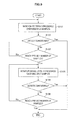
- FIG. 9 is a flowchart illustrating an example of the operation of the digital signal processing device 100 according to one embodiment of the present disclosure.
- FIG. 9 illustrates an example of the processing of the signal coincidence detector 130 contained in the digital signal processing device 100 .
- the signal coincidence detector 130 first monitors the original 1-bit delay signal S A from the delay line 103 and the ⁇ re-modulated 1-bit signal S B from the ⁇ modulator 106 every sampling timing for the pre-set number of samples (Step S 101 ).
- Step S 102 it is judged whether or not the signal coincidence detector 130 detects the pattern coincidence continuing over, for example, four samples.
- the signal coincidence detector 130 When the pattern coincidence continuing over four samples is detected, (Step S 102 , Yes), the signal coincidence detector 130 generates a coincidence detection signal S T which shows that pattern coincidence is detected, supplies the same to the switching controller 129 , and then ends the processing.
- the signal coincidence detector 130 judges whether or not the sample number reaches the pre-set number of samples (Step S 103 ).
- Step S 103 When the sample number does not reach the pre-set number of samples (Step S 103 , No), the signal coincidence detector 130 returns to Step S 101 , and then repeats the processing. On the other hand, when the sample number reaches the pre-set number of samples (Step S 103 , Yes), the signal coincidence detector 130 then monitors the original 1-bit delay signal S A from the delay line 103 and the ⁇ re-modulated 1-bit signal S B from the ⁇ modulator 106 again every sampling timing for the pre-set number of samples in the same section as the section of the target samples from Step S 101 to Step S 103 (Step S 104 ).
- Step S 105 it is judged whether or not the signal coincidence detector 130 detects the signal level coincidence continuing over, for example, four samples.
- Step S 105 Yes
- the signal coincidence detector 130 generates a coincidence detection signal S T which shows that level coincidence is detected, supplies the same to the controller 129 , and then ends the processing.
- Step S 105 No
- the signal coincidence detector 130 judges whether or not the sample number reaches the pre-set number of samples (Step S 106 ).
- Step S 106 When the sample number does not reach the pre-set number of samples (Step S 106 , No), the signal coincidence detector 130 returns to Step S 104 , and then repeats the processing. On the other hand, when the sample number reaches the pre-set number of samples (Step S 106 , Yes), the signal coincidence detector 130 ends the processing.
- the signal coincidence detector 130 first attempts to detect the pattern coincidence between the ⁇ modulated signal S A and the ⁇ re-modulated signal S B over a plurality of samples for the pre-set number of samples.
- the signal coincidence detector 130 generates a coincidence detection signal S T which shows that the pattern coincidence is detected and the switching controller 129 switches between the ⁇ modulated signal S A and the ⁇ re-modulated signal S B according to the coincidence detection signal S T generated by the signal coincidence detector 130 .
- the signal coincidence detector 130 When the coincidence between the ⁇ modulated signal S A and the ⁇ re-modulated signal S B over a plurality of samples may not be detected for the pre-set number of samples, the signal coincidence detector 130 next attempts to detect the level coincidence between the ⁇ modulated signal S A and the ⁇ re-modulated signal S B over a plurality of samples for the pre-set number of samples. When the level coincidence is detected, the signal coincidence detector 130 generates a coincidence detection signal S T which shows that level coincidence is detected and the switching controller 129 switches between the ⁇ modulated signal S A and the ⁇ re-modulated signal S B according to the coincidence detection signal S T generated by the signal coincidence detector 130 .
- the signal coincidence detector 130 attempts to detect coincidence of the 0/1 appearance frequency between the ⁇ modulated signal S A and the ⁇ re-modulated signal S B over a plurality of samples for the pre-set number of samples.
- the signal coincidence detector 130 generates a coincidence detection signal S T which shows that coincidence of the 0/1 of appearance frequency is detected and the switching controller 129 switches between the ⁇ modulated signal S A and the ⁇ re-modulated signal S B according to the coincidence detection signal S T generated by the signal coincidence detector 130 .
- the signal coincidence detector 130 may monitor both the pattern coincidence and the level coincidence between the ⁇ modulated signal S A and the ⁇ re-modulated signal S B over a plurality of samples for the pre-set number of samples. Then, the signal coincidence detector 130 may detect the pattern coincidence or the level coincidence after the end of the monitoring of the pre-set number of samples, and then may generate a coincidence detection signal S T which shows that the pattern coincidence is detected or a coincidence detection signal S T which shows that the level coincidence is detected. It may be configured so that the switching controller 129 switches between the ⁇ modulated signal S A and the ⁇ re-modulated signal S B according to the coincidence detection signal S T generated by the signal coincidence detector 130 .
- This embodiment describes the case where the signal coincidence detector 130 first attempts to detect the pattern coincidence between the ⁇ modulated signal S A and the ⁇ re-modulated signal S B over a plurality of samples for the pre-set number of samples, and then attempts to detect the level coincidence between the ⁇ modulated signal S A and the ⁇ re-modulated signal S B over a plurality of samples for the pre-set number of samples but the present disclosure is not limited to the example.
- the signal coincidence detector 130 may perform the signal coincidence detection in a multistage manner by the use of the feature amount serving as another basis of the signal coincidence.
- the signal coincidence detection is performed in a multistage manner, in the case where there is a necessity of switching between the original ⁇ modulated signal and the ⁇ re-modulated signal in which the original ⁇ modulated signal is subjected to the ⁇ modulation again within the pre-set number of samples (time), the generation of the noises at the changeover point can be reduced with higher probability.
- the digital signal processing device 100 in this embodiment first attempts to detect the pattern coincidence between the ⁇ modulated signal S A and the ⁇ re-modulated signal S B over a plurality of samples for the pre-set number of samples by the signal coincidence detector 130 .
- the signal coincidence detector 130 When the pattern coincidence is detected, the signal coincidence detector 130 generates a coincidence detection signal S T which shows that the pattern coincidence is detected and the switching controller 129 switches between the ⁇ modulated signal S A and the ⁇ re-modulated signal S B according to the coincidence detection signal S T generated by the signal coincidence detector 130 .
- the signal coincidence detector 130 When the coincidence between the ⁇ modulated signal S A and the ⁇ re-modulated signal S B over a plurality of samples may not be detected for the pre-set number of samples, the signal coincidence detector 130 next attempts to detect the level coincidence between the ⁇ modulated signal S A and the ⁇ re-modulated signal S B over a plurality of samples for the pre-set number of samples. When the level coincidence is detected, the signal coincidence detector 130 generates a coincidence detection signal S T which shows that level coincidence is detected and the switching controller 129 switches between the ⁇ modulated signal S A and the ⁇ re-modulated signal S B according to the coincidence detection signal S T generated by the signal coincidence detector 130 .
- the digital signal processing device 100 in this embodiment can more certainly reduce the generation of noises at the changeover point by switching between the ⁇ modulated signal S A and the ⁇ re-modulated signal S B as described above.
- the digital signal apparatus 100 which switches between the ⁇ modulated signal S A and the ⁇ re-modulated signal S B is provided according to one embodiment of the present disclosure.
- the digital signal apparatus 100 When the digital signal apparatus 100 according to one embodiment of the present disclosure switches between the ⁇ modulated signal S A and the ⁇ re-modulated signal S B , the digital signal apparatus 100 first attempts to detect the pattern coincidence between the ⁇ modulated signal S A and the ⁇ re-modulated signal S B over a plurality of samples for the pre-set number of samples. When the pattern coincidence is detected, the digital signal apparatus 100 generates the coincidence detection signal S T which shows that pattern coincidence is detected, and then switches between the ⁇ modulated signal S A and the ⁇ re-modulated signal S B according to the coincidence detection signal S T .
- the digital signal apparatus 100 When the coincidence between the ⁇ modulated signal S A and the ⁇ re-modulated signal S B over a plurality of samples may not be detected for the pre-set number of samples, the digital signal apparatus 100 next attempts to detect the level coincidence between the ⁇ modulated signal S A and the ⁇ re-modulated signal S B over a plurality of samples for the pre-set number of samples. When the level coincidence is detected, the digital signal apparatus 100 generates the coincidence detection signal S T which shows that level coincidence is detected, and then switches between the ⁇ modulated signal S A and the ⁇ re-modulated signal S B according to the coincidence detection signal S T .
- the digital signal processing device 100 in this embodiment can more certainly reduce the generation of noises at the changeover point by switching between the ⁇ modulated signal S A and the ⁇ re-modulated signal S B as described above.
- the generation of noises at the changeover point can be more certainly reduced by switching between the ⁇ modulated signal S A and the ⁇ re-modulated signal S B according to the embodiment of the present disclosure.
- the digital signal processing device 100 is suitable for the use of an apparatus which converts analog signals into digital signals for recording, particularly a recording/reproducing apparatus which records sound, as described above.
- the digital signal processing device 100 is suitable for the use of apparatuses other than the recording/reproducing apparatus insofar as the apparatuses switch between the original ⁇ modulated signal and the ⁇ re-modulated signal to thereby record digital signals.
- Each step in the processing performed by each device of this specification may not be performed in time sequence in accordance with the order shown in the sequence diagram or the flow chart. For example, each step in the processing performed by each device may be processed in order different from the order shown in the flow chart or may be processed in parallel.
- a computer program for causing hardware built in each device, such as CPU, ROM, and RAM, to demonstrate a function equivalent to that in the configuration of each device described above can also be created.
- a storage medium in which the computer program is stored can also be provided.
- a series of processing can also be achieved by hardware by constituting each functional block shown in the functional block diagram with hardware.
- present technology may also be configured as below.
- a signal processing device including:
- a signal coincidence detection portion which detects samples, in which values based on a number of times of appearance of bits coincide with each other over a plurality of samples within a pre-set period, between a first modulated signal obtained by delaying an input signal obtained by ⁇ modulation and a second modulated signal obtained by subjecting the input signal to the ⁇ modulation again;
- a switching control portion which controls the switching between the first modulated signal and the second modulated signal by the signal changeover portion in the samples in which the values based on the number of times of the appearance coincide with each other obtained by the signal coincidence detection portion.
- the signal coincidence detection portion detects a section of samples in which the coincidence of the values based on the number of times of the appearance continues
- switching control portion controls the switching between the first modulated signal and the second modulated signal in the section of the samples.
- the signal coincidence detection portion detects a section of samples in which the values based on the number of times of the appearance continuously coincide with each other with the same value
- switching control portion controls the switching between the first modulated signal and the second modulated signal in the section of the samples.
- switching control portion controls to perform the switching between the first modulated signal and the second modulated signal with any sample other than a first sample and a final sample in the section of the samples.
- the switching control portion controls the switching between the first modulated signal and the second modulated signal in the longest section of the samples.
- the signal coincidence detection portion when the signal coincidence detection portion attempts to detect samples in which patterns of bits over a plurality of samples within the pre-set period coincide with each other and when samples in which the patterns coincide with each other are not present, the signal coincidence detection portion detects samples in which values based on a number of times of appearance of the bits coincide with each other over a plurality of samples within the pre-set period.
- the value based on the number of times of the appearance of the bits over the plurality of samples is a value of a signal level over the plurality of samples.
- the value based on the number of times of the appearance of the bits over the plurality of samples is a number of times of appearance frequency of the bits over the plurality of samples.
- a signal processing method including:
Landscapes
- Engineering & Computer Science (AREA)
- Signal Processing (AREA)
- Physics & Mathematics (AREA)
- Nonlinear Science (AREA)
- Theoretical Computer Science (AREA)
- Compression, Expansion, Code Conversion, And Decoders (AREA)
Abstract
Description
-
- 2.1. Example of configuration of signal processing device
- 2.2. Example of operation of signal processing device
Claims (11)
Applications Claiming Priority (2)
| Application Number | Priority Date | Filing Date | Title |
|---|---|---|---|
| JP2013-237847 | 2013-11-18 | ||
| JP2013237847A JP2015099964A (en) | 2013-11-18 | 2013-11-18 | Signal processing apparatus, signal processing method, and computer program |
Publications (2)
| Publication Number | Publication Date |
|---|---|
| US20150142455A1 US20150142455A1 (en) | 2015-05-21 |
| US9589591B2 true US9589591B2 (en) | 2017-03-07 |
Family
ID=53174191
Family Applications (1)
| Application Number | Title | Priority Date | Filing Date |
|---|---|---|---|
| US14/534,592 Expired - Fee Related US9589591B2 (en) | 2013-11-18 | 2014-11-06 | Signal processing device, signal processing method, and computer program |
Country Status (2)
| Country | Link |
|---|---|
| US (1) | US9589591B2 (en) |
| JP (1) | JP2015099964A (en) |
Families Citing this family (1)
| Publication number | Priority date | Publication date | Assignee | Title |
|---|---|---|---|---|
| JP2015099964A (en) * | 2013-11-18 | 2015-05-28 | ソニー株式会社 | Signal processing apparatus, signal processing method, and computer program |
Citations (7)
| Publication number | Priority date | Publication date | Assignee | Title |
|---|---|---|---|---|
| US5574453A (en) * | 1994-03-03 | 1996-11-12 | Sony Corporation | Digital audio recording apparatus |
| US5793316A (en) * | 1995-12-27 | 1998-08-11 | Sony Corporation | Digital signal processing method and apparatus |
| US6064700A (en) * | 1996-07-26 | 2000-05-16 | Sony Corporation | 1-bit digital signal processing device, recording device, and reproducing device |
| JP3318823B2 (en) | 1995-12-27 | 2002-08-26 | ソニー株式会社 | Digital signal processing apparatus and method |
| US7068196B2 (en) * | 2002-08-09 | 2006-06-27 | Sony Corporation | Digital signal processing device and digital signal processing method |
| US20070241951A1 (en) * | 2006-03-24 | 2007-10-18 | Volker Neubauer | Sigma-delta modulator and method for sigma-delta modulation |
| US20150142455A1 (en) * | 2013-11-18 | 2015-05-21 | Sony Corporation | Signal processing device, signal processing method, and computer program |
-
2013
- 2013-11-18 JP JP2013237847A patent/JP2015099964A/en active Pending
-
2014
- 2014-11-06 US US14/534,592 patent/US9589591B2/en not_active Expired - Fee Related
Patent Citations (7)
| Publication number | Priority date | Publication date | Assignee | Title |
|---|---|---|---|---|
| US5574453A (en) * | 1994-03-03 | 1996-11-12 | Sony Corporation | Digital audio recording apparatus |
| US5793316A (en) * | 1995-12-27 | 1998-08-11 | Sony Corporation | Digital signal processing method and apparatus |
| JP3318823B2 (en) | 1995-12-27 | 2002-08-26 | ソニー株式会社 | Digital signal processing apparatus and method |
| US6064700A (en) * | 1996-07-26 | 2000-05-16 | Sony Corporation | 1-bit digital signal processing device, recording device, and reproducing device |
| US7068196B2 (en) * | 2002-08-09 | 2006-06-27 | Sony Corporation | Digital signal processing device and digital signal processing method |
| US20070241951A1 (en) * | 2006-03-24 | 2007-10-18 | Volker Neubauer | Sigma-delta modulator and method for sigma-delta modulation |
| US20150142455A1 (en) * | 2013-11-18 | 2015-05-21 | Sony Corporation | Signal processing device, signal processing method, and computer program |
Also Published As
| Publication number | Publication date |
|---|---|
| US20150142455A1 (en) | 2015-05-21 |
| JP2015099964A (en) | 2015-05-28 |
Similar Documents
| Publication | Publication Date | Title |
|---|---|---|
| US5701124A (en) | 1-bit signal processing apparatus capable of amplitude modulation and recording or reproducing apparatus having loaded thereon the signal processing apparatus | |
| EP0783207B1 (en) | digital signal processing method and apparatus | |
| WO2016199596A1 (en) | Signal processing device, signal processing method, and program | |
| JP3334413B2 (en) | Digital signal processing method and apparatus | |
| US9589591B2 (en) | Signal processing device, signal processing method, and computer program | |
| US5793316A (en) | Digital signal processing method and apparatus | |
| US20020121999A1 (en) | Digital signal processing apparatus and method | |
| US9742381B2 (en) | Pulse width modulator and non-transitory computer readable medium for storing program for pulse width modulator | |
| US7068196B2 (en) | Digital signal processing device and digital signal processing method | |
| US7154419B2 (en) | Audio apparatus for processing voice and audio signals | |
| US20200051576A1 (en) | Signal processing apparatus, signal processing method, and program | |
| JP3826813B2 (en) | Digital signal processing apparatus and digital signal processing method | |
| JP3339315B2 (en) | Digital signal processing device, recording device and reproducing device | |
| US8878710B2 (en) | Low latency filter | |
| US8368569B2 (en) | Data converting device, program and method | |
| EP3691130A1 (en) | Re-quantization device having noise shaping function, signal compression device having noise shaping function, and signal transmission device having noise shaping function | |
| KR100496669B1 (en) | Digital signal processing method and apparatus | |
| JP3821151B2 (en) | 1-bit audio signal generating apparatus and 1-bit audio signal generating method | |
| JP2008046405A (en) | Encoding method and decoding method in adaptive differential pulse code modulation system | |
| JP2000114971A (en) | Digital signal generator | |
| JP5474145B2 (en) | Fade processing device for DSD signal in audio products | |
| JP3821150B2 (en) | Digital signal processing apparatus and digital signal processing method | |
| JP3807599B2 (en) | Recording device | |
| JP2003032110A (en) | Analog to digital converting method | |
| JP2007074113A (en) | Delta-sigma modulation circuit and switching amplifier having the same |
Legal Events
| Date | Code | Title | Description |
|---|---|---|---|
| AS | Assignment |
Owner name: SONY CORPORATION, JAPAN Free format text: ASSIGNMENT OF ASSIGNORS INTEREST;ASSIGNORS:MATSUMURA, YUUKI;SUZUKI, SHIRO;REEL/FRAME:034179/0672 Effective date: 20141007 |
|
| FEPP | Fee payment procedure |
Free format text: PAYOR NUMBER ASSIGNED (ORIGINAL EVENT CODE: ASPN); ENTITY STATUS OF PATENT OWNER: LARGE ENTITY |
|
| STCF | Information on status: patent grant |
Free format text: PATENTED CASE |
|
| MAFP | Maintenance fee payment |
Free format text: PAYMENT OF MAINTENANCE FEE, 4TH YEAR, LARGE ENTITY (ORIGINAL EVENT CODE: M1551); ENTITY STATUS OF PATENT OWNER: LARGE ENTITY Year of fee payment: 4 |
|
| FEPP | Fee payment procedure |
Free format text: MAINTENANCE FEE REMINDER MAILED (ORIGINAL EVENT CODE: REM.); ENTITY STATUS OF PATENT OWNER: LARGE ENTITY |
|
| LAPS | Lapse for failure to pay maintenance fees |
Free format text: PATENT EXPIRED FOR FAILURE TO PAY MAINTENANCE FEES (ORIGINAL EVENT CODE: EXP.); ENTITY STATUS OF PATENT OWNER: LARGE ENTITY |
|
| STCH | Information on status: patent discontinuation |
Free format text: PATENT EXPIRED DUE TO NONPAYMENT OF MAINTENANCE FEES UNDER 37 CFR 1.362 |
|
| FP | Lapsed due to failure to pay maintenance fee |
Effective date: 20250307 |