EP0776125A2 - Vorrichtung zur Korrektur von Kissenverzerrungen - Google Patents
Vorrichtung zur Korrektur von Kissenverzerrungen Download PDFInfo
- Publication number
- EP0776125A2 EP0776125A2 EP96118472A EP96118472A EP0776125A2 EP 0776125 A2 EP0776125 A2 EP 0776125A2 EP 96118472 A EP96118472 A EP 96118472A EP 96118472 A EP96118472 A EP 96118472A EP 0776125 A2 EP0776125 A2 EP 0776125A2
- Authority
- EP
- European Patent Office
- Prior art keywords
- reactor
- coil
- horizontal
- vertical
- picture
- Prior art date
- Legal status (The legal status is an assumption and is not a legal conclusion. Google has not performed a legal analysis and makes no representation as to the accuracy of the status listed.)
- Granted
Links
- 240000000136 Scabiosa atropurpurea Species 0.000 title 1
- 241000226585 Antennaria plantaginifolia Species 0.000 claims description 26
- 230000007423 decrease Effects 0.000 claims description 20
- 239000003990 capacitor Substances 0.000 claims description 14
- 238000010586 diagram Methods 0.000 description 13
- 238000010894 electron beam technology Methods 0.000 description 7
- 230000000694 effects Effects 0.000 description 4
- 230000003247 decreasing effect Effects 0.000 description 3
- 229920006395 saturated elastomer Polymers 0.000 description 3
- 230000004075 alteration Effects 0.000 description 2
- 238000000034 method Methods 0.000 description 2
- 238000012986 modification Methods 0.000 description 2
- 230000004048 modification Effects 0.000 description 2
- 238000013459 approach Methods 0.000 description 1
- 239000002131 composite material Substances 0.000 description 1
- 230000001419 dependent effect Effects 0.000 description 1
- 238000006073 displacement reaction Methods 0.000 description 1
- 238000004519 manufacturing process Methods 0.000 description 1
- 230000002093 peripheral effect Effects 0.000 description 1
Images


Classifications
-
- H—ELECTRICITY
- H04—ELECTRIC COMMUNICATION TECHNIQUE
- H04N—PICTORIAL COMMUNICATION, e.g. TELEVISION
- H04N3/00—Scanning details of television systems; Combination thereof with generation of supply voltages
- H04N3/10—Scanning details of television systems; Combination thereof with generation of supply voltages by means not exclusively optical-mechanical
- H04N3/16—Scanning details of television systems; Combination thereof with generation of supply voltages by means not exclusively optical-mechanical by deflecting electron beam in cathode-ray tube, e.g. scanning corrections
- H04N3/22—Circuits for controlling dimensions, shape or centering of picture on screen
- H04N3/23—Distortion correction, e.g. for pincushion distortion correction, S-correction
- H04N3/237—Distortion correction, e.g. for pincushion distortion correction, S-correction using passive elements, e.g. diodes
Definitions
- the present invention relates to a correction apparatus and a correction technique for correcting inner pincushion distortion in the vertical direction of a cathode ray tube (CRT) display apparatus which is suitable for a display apparatus of a computer corresponding to a multiscanning system, or the like.
- CTR cathode ray tube
- a picture made by projection on a front screen of a CRT by deflecting electron beams mainly includes distortion of pincushion shape.
- various circuits such as a "correction circuit of upper and lower horizontal-line-distortion” or a “correction circuit of vertical line distortion” are widely used in conventional arts.
- further distortion arises in the picture corrected by these correction circuits, for example in a central part of a vertical line.
- this distortion which arises on a vertical line of the picture is called “inner pincushion distortion in vertical direction”.
- the front screen of the CRT has a spherical face having its center coinciding with the deflection center of the electron beam, positional change of a luminescent spot from center point on the front screen is proportional to change of a deflection current.
- An actual front screen of the CRT is similar to a flat face.
- a deflection angle and a time are represented by ⁇ and t, respectively
- a displacement amount X(t) of the luminescent spot on the flat screen is proportional to tan ⁇ . Therefore, picture distortion called "S-distortion" arises. In the S-distortion, an amount of horizontal deflection gradually increases toward end parts of a picture face of the CRT.
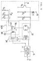
- FIG. 14 is a horizontal deflection circuit including an S-distortion correction circuit which is generally used in the conventional art to correct the S-distortion.
- a pulse signal of a horizontal scanning period (hereafter is referred to as horizontal period) is applied to the base of a horizontal output transistor Q 1 , and a sawtooth current of the horizontal period (horizontal deflection current) passes through a horizontal deflection coil 11.
- An S-distortion correction capacitor C S is connected in series with the horizontal deflection coil 11, and a voltage of parabolic waveform is generated on the S-distortion correction capacitor C S by the sawtooth current.
- a horizontal deflection current of sawtooth waveform is modulated to a S-shaped current by the voltage of parabolic waveform, and increase of an amount of horizontal deflection is suppressed in right and left end parts of the picture face.
- the above-mentioned method is widely used.
- FIG. 2A is a waveform diagram of a general parabolic waveform voltage e S (t)
- FIG. 2B is a waveform diagram of a general horizontal deflection current I y (t).
- a required correction amount of the S-distortion which arises in an actual CRT display apparatus is in inverse proportion to a distance from the deflection center of the CRT to a position on the picture face, and therefore, varies dependent on the position on the picture face. For example, on a CRT screen having a large curvature radius, since an upper part and a lower part of the CRT screen are far from the deflection center in comparison with a central part, the required correction amount of the S-distortion is smaller than that in the central part.
- the above-mentioned point is not taken into account in the conventional S-distortion correction circuit.
- An object of the present invention is to provide the picture distortion correction apparatus of which a correction amount of S-distortion in an upper and a lower parts of a picture face is different from that in a central part, and a suitable S-distortion correction is realized in overall picture face of a front screen having a large curvature radius.
- the picture distortion correction apparatus of a first mode of the present invention comprises a saturable reactor, and an inductance of the saturable reactor passing a horizontal deflection current is controlled corresponding to a vertical deflection current.
- the picture distortion correction apparatus of a second mode of the present invention comprises a saturable reactor having a first, a second, a third and a fourth reactor coils which are wound on a core, connected in series with each other, and connected in series with a horizontal deflection coil to enable passing a horizontal deflection current through these reactor coils,
- the picture distortion correction apparatus of a third mode of the present invention comprises one or two saturable reactors to be connected to each other,
- the inductance of the saturable reactor is controlled depending on the vertical deflection current, a correction amount of the S-distortion in the horizontal deflection can be varied corresponding to the amount of the vertical deflection.
- the correction amount of the S-distortion of the horizontal deflection can be selected to a suitable value, and an inner pincushion distortion in the vertical direction can be corrected.
- the inductance of the saturable reactor connected in series with the horizontal deflection coil is varied in the vertical scanning period (hereinafter is referred to as vertical period) and the horizontal scanning period (hereinafter is refereed to as horizontal period). Consequently, the correction amount of the S-distortion is controlled in the vertical period, and horizontal linearity of the horizontal deflection current is controlled by varying the inductance in the horizontal period, and an amount of the control is further varied in the vertical period. Consequently, the inner pincushion distortion in the vertical direction is corrected.
- a total inductance of the first to fourth reactor coils increases in the central part in the horizontal direction in the use of deflection to the upper part and the lower part of the picture face, decreases in the central part and increases toward both end parts in the horizontal direction in the case of deflection in the center part of the vertical direction of the picture face, and increases in both end parts and decreases in the central part in the vertical scanning period. Consequently, the signal of the S-distortion correction can be modulated in the vertical period.
- a correction amount of horizontal linearlity in the central part and a peripheral part of the picture face by variation of the total inductance of the saturable reactor in the horizontal scanning period can be changed in the vertical scanning period. Consequently, the inner pincushion distortion in the vertical direction can be corrected without giving harmful influence to other part of the picture.
- the inductance of the saturable reactor is decreased in the central period of the horizontal period, and the inductance is increased in the period of both end parts of the horizontal period, and the amplitude of the horizontal deflection current is extended in the central part and reduced in the periods of both right and left end parts in the vertical scanning. Consequently, the inner pincushion distortion in the vertical direction is improved.
- FIG. 1 to FIG. 10 A first embodiment of the present invention is described hereafter with reference to FIG. 1 to FIG. 10.
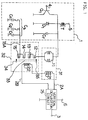
- FIG. 1 is a circuit diagram of a deflection circuit for deflecting an electron beam comprising a saturable reactor of the first embodiment of the present invention.
- the deflection circuit comprises a horizontal deflection circuit 1 including a S-distortion correction capacitor C S , a vertical deflection circuit 25, a deflection yoke 31 receiving outputs of the horizontal deflection circuit 1 and the vertical deflection circuit 25 and a saturable reactor unit 32 for correcting "inner pincushion distortion in the vertical direction".
- a terminal 5 to be coupled to a power source is connected through a choke coil T to the collector of a horizontal output transistor Q 1 , the cathode of a diode D 1 , a horizontal resonance capacitor C r and one end of a horizontal deflection coil 11 of the deflection yoke 31.
- the other end of the horizontal deflection coil 11 is connected to one end of a first reactor coil 12 of the saturable reactor unit 32.
- a second reactor coil 13, a third reactor coil 14 and a fourth reactor coil 15 are connected in series with the first reactor coil 12 in the named order, and a terminal 15A of the fourth reactor coil 15 is connected to an S-distortion correction capacitor C S .
- a terminal 6 is connected to a power source (not shown), and a terminal 3 is connected to a vertical deflection driving circuit (not shown).
- a serially-coupled pair of a vertical deflection coil 21 of the vertical deflection yoke 31 and a fifth coil 22 of the saturable reactor unit 32 is connected across output terminals 2A and 2B of the vertical deflection circuit 25.
- the horizontal deflection circuit 1 generates a sawtooth current of a horizontal scanning period (hereinafter is referred to as horizontal period), and causes the horizontal deflection current to flow in the horizontal deflection coil 11 of the deflection yoke 31.
- the vertical deflection circuit 25 generates a sawtooth current of a vertical scanning period (hereinafter is referred to as vertical period), and causes the vertical deflection current to flow to the vertical deflection coli 21 of the deflection yoke 31.
- the first reactor coil 12 and the second reactor coil 13 are connected in series in inverse polarity with each other so that waveform change of the reactor coil 12 caused by change of the horizontal deflection current is in inverse polarity to waveform change of the reactor coil 13 caused by the change of the horizontal deflection current, so that changes of inductances of the reactor coils 12 and 13 are each-other opposite. For example, when the inductance of the reactor coil 12 decreases by change of the horizontal deflection current, the inductance of the reactor coil 13 increases.
- the third reactor coil 14 and the fourth reactor coil 15 are also similarly connected in series in inverse polarity with each other so that the waveform change of the reactor coil 14 caused by change of the horizontal deflection current is in inverse polarity to the waveform change of the reactor coil 15 caused by the change of the horizontal deflection current.
- FIG. 4 is described in detail later.
- a constant magnetic bias is applied to the first to fourth reactor coils 12 --- 15 by permanent magnets 34 and 35. Therefore, magnetically saturated states of the first to fourth reactor coils 12 --- 15 are controlled on the basis of change of the waveform of the vertical deflection current passing in the coil 22 which is magnetically coupled to the first to fourth reactor coils 12 --- 15.
- the first and second reactor coils 12 and 13 have characteristics such that the total inductance (L 1 + L 2 ) of the inductance L 1 and the inductance L 2 , shown by a curve 41, increases at a part corresponding to an upper part of the picture face, and decreases at a part corresponding to a lower part thereof.
- the third reactor coil 14 and the fourth reactor coil 15 have characteristics such that a curve 42 representing the total inductance (L 3 + L 4 ) of the inductance L 3 and the inductance L 4 is symmetrical to the curve 41 with respect to the line V L representing zero of the vertical deflection current.
- the total inductance L S which is the sum of the inductances of the first to fourth reactor coils 12 --- 15 shown by a curve 43 in FIG. 4 increases toward an upper end and a lower end of the picture face of vertical deflection, and decreases in the center part.
- the S-distortion correction amount (which is amount of known correction current to be added to the horizontal deflection current so as to correct the S-direction) is modulated.
- the S-distortion has been corrected by modulating the horizontal deflection current of the sawtooth waveform in a stretched S-shape manner by using a parabolic waveform voltage e S (t) generated at the S-distortion correction capacitor C S .
- the parabolic waveform voltage e S (t) generated at the S-distortion correction capacitor C S is shown in FIG. 2A.
- the waveform of the horizontal deflection current I y (H, t) modulated by the parabolic waveform voltage e S (t) is shown in FIG. 2B.
- FIG. 3 is an equivalent circuit of the horizontal deflection circuit 1, the vertical deflection circuit 25, the saturable reactor unit 32 and the horizontal defection coil 11 in FIG. 1.
- a power supply voltage applied to the terminal 5 in FIG. 1 is represented by E b .
- the horizontal output transistor Q 1 which is operated by a pulse signal of the horizontal period applied to a terminal 4 and a damper diode D 1 are represented by SW.
- a horizontal resonance capacitor is represented by C r .
- a capacitance of the S-distortion correction capacitor C S is represented by CS, and an inductance of the horizontal deflection coil 11 is represented by L y .
- the total inductance (L 1 + L 2 + L 3 + L 4 ) is represented by L S .
- the total inductance L S is varied by modulation in the vertical period.
- the S-distortion correction amount of the horizontal deflection current I y (H) is varied by variation of the total inductance L S in the vertical period.
- the variation of the S-distortion correction amount is described.
- a voltage across both terminals of the S-distortion correction capacitor C S becomes a waveform shown in FIG. 2A by superimposing the parabolic waveform voltage e S (t).
- the horizontal deflection current I y (H) passing through the horizontal deflection coil 11 is varied by the parabolic waveform voltage e S (t) as shown by FIG. 2B.
- both right end part and left end part of a picture tend to extend, and the central part of the picture tends to shrink in the horizontal direction, in comparison with the central part in the vertical direction of the picture face. Therefore, overcorrection of the S-distortion in the upper and lower parts of the picture face is improved, and as a result, the inner pincushion distortion in the vertical direction is improved.
- the core 33 having two windows 33A and 33B is provided with two permanent magnets 34 and 35 for producing fixed magnetic field.
- the first reactor coil 12 and the second reactor coil 13 are wound through the window 33A of the core 33.
- the third reactor coil 14 and the fourth reactor coil 15 are wound through the window 33B.
- the fifth coil 22 is wound around the whole core 33 at the central part.
- the reactor coils 12 --- 15 and the coil 22 are shown by respective cross-sections.
- the fifth coil 22 produces magnetic field which is varied by the vertical deflection current in the vertical scanning period.
- Two permanent magnets 34 and 35 are arranged symmetrically with respect to the center axis of the center leg 33D between two windows 33A and 33B of the core 33 at both ends of the core 33, respectively.
- the permanent magnets 34 and 35 are attached to the core 33 in such direction that respective magnetic lines are directed to central parts 33C of the core 33, and the magnetic fields produced by the permanent magnets 34 and 35 are cancelled in the core 33 except the central parts 33C of a circumferential part of the core 33.
- the magnetic fields in the reactor coils 12, 13, 14 and 15 are different from each other depending on respective values and polarities of currents passing through the reactor coils 12 --- 15.
- magnetic field produced by the coil 22 is varied by a current passing through the coil 22, but the magnetic fields produced by the permanent magnets 34 and 35 do not change.
- FIG. 6 shows state of magnetic field produced in the core 33 when the maximum vertical deflection current I y (V) passes through the coil 22 of the saturable reactor 32.
- the configuration of the saturable reactor 32 is identical with that in FIG. 5.
- FIG. 6 shows the state where the horizontal deflection current I y (H) to be passed through the reactor coils 12 --- 15 is zero. In this state, the electron beam is deflected to the upper part of the picture face, and magnetic fields produced by the coil 22 are shown by broken-line-arrows ⁇ V (hereinafter is referred to as magnetic fields ⁇ V ).
- Magnetic fields in the parts 12A and 13A of the core 33 surrounded by the respective reactor coils 12 and 13 becomes values represented by ⁇ S1 - ⁇ V each of which is a difference between magnetic field ⁇ S1 and the magnetic field ⁇ V . Therefore, the magnetic fields in the parts 12A and 13A decrease, and the sum of the inductances L 1 and L 2 increases at a hill portion 41A of the curve 41 shown in FIG. 4.
- magnetic fields in the parts 14A and 15A of the core 33 surrounded by the respective reactor coils 14 and 15 are the sum of magnetic fields ⁇ S2 and ⁇ V . Therefore, the magnetic fields in the parts 14A and 15A increase, and the sum of the inductances L 3 and L 4 decreases to a flat portion 42B of the curve 42 shown in FIG. 4.
- the total inductance L S becomes a valley-like characteristic lowered in the central part in the vertical period as shown by the curve 43 in FIG. 4, and the above-mentioned characteristic of the S-distortion correction can be improved.
- FIG. 7 shows state of magnetic field of the core 33 when the maximum vertical deflection current I y (V) passes through the coil 22, and the maximum horizontal deflection current I y (H) passes through the reactor coils 12 --- 15.
- the electron beam is deflected upward of the picture face by the vertical deflection current I y (V) passing through the coil 22, and the magnetic fields ⁇ V are produced in the core 33.
- Magnetic field produced by the reactor coil 12 is represented by arrow ⁇ H1
- magnetic field produced by the reactor coil 13 is represented by arrow ⁇ H2 .
- Magnetic field produced by the reactor coil 14 is represented by arrow ⁇ H3
- magnetic field produced by the reactor coil 15 is represented by arrow ⁇ H4 .
- arrows ⁇ H1 , ⁇ H2 , ⁇ H3 and ⁇ H4 designates directions of magnetic fields ⁇ H1 , ⁇ H2 , ⁇ H3 and ⁇ H4 , respectively.
- each absolute value of the magnetic fields ⁇ S1 and ⁇ S2 produced by the permanent magnets 34 and 35 is represented by ⁇ Sn .
- Relation among the absolute values ⁇ Hn , ⁇ Sn and ⁇ V is selected to as follows: ⁇ Hn ⁇ ⁇ V ⁇ ⁇ Sn .
- the magnetic field in the part 12A of the core 33 having the coil 12 is represented by ⁇ S1 - ⁇ V - ⁇ H1 .
- the inductance L 1 of the reactor coil 12 slightly increases, while variation of the magnetic field ⁇ ⁇ V + ⁇ H1 is small, because the sum of the magnetic fields ⁇ V and ⁇ H1 ( ⁇ V + ⁇ H1 ) approaches the magnetic field ⁇ S1 .
- the magnetic field is represented by ⁇ S1 - ⁇ V + ⁇ H2 , and therefore, the inductance L 2 is small.
- the magnetic fields ⁇ H3 and ⁇ H4 are varied, the sum of the respective inductances L 3 and L 4 of the reactor coils 14 and 15 is kept to a small value, and therefore can be disregarded in the operation. The reason is that the magnetic saturation is produced by the sum ( ⁇ S2 + ⁇ V ) of the magnetic field ⁇ S2 and ⁇ V .
- FIG. 8 is a diagram showing variation of inductances in a horizontal scanning period when an upper part of the picture face is scanned.
- the inductance L 1 of the reactor coil 12 is shown by a curve 44
- the inductance L 2 of the reactor coil 13 is shown by a curve 45
- the total inductance L S (L 1 + L 2 +L 3 + L 4 ) is shown by a curve 46, since the inductance L 3 + L 4 are negligibly small.
- the inductance L 1 of FIG. 8 is replaced with the inductance L 4 in the curve 44
- the inductance L 2 of FIG. 8 is replaced with the inductance L 3 in the curve 45
- the curve 46 will represents characteristic of inductance in scanning of a lower part of the picture face.
- FIG. 9 shows state of magnetic field of the core 33 in scanning of a leftward part of the picture face (vertical deflection angle is zero).
- the state of the magnetic field is elucidated comparing with the scanning state in the central part of the picture face shown in FIG. 5.
- the magnetic field in the part 12A of the core 33 having the reactor coil 12 is represented by the difference ( ⁇ S1 - ⁇ H1 )between the magnetic fields ⁇ S1 and ⁇ H1 , and therefore the inductance L 1 is large.
- the magnetic field in the part 15A of the core 33 having the reactor coil 15 is represented by the difference ( ⁇ S2 - ⁇ H4 ) between the magnetic fields ⁇ S2 and ⁇ H4 , and therefore, the inductance L 4 is large.
- the variation of the total inductance L S in the vertical scanning period induces a slight horizontal amplitude variation in overall picture face
- the induced variation serves to reduce known side pincushion distortion (not disclosed in the above), which is generally produced at end parts of the picture face.
- the amount of correction described above is one tenth or below of an amount of correction of the side pincushion distortion, and therefore, the S-distortion correction in the present embodiment does not give harmful influence to other picture distortions.
- the first to fourth reactor coils 12 --- 15 and the fifth coil 22 of the saturable reactor 32 are connected in series with the horizontal deflection coil 11 and the vertical deflection coil 21 of the deflection yoke 31, respectively, and therefore, no other connection than the above connections is necessary. Therefore, the picture distortion correction apparatus of the first embodiment can be easily incorporated into a conventional deflection circuit.
- FIG. 11 is a cross-sectional view of a saturable reactor 32A in the second embodiment.
- a single permanent magnet 37 which produces fixed magnetic field is attached to a rectangular core 36 having a single window 36A.
- a first reactor coil 16 and a second reactor coil 17 are wound through the window 36A of the core 36.
- the first reactor coil 16 is connected in series with the second reactor coil 17 in a manner of inverse polarity.
- Respective inductances of the reactor coils 16 and 17 are varied by magnetic fields passing through respective parts of the core 36 surrounded by the reactor 16 and 17.
- a third coil 23 is wound on the circumference of an end part of the core 36.
- the reactor coils 16 and 17 and the coil 23 are shown by the respective cross-sections.
- the vertical deflection current I y (V) of saw-tooth waveform in the vertical deflection period flows in through the third coil 23.
- the saturable reactor 32A in this second embodiment has configuration that the saturable reactor 32 in the first embodiment shown in FIG. 5 is divided into two parts along a central vertical line, and is designed so that the operation and characteristic are substantially similar to those of the saturable reactor 32.
- FIG. 12 is an embodiment of a picture distortion correction apparatus using two saturable reactors 32A shown in FIG. 11.
- the coil 23 of the lower saturable reactor 32A is connected in series with the coil 23 of the upper saturable reactor 32A in a manner of inverse polarity. Consequently, operation and effect of the second embodiment is substantially identical with that of the first embodiment.
- the configuration of the saturable reactor is simplified.
- the vertical deflection current I y (V) passes through two coils 23, and Therefore, load of the vertical deflection circuit 25 increases.
- FIG. 13 is a circuit diagram of a picture distortion correction apparatus using one saturable reactor 32A shown in FIG. 11.
- the saturable reactor 32A serves as the substantially same operation as the saturable reactors shown in FIG. 1 and FIG. 12 by passing a current of parabolic waveform of the vertical period through the third coil 23.
- a bridge circuit 24 of diodes connected to the coil 23 is a well known circuit wherein the vertical deflection current of the saw-tooth waveform is rectified and the current of parabolic waveform is generated.
- Other circuit which passes the current of parabolic waveform of the vertical period through the coil 23 can be used as replacement for the bridge circuit 24.
- Basic operation of the picture distortion correction apparatus shown in FIG. 13 is substantially identical with that of FIG. 12.
- the first and second reactor coils 16 and 17 and the third coil 23 of the saturable reactor 32A are connected in series with the horizontal deflection coil 11 and the vertical deflection coil 21 of the deflection yoke 31, respectively, and therefore similarly to the first embodiment no other connection than the above connections is necessary. Therefore, the picture distortion correction circuit of the second embodiment can be easily incorporated into the conventional deflection circuit. Moreover, the configuration of the saturable reactor 32A is simplified, and therefore easily fabricated, and a fabrication cost is reduced.
Landscapes
- Engineering & Computer Science (AREA)
- Multimedia (AREA)
- Signal Processing (AREA)
- Details Of Television Scanning (AREA)
Priority Applications (1)
| Application Number | Priority Date | Filing Date | Title |
|---|---|---|---|
| EP02026020A EP1301029A3 (de) | 1995-11-21 | 1996-11-18 | Vorrichtung zur Korrektur von Kissenverzerrungen |
Applications Claiming Priority (3)
| Application Number | Priority Date | Filing Date | Title |
|---|---|---|---|
| JP30309995 | 1995-11-21 | ||
| JP07303099A JP3137574B2 (ja) | 1995-11-21 | 1995-11-21 | 画像歪補正装置 |
| JP303099/95 | 1995-11-21 |
Related Child Applications (1)
| Application Number | Title | Priority Date | Filing Date |
|---|---|---|---|
| EP02026020A Division EP1301029A3 (de) | 1995-11-21 | 1996-11-18 | Vorrichtung zur Korrektur von Kissenverzerrungen |
Publications (3)
| Publication Number | Publication Date |
|---|---|
| EP0776125A2 true EP0776125A2 (de) | 1997-05-28 |
| EP0776125A3 EP0776125A3 (de) | 1999-10-06 |
| EP0776125B1 EP0776125B1 (de) | 2003-03-12 |
Family
ID=17916885
Family Applications (2)
| Application Number | Title | Priority Date | Filing Date |
|---|---|---|---|
| EP96118472A Expired - Lifetime EP0776125B1 (de) | 1995-11-21 | 1996-11-18 | Vorrichtung zur Korrektur von Kissenverzerrungen |
| EP02026020A Withdrawn EP1301029A3 (de) | 1995-11-21 | 1996-11-18 | Vorrichtung zur Korrektur von Kissenverzerrungen |
Family Applications After (1)
| Application Number | Title | Priority Date | Filing Date |
|---|---|---|---|
| EP02026020A Withdrawn EP1301029A3 (de) | 1995-11-21 | 1996-11-18 | Vorrichtung zur Korrektur von Kissenverzerrungen |
Country Status (7)
| Country | Link |
|---|---|
| US (1) | US5804928A (de) |
| EP (2) | EP0776125B1 (de) |
| JP (1) | JP3137574B2 (de) |
| KR (1) | KR100262904B1 (de) |
| CN (2) | CN1218558C (de) |
| DE (1) | DE69626606T2 (de) |
| TW (1) | TW310414B (de) |
Cited By (4)
| Publication number | Priority date | Publication date | Assignee | Title |
|---|---|---|---|---|
| WO2003053044A1 (en) * | 2001-12-19 | 2003-06-26 | Thomson Licensing S.A. | Image-geometry corrector for a cathode-ray tube |
| EP1069763A3 (de) * | 1999-07-12 | 2003-10-08 | Matsushita Electric Industrial Co., Ltd. | Ablenkung-Korrekturschaltung für Farbbildröhre |
| EP1056112A3 (de) * | 1999-05-24 | 2003-12-17 | Matsushita Electric Industrial Co., Ltd. | Farbbildröhre |
| CN101557259B (zh) * | 2008-04-10 | 2012-03-07 | 中国科学院西安光学精密机械研究所 | 一种长帧结构光数据包全光速率提升系统 |
Families Citing this family (10)
| Publication number | Priority date | Publication date | Assignee | Title |
|---|---|---|---|---|
| US6013989A (en) * | 1996-05-20 | 2000-01-11 | Samsung Electronics Co., Ltd. | Wide-band horizontal linearity correction circuit |
| JPH11261839A (ja) | 1998-03-13 | 1999-09-24 | Sony Corp | 画歪補正装置 |
| KR100371452B1 (ko) * | 1999-03-31 | 2003-02-06 | 가부시끼가이샤 도시바 | 음극선관장치 |
| TW480525B (en) | 1999-12-22 | 2002-03-21 | Matsushita Electronics Corp | Color display tube device |
| JP2001320601A (ja) | 2000-05-08 | 2001-11-16 | Mitsubishi Electric Corp | 画像歪補正装置 |
| JP2001320600A (ja) | 2000-05-08 | 2001-11-16 | Mitsubishi Electric Corp | 画像歪補正回路 |
| EP1296349A3 (de) | 2001-09-19 | 2005-02-02 | Matsushita Electric Industrial Co., Ltd. | Ablenkjoch |
| CN100553288C (zh) * | 2005-12-06 | 2009-10-21 | 海尔集团公司 | 一种消除彩色电视机枕形失真的电路 |
| US9148571B2 (en) | 2012-09-14 | 2015-09-29 | Apple Inc. | Image distortion correction in scaling circuit |
| JP6305293B2 (ja) * | 2014-09-17 | 2018-04-04 | 株式会社豊田中央研究所 | 磁気結合リアクトル及び電力変換装置 |
Family Cites Families (9)
| Publication number | Priority date | Publication date | Assignee | Title |
|---|---|---|---|---|
| US3681725A (en) * | 1969-08-25 | 1972-08-01 | Denki Onkyo Co Ltd | Saturable reactor for correcting raster distortion |
| JPS4895521U (de) * | 1972-02-17 | 1973-11-14 | ||
| US4084115A (en) * | 1977-02-14 | 1978-04-11 | Rca Corporation | Circuit for correcting setup error in a color television receiver |
| US4321511A (en) * | 1980-08-04 | 1982-03-23 | Rca Corporation | Linearity corrected deflection circuit |
| GB8408694D0 (en) * | 1984-04-04 | 1984-05-16 | Rca Corp | Dynamic "s" correction |
| US4642530A (en) * | 1985-05-10 | 1987-02-10 | Rca Corporation | Raster distortion correction circuit |
| JPH079786B2 (ja) * | 1989-10-06 | 1995-02-01 | 東京特殊電線株式会社 | 偏向ヨークおよび偏向装置およびモノクロームcrt表示装置 |
| JP2561541B2 (ja) * | 1989-12-11 | 1996-12-11 | 三菱電機株式会社 | ラスタ歪補正回路 |
| JPH0746428A (ja) * | 1993-07-23 | 1995-02-14 | Sony Corp | リニアリティー補正回路 |
-
1995
- 1995-11-21 JP JP07303099A patent/JP3137574B2/ja not_active Expired - Fee Related
-
1996
- 1996-11-18 EP EP96118472A patent/EP0776125B1/de not_active Expired - Lifetime
- 1996-11-18 EP EP02026020A patent/EP1301029A3/de not_active Withdrawn
- 1996-11-18 DE DE69626606T patent/DE69626606T2/de not_active Expired - Fee Related
- 1996-11-19 TW TW085114194A patent/TW310414B/zh active
- 1996-11-20 US US08/754,770 patent/US5804928A/en not_active Expired - Fee Related
- 1996-11-21 KR KR1019960056019A patent/KR100262904B1/ko not_active Expired - Fee Related
- 1996-11-21 CN CN031009840A patent/CN1218558C/zh not_active Expired - Fee Related
- 1996-11-21 CN CN96121768A patent/CN1131632C/zh not_active Expired - Fee Related
Non-Patent Citations (1)
| Title |
|---|
| None |
Cited By (6)
| Publication number | Priority date | Publication date | Assignee | Title |
|---|---|---|---|---|
| EP1056112A3 (de) * | 1999-05-24 | 2003-12-17 | Matsushita Electric Industrial Co., Ltd. | Farbbildröhre |
| US6984929B1 (en) | 1999-05-24 | 2006-01-10 | Matsushita Electric Industrial Co., Ltd. | Color picture tube apparatus with pincushion distortion correction |
| EP1069763A3 (de) * | 1999-07-12 | 2003-10-08 | Matsushita Electric Industrial Co., Ltd. | Ablenkung-Korrekturschaltung für Farbbildröhre |
| WO2003053044A1 (en) * | 2001-12-19 | 2003-06-26 | Thomson Licensing S.A. | Image-geometry corrector for a cathode-ray tube |
| FR2844633A1 (fr) * | 2001-12-19 | 2004-03-19 | Thomson Licensing Sa | Correcteur de la geometrie d'image pour tube a rayons cathodiques |
| CN101557259B (zh) * | 2008-04-10 | 2012-03-07 | 中国科学院西安光学精密机械研究所 | 一种长帧结构光数据包全光速率提升系统 |
Also Published As
| Publication number | Publication date |
|---|---|
| JPH09149283A (ja) | 1997-06-06 |
| CN1159117A (zh) | 1997-09-10 |
| DE69626606T2 (de) | 2003-11-06 |
| CN1131632C (zh) | 2003-12-17 |
| EP0776125B1 (de) | 2003-03-12 |
| KR100262904B1 (ko) | 2000-08-01 |
| EP1301029A2 (de) | 2003-04-09 |
| DE69626606D1 (de) | 2003-04-17 |
| CN1474592A (zh) | 2004-02-11 |
| CN1218558C (zh) | 2005-09-07 |
| KR970031791A (ko) | 1997-06-26 |
| US5804928A (en) | 1998-09-08 |
| JP3137574B2 (ja) | 2001-02-26 |
| EP0776125A3 (de) | 1999-10-06 |
| TW310414B (de) | 1997-07-11 |
| EP1301029A3 (de) | 2007-05-09 |
Similar Documents
| Publication | Publication Date | Title |
|---|---|---|
| US5804928A (en) | Picture distortion correction apparatus | |
| EP0201336A2 (de) | Schaltung zur Korrektur von Rasterverzerrungen | |
| US6265836B1 (en) | Image distortion compensating apparatus | |
| EP0689347A1 (de) | Schaltung zur Modulation der Abtastgeschwindigkeit | |
| US5350980A (en) | Nonlinear inductor with magnetic field reduction | |
| JPH05244448A (ja) | 動集束回路 | |
| JPH06233149A (ja) | 上下ピン歪み補正回路 | |
| US6291948B1 (en) | Image distortion correction circuit | |
| US5936363A (en) | User controlled deflection apparatus for correcting upper and lower distortions of a CRT | |
| JP2000106634A (ja) | 画像歪補正装置 | |
| KR100226248B1 (ko) | 콘버어젠스 보정장치 | |
| JP3031925B2 (ja) | 電磁集束ブラウン管装置 | |
| JPH03182172A (ja) | ラスタ歪補正回路 | |
| JP2603746Y2 (ja) | 偏向ヨーク装置 | |
| JPH0738903A (ja) | コンバージェンス補正回路 | |
| JP3198622B2 (ja) | コンバージェンス補正装置およびそれを用いたカラー陰極線管 | |
| JP2581105B2 (ja) | コンバーゼンス補正装置 | |
| JP3041861B2 (ja) | コンバーゼンス補正装置 | |
| JPH07111658A (ja) | コンバーゼンス補正装置 | |
| JPH06303441A (ja) | 水平偏向回路 | |
| JP2001185057A (ja) | 陰極線管装置 | |
| JPH06113164A (ja) | 偏向幾何学歪補正装置 | |
| JPH0562417B2 (de) | ||
| JPS61158653A (ja) | 偏向ヨ−ク装置 | |
| JPS6188429A (ja) | 水平偏向回路 |
Legal Events
| Date | Code | Title | Description |
|---|---|---|---|
| PUAI | Public reference made under article 153(3) epc to a published international application that has entered the european phase |
Free format text: ORIGINAL CODE: 0009012 |
|
| 17P | Request for examination filed |
Effective date: 19961118 |
|
| AK | Designated contracting states |
Kind code of ref document: A2 Designated state(s): DE FR GB IT NL |
|
| PUAL | Search report despatched |
Free format text: ORIGINAL CODE: 0009013 |
|
| AK | Designated contracting states |
Kind code of ref document: A3 Designated state(s): DE FR GB IT NL |
|
| RIC1 | Information provided on ipc code assigned before grant |
Free format text: 6H 04N 3/23 A, 6H 04N 3/237 B |
|
| 17Q | First examination report despatched |
Effective date: 20000911 |
|
| GRAH | Despatch of communication of intention to grant a patent |
Free format text: ORIGINAL CODE: EPIDOS IGRA |
|
| GRAH | Despatch of communication of intention to grant a patent |
Free format text: ORIGINAL CODE: EPIDOS IGRA |
|
| GRAA | (expected) grant |
Free format text: ORIGINAL CODE: 0009210 |
|
| RAP1 | Party data changed (applicant data changed or rights of an application transferred) |
Owner name: MATSUSHITA ELECTRIC INDUSTRIAL CO., LTD. |
|
| AK | Designated contracting states |
Designated state(s): DE FR GB IT NL |
|
| REG | Reference to a national code |
Ref country code: GB Ref legal event code: FG4D |
|
| REF | Corresponds to: |
Ref document number: 69626606 Country of ref document: DE Date of ref document: 20030417 Kind code of ref document: P |
|
| ET | Fr: translation filed | ||
| PLBE | No opposition filed within time limit |
Free format text: ORIGINAL CODE: 0009261 |
|
| STAA | Information on the status of an ep patent application or granted ep patent |
Free format text: STATUS: NO OPPOSITION FILED WITHIN TIME LIMIT |
|
| 26N | No opposition filed |
Effective date: 20031215 |
|
| PGFP | Annual fee paid to national office [announced via postgrant information from national office to epo] |
Ref country code: NL Payment date: 20081116 Year of fee payment: 13 Ref country code: DE Payment date: 20081114 Year of fee payment: 13 |
|
| PGFP | Annual fee paid to national office [announced via postgrant information from national office to epo] |
Ref country code: IT Payment date: 20081126 Year of fee payment: 13 |
|
| PGFP | Annual fee paid to national office [announced via postgrant information from national office to epo] |
Ref country code: FR Payment date: 20081112 Year of fee payment: 13 |
|
| PGFP | Annual fee paid to national office [announced via postgrant information from national office to epo] |
Ref country code: GB Payment date: 20081112 Year of fee payment: 13 |
|
| REG | Reference to a national code |
Ref country code: NL Ref legal event code: V1 Effective date: 20100601 |
|
| GBPC | Gb: european patent ceased through non-payment of renewal fee |
Effective date: 20091118 |
|
| REG | Reference to a national code |
Ref country code: FR Ref legal event code: ST Effective date: 20100730 |
|
| PG25 | Lapsed in a contracting state [announced via postgrant information from national office to epo] |
Ref country code: NL Free format text: LAPSE BECAUSE OF NON-PAYMENT OF DUE FEES Effective date: 20100601 Ref country code: FR Free format text: LAPSE BECAUSE OF NON-PAYMENT OF DUE FEES Effective date: 20091130 |
|
| PG25 | Lapsed in a contracting state [announced via postgrant information from national office to epo] |
Ref country code: DE Free format text: LAPSE BECAUSE OF NON-PAYMENT OF DUE FEES Effective date: 20100601 |
|
| PG25 | Lapsed in a contracting state [announced via postgrant information from national office to epo] |
Ref country code: GB Free format text: LAPSE BECAUSE OF NON-PAYMENT OF DUE FEES Effective date: 20091118 |
|
| PG25 | Lapsed in a contracting state [announced via postgrant information from national office to epo] |
Ref country code: IT Free format text: LAPSE BECAUSE OF NON-PAYMENT OF DUE FEES Effective date: 20091118 |