EP0744767A2 - Verfahren zum Ätzen einer Siliziumnitrid-Schicht unter Verwendung eines Schwefelhexafluorid, Bromwasserstoff und Sauerstoff enthaltenden Ätzgases - Google Patents
Verfahren zum Ätzen einer Siliziumnitrid-Schicht unter Verwendung eines Schwefelhexafluorid, Bromwasserstoff und Sauerstoff enthaltenden Ätzgases Download PDFInfo
- Publication number
- EP0744767A2 EP0744767A2 EP96108189A EP96108189A EP0744767A2 EP 0744767 A2 EP0744767 A2 EP 0744767A2 EP 96108189 A EP96108189 A EP 96108189A EP 96108189 A EP96108189 A EP 96108189A EP 0744767 A2 EP0744767 A2 EP 0744767A2
- Authority
- EP
- European Patent Office
- Prior art keywords
- etching
- silicon nitride
- layer
- etching gas
- silicon oxide
- Prior art date
- Legal status (The legal status is an assumption and is not a legal conclusion. Google has not performed a legal analysis and makes no representation as to the accuracy of the status listed.)
- Withdrawn
Links
Images




Classifications
-
- H—ELECTRICITY
- H10—SEMICONDUCTOR DEVICES; ELECTRIC SOLID-STATE DEVICES NOT OTHERWISE PROVIDED FOR
- H10P—GENERIC PROCESSES OR APPARATUS FOR THE MANUFACTURE OR TREATMENT OF DEVICES COVERED BY CLASS H10
- H10P50/00—Etching of wafers, substrates or parts of devices
- H10P50/20—Dry etching; Plasma etching; Reactive-ion etching
- H10P50/28—Dry etching; Plasma etching; Reactive-ion etching of insulating materials
- H10P50/282—Dry etching; Plasma etching; Reactive-ion etching of insulating materials of inorganic materials
- H10P50/283—Dry etching; Plasma etching; Reactive-ion etching of insulating materials of inorganic materials by chemical means
Definitions
- This invention relates to a process of etching a silicon nitride layer and, more particularly, to a process of etching a silicon nitride layer in gaseous etchant containing sulfur hexafluoride, hydrogen bromide and oxygen.
- FIG. 1A to 1C illustrates a prior art process of patterning a silicon nitride layer.
- a silicon substrate 1 is firstly prepared, and a surface portion of the silicon substrate 1 is thermally oxidized so as to grow a silicon oxide layer 2.
- Silicon nitride is deposited over the entire surface of the silicon oxide layer 2, and the silicon oxide layer 2 is overlain by a silicon nitride layer 3.
- Photo-resist is spread over the entire surface of the silicon nitride layer 3, and a photo-resist layer is formed on the silicon nitride layer 3.
- a pattern image is optically transferred to the photo-resist layer, and the photo-resist layer is developed to a photo-resist mask 4.
- the silicon nitride layer 3 is partially covered with the photo-resist mask 4 and partially uncovered, and a resultant laminated structure is shown in figure 1A.
- the resultant laminated structure is placed in a chamber 5a of a dry etching system.
- Etching gas 6 is supplied from a gas supply sub-system 5b to the chamber 5a, and is evacuated from the chamber 5a to the outside.
- the gas etchant contains sulfur hexafluoride expressed as SF 6 , carbon tetrafluoride expressed as CF 4 and methine trifluoride expressed as CHF 3 , and etches away the silicon nitride layer 3 uncovered with the photo-resist mask 4 as shown in figure 1B.
- the dry etching is carried out until the silicon oxide layer 2 is exposed, and the laminated structure is taken out from the chamber 5a.
- the selectivity of the etching gas is of the order of 3 between the silicon nitride and the silicon oxide. Therefore, the silicon oxide layer 2 hardly stops the etching gas, and the etching gas is liable to etch the silicon substrate 1 as shown in figure 1C.
- Japanese Patent Publication of Unexamined Application No. 4-275423 discloses etching gas large in selectivity between the silicon nitride and the silicon oxide.
- the Japanese Patent Publication of Unexamined Application proposes the gas etchant containing sulfur hexafluoride and boron tribromide.
- the gaseous mixture of sulfur hexafluoride and boron tribromide is larger in selectivity than the gaseous mixture of sulfur hexafluoride, carbon tetrafluoride and methine trifluoride, and the silicon oxide layer 2 can serve as an etching stopper.
- the boron tribromide has a low vapor pressure in a practical temperature range, and, accordingly, is liable to be liquefied in the gas supply sub-system.
- the gas supply sub-system heated over 60 degrees in centigrade theoretically prevents the boron tribromide from the liquefaction, the boron tribromide is unstable, and is partially liquefied. The liquefaction changes the flow rate of boron tribromide in the etching gas, and deteriorates the reproducibility.
- the liquefied boron tribromide tends to clog the gas supply sub-system, and is causative of trouble.
- the anisotropy is desirable for forming a sharp edge.
- the anisotropic etching results in an undesirable residual piece of silicon nitride 7b at the vertical wall of the step portion as shown in figure 3B.
- the etching gas containing the sulfur hexafluoride and the boron tribromide does not isotropically removes the silicon nitride layer 7a.
- the present invention proposes to use an etchant containing sulfur hexafluoride, hydrogen bromide and oxygen.
- a process of etching a silicon nitride layer comprising the steps of: a) preparing a multiple-layer structure including a lower layer of a substance and an upper layer formed of silicon nitride on the lower layer; and b) exposing the upper layer to an etching gas containing sulfur hexafluoride, hydrogen bromide and oxygen so as to etch the upper layer.
- the lower layer may be formed of silicon oxide, and the upper layer may be partially covered with an etching mask.
- Figures 4A to 4D illustrates essential steps of a process of patterning a silicon nitride layer embodying she present invention.
- the process starts with preparation of a silicon substrate 11, and a surface portion of the silicon substrate 11 is thermally oxidized. Silicon oxide is grown to 10 nanometers thick, and the silicon substrate 11 is overlain by a silicon oxide layer 12. Subsequently, silicon nitride is deposited to 10 nanometers thick over the entire surface of the silicon oxide layer 12 by using a chemical vapor deposition, and the silicon oxide layer 12 is overlain by a silicon nitride layer 13 as shown in figure 4A.
- the silicon oxide may be deposited by using a chemical vapor deposition. In this instance, the silicon substrate 11, the silicon oxide layer 12 and the silicon nitride layer as a whole constitute a multiple-layer structure.
- photo-resist is spread over the entire surface of the silicon nitride layer 13, and the silicon nitride layer 13 is overlain by a photo-resist layer.
- the multiple-layer structure is placed on a stage of an aligner, and a pattern image is optically transferred to the photo-resist layer.
- the photo-resist layer is developed, and a photo-resist etching mask 14 is provided on the silicon nitride layer 13 as shown in figure 4B.
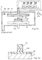
- the multiple-layer structure is placed in a vacuum chamber 15a of an anode-coupled parallel-plate reactive ion etching system 15 as shown in figure 4C.
- a reactor 15b defines the vacuum chamber 15a, and cathode plate 15c and an anode plate 15d are provided in the vacuum chamber 15a.
- the cathode plate 15c is grounded, and is opposed to the anode plate 15d.
- the anode plate 15d is connected to an rf power source 15e, and a gas conduit 15f is formed in the anode plate 15d.
- a gas supply sub-system 15g is connected to the gas conduit 15f, and etching gas is supplied from the gas supply sub-system 15g through the gas conduit 15f to the vacuum chamber 15a.
- the vacuum chamber 15a is further connected to a vacuum pump 15h, and the vacuum pump 15f develops vacuum in the vacuum chamber 15a.
- the etching gas contains sulfur hexafluoride expressed as SF 6 , hydrogen bromide expressed as HBr and oxygen.
- the hydrogen bromide of the etching gas ranges from 3 percent to 10 percent by volume. If the hydrogen bromide is less than 3 percent, the selectivity of the etching gas is insufficient. On the other hand, if the hydrogen bromide is greater than 10 percent, the dispersion of the etching speed is too large on the upper surface of the silicon nitride layer 13.
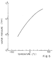
- the hydrogen bromide is larger in vapor pressure than the boron tribromide as shown in figure 5. Even through a heater is not provided for the gas supply sub-system 15g, the hydrogen bromide is not liquefied, and does not clog the gas pipe and the gas conduit 15f. Thus, the etching gas is stable and safety by virtue of the hydrogen bromide.
- the vacuum pump 15f evacuates the air in the vacuum chamber 15a, and the etching gas is supplied form the gas supply sub-system 15g to the vacuum chamber 15a.
- the flow rate of the sulfur hexafluoride, the flow rate of the hydrogen bromide and the flow rate of the oxygen are respectively regulated to 200 sccm, 15 sccm and 10 sccm, and the vacuum pump 15f maintains the vacuum chamber at 850 milli-torr.
- the rf power source 15e supplies alternating current at 13.56 MHz, and the electric power is regulated to 150 watts.
- the photo-resist etching mask 14 partially exposes the silicon nitride layer 13 to the etching gas, and the etching is isotropically carried out until the silicon oxide layer 12 is exposed.
- the etching rate to the silicon nitride is 40 nanometers per minute, and the etching gas etches the silicon oxide at 5 nanometers per minute. Therefore, the selectivity of the etching gas is 8, and is large enough to selectively etch the silicon nitride layer 13 on the silicon oxide layer 12. For this reason, even if the etching gas excessively etches the multiple-layer structure, the silicon substrate 11 is never exposed as shown in figure 4D.
- Figures 6A to 6D illustrate the process sequence applied to a multiple-layer structure having a step portion.
- the process starts with preparation of a silicon substrate 21, and a silicon oxide layer 22 is deposited on a major surface of the silicon substrate 21.
- Polysilicon is deposited on the silicon oxide layer 22, and the polysilicon layer is patterned into an accumulating electrode 23 by using lithographic techniques.
- Silicon oxide is deposited to 10 nanometers thick over the entire surface of the resultant structure by using a chemical vapor deposition, and a silicon oxide layer covers the accumulating electrode 23 and the silicon oxide layer 22 extending on both sides of the accumulating electrode 23.
- silicon nitride is deposited to 10 nanometers thick over the silicon oxide layer 24 by using a chemical vapor deposition, and the silicon oxide layer 24 is overlain by a silicon nitride layer 25.
- the side surface of the accumulating electrode 23 and the silicon oxide layer 22 form a step portion, and the step configuration is transferred through the silicon oxide layer 24 to the silicon nitride layer 25 as encircled by dot-and-dash line 26 as shown in figure 6A.
- the silicon substrate 21, the silicon oxide layer 22, the accumulating electrode 23, the silicon oxide layer 24 and the silicon nitride layer 25 as a whole constitute a multiple-layer structure.
- Photo-resist is spread over the entire surface of the silicon nitride layer 25, and the silicon nitride layer 25 is overlain by a photo-resist layer.
- a pattern image is optically transferred to the photo-resist layer, and the photo-resist layer is developed into a photo-resist etching mask 27 as shown in figure 6B.
- the isotropic dry etching is carried out under the same conditions as described hereinbefore, and the silicon nitride layer 25 uncovered with the photo-resist etching mask 27 is removed from the multiple-layer structure as shown in figure 6D.
- the isotropy results in a silicon nitride strip 25a beneath the photo-resist etching mask 27 without a residual piece at the step portion.
- the photo-resist etching mask 27 is stripped off, and a counter electrode is finally formed in such a manner as to be opposite to the accumulating electrode 23.
- the hydrogen bromide has a large vapor pressure, and causes the etching gas to selectively etch the silicon nitride layer 13 under the large selectivity to the silicon oxide. For this reason, the process of patterning a silicon nitride layer according to the present invention achieves a miniature silicon nitride pattern. Moreover, the etching gas isotropically patterns the silicon nitride layer under the above described etching conditions.
- Figures 7A to 7D illustrate another process of patterning a silicon nitride layer embodying the present invention.
- the process starts with preparation of a silicon substrate 31, and a surface portion of the silicon substrate 31 is thermally oxidized.
- a silicon oxide layer 32 is grown to 10 nanometers thick over the silicon substrate 31.
- the silicon oxide layer 32 may be deposited by using the chemical vapor deposition.
- Silicon nitride is deposited to 150 nanometers thick over the entire surface of the silicon oxide layer 32, and the silicon oxide layer 32 is overlain by a silicon nitride layer 33 as shown in figure 7A.
- the silicon substrate 31, the silicon oxide layer 32 and the silicon nitride layer 33 as a whole constitute a multiple-layer structure.
- Photo-resist is spread over the entire surface of the silicon nitride layer 33, and the silicon nitride layer 33 is overlain by a photo-resist layer.
- a pattern image is optically transferred to the photo-resist layer, and the photo-resist layer is developed into a photo-resist etching mask 34 as shown in figure 7B.
- An anisotropic etching is firstly carried out.
- the anisotropic etching conditions are regulated as follows.
- the flow rate of the sulfur hexafluoride and the flow rate of the methine trifluoride (CHF 3 ) are 50 sccm and 5 sccm, respectively, and the vacuum chamber 15a is maintained at 300 milli-torr.
- the radio frequency is regulated to 13.56 MHz, and the rf power source 15e applies 250 watts to the anode plate 15d.
- the etching gas anisotropically removes the silicon nitride layer 33 exposed thereto, and the etching rate to the silicon nitride and the etching rate to the silicon oxide are 180 nanometers per minute and 60 nanometers per minute, respectively. Therefore, the selectivity between the silicon nitride and the silicon oxide is 3.
- the etching time is controlled by using an etching end point detector (not shown).
- the anisotropic etching forms sharp edges of a silicon nitride strip 33a on the silicon oxide layer 32. However, residual silicon nitride pieces are left on the multi-layer structure due to a dispersion of the etching speed.
- the isotropic etching is carried out by using the etching gas containing the sulfur hexafluoride, the hydrogen bromide and the oxygen.
- the isotropic etching conditions are as follows.
- the flow rate of the sulfur hexafluoride, the flow rate of the hydrogen bromide and the flow rate of the oxygen are respectively regulated to 200 sccm, 15 sccm and 10 sccm, and the vacuum pump maintains the vacuum chamber 15a at 850 milli-torr.
- the rf power source 15e supplies alternating current at 13.56 MHz, and the electric power is regulated to 150 watts.
- the isotropic etching removes the residual silicon nitride pieces from the multiple-layer structure without etching the silicon oxide layer 32 as shown in figure 7D.
- the photo-resist etching mask 34 is stripped off, and the silicon nitride strip 33a is left on she silicon oxide layer 32.
- the thick silicon nitride layer 33 is patterned into the silicon nitride strip 33a without a residual silicon nitride piece by using the combination of the anisotropic etching and the isotropic etching according to the present invention.
- the etching gas containing the sulfur hexafluoride, the hydrogen bromide and the oxygen isotropically etches a silicon nitride layer with a large selectivity.
- the hydrogen bromide has a large vapor pressure, and is not liquefied without a heater. For this reason, the etching gas is safety and stable in composition.
- Any substance is available in so far as the substance is smaller in etching rate than the silicon nitride.
- the silicon nitride layer may be uniformly etched without an etching mask for making up a hole or recess. For this reason, an etching mask is not a indispensable feature of the present invention.
Landscapes
- Drying Of Semiconductors (AREA)
- ing And Chemical Polishing (AREA)
Applications Claiming Priority (2)
| Application Number | Priority Date | Filing Date | Title |
|---|---|---|---|
| JP124976/95 | 1995-05-24 | ||
| JP7124976A JPH08321484A (ja) | 1995-05-24 | 1995-05-24 | 半導体装置の製造方法 |
Publications (2)
| Publication Number | Publication Date |
|---|---|
| EP0744767A2 true EP0744767A2 (de) | 1996-11-27 |
| EP0744767A3 EP0744767A3 (de) | 1998-03-11 |
Family
ID=14898876
Family Applications (1)
| Application Number | Title | Priority Date | Filing Date |
|---|---|---|---|
| EP96108189A Withdrawn EP0744767A3 (de) | 1995-05-24 | 1996-05-22 | Verfahren zum Ätzen einer Siliziumnitrid-Schicht unter Verwendung eines Schwefelhexafluorid, Bromwasserstoff und Sauerstoff enthaltenden Ätzgases |
Country Status (4)
| Country | Link |
|---|---|
| US (1) | US5695602A (de) |
| EP (1) | EP0744767A3 (de) |
| JP (1) | JPH08321484A (de) |
| TW (1) | TW399265B (de) |
Cited By (1)
| Publication number | Priority date | Publication date | Assignee | Title |
|---|---|---|---|---|
| US6743727B2 (en) | 2001-06-05 | 2004-06-01 | International Business Machines Corporation | Method of etching high aspect ratio openings |
Families Citing this family (9)
| Publication number | Priority date | Publication date | Assignee | Title |
|---|---|---|---|---|
| US5851890A (en) * | 1997-08-28 | 1998-12-22 | Lsi Logic Corporation | Process for forming integrated circuit structure with metal silicide contacts using notched sidewall spacer on gate electrode |
| US6121154A (en) * | 1997-12-23 | 2000-09-19 | Lam Research Corporation | Techniques for etching with a photoresist mask |
| US6207544B1 (en) * | 1998-12-09 | 2001-03-27 | Advanced Micro Devices, Inc. | Method of fabricating ultra thin nitride spacers and device incorporating same |
| JP2002134472A (ja) * | 2000-10-20 | 2002-05-10 | Mitsubishi Electric Corp | エッチング方法、エッチング装置および半導体装置の製造方法 |
| KR100455723B1 (ko) | 2001-09-13 | 2004-11-12 | 주식회사 하이닉스반도체 | 비트라인 형성방법 |
| KR100561522B1 (ko) * | 2003-12-30 | 2006-03-16 | 동부아남반도체 주식회사 | 반도체 소자 분리막 형성 방법 |
| JP4488999B2 (ja) * | 2005-10-07 | 2010-06-23 | 株式会社日立ハイテクノロジーズ | エッチング方法およびエッチング装置 |
| JP4925314B2 (ja) * | 2007-05-30 | 2012-04-25 | カシオ計算機株式会社 | 窒化シリコン膜のドライエッチング方法および薄膜トランジスタの製造方法 |
| CN113097053B (zh) * | 2021-03-26 | 2024-03-26 | 北京北方华创微电子装备有限公司 | 氧化硅纤维的制备方法和氧化硅纤维 |
Family Cites Families (8)
| Publication number | Priority date | Publication date | Assignee | Title |
|---|---|---|---|---|
| JPS5825742B2 (ja) * | 1979-12-22 | 1983-05-30 | 富士通株式会社 | プラズマエッチング処理方法及び処理装置 |
| JPS57210631A (en) * | 1981-06-19 | 1982-12-24 | Toshiba Corp | Reactive type ion etching method |
| JP2685196B2 (ja) * | 1988-01-18 | 1997-12-03 | 松下電器産業株式会社 | ドライエッチング方法 |
| JPH02128422A (ja) * | 1988-11-07 | 1990-05-16 | Fujitsu Ltd | 半導体装置の製造方法 |
| JPH02166733A (ja) * | 1988-12-21 | 1990-06-27 | Fujitsu Ltd | 半導体装置の製造方法 |
| EP0424299A3 (en) * | 1989-10-20 | 1991-08-28 | International Business Machines Corporation | Selective silicon nitride plasma etching |
| JPH03237716A (ja) * | 1990-02-14 | 1991-10-23 | Fujitsu Ltd | 半導体装置の製造方法 |
| JPH04275423A (ja) * | 1991-03-04 | 1992-10-01 | Fujitsu Ltd | 半導体装置の製造方法 |
-
1995
- 1995-05-24 JP JP7124976A patent/JPH08321484A/ja active Pending
-
1996
- 1996-05-21 TW TW085105972A patent/TW399265B/zh active
- 1996-05-21 US US08/650,983 patent/US5695602A/en not_active Expired - Fee Related
- 1996-05-22 EP EP96108189A patent/EP0744767A3/de not_active Withdrawn
Cited By (1)
| Publication number | Priority date | Publication date | Assignee | Title |
|---|---|---|---|---|
| US6743727B2 (en) | 2001-06-05 | 2004-06-01 | International Business Machines Corporation | Method of etching high aspect ratio openings |
Also Published As
| Publication number | Publication date |
|---|---|
| TW399265B (en) | 2000-07-21 |
| JPH08321484A (ja) | 1996-12-03 |
| US5695602A (en) | 1997-12-09 |
| EP0744767A3 (de) | 1998-03-11 |
Similar Documents
| Publication | Publication Date | Title |
|---|---|---|
| US7288482B2 (en) | Silicon nitride etching methods | |
| US5447598A (en) | Process for forming resist mask pattern | |
| US5007982A (en) | Reactive ion etching of silicon with hydrogen bromide | |
| JPH08250466A (ja) | シリコン基板に深くて垂直な構造を作製する方法 | |
| US5695602A (en) | Process of etching silicon nitride layer by using etching gas containing sulfur hexafluoride, hydrogen bromide and oxygen | |
| US5914280A (en) | Deep trench etch on bonded silicon wafer | |
| WO1992017900A1 (en) | HIGH DURABILITY MASK FOR DRY ETCHING OF GaAs | |
| US5686345A (en) | Trench mask for forming deep trenches in a semiconductor substrate, and method of using same | |
| US20070090446A1 (en) | Hardmask etch for gate polyetch | |
| JP2001520458A (ja) | フッ素置換炭化水素とアセチレンからなり窒化物に対して高選択性を有する混合物を用いた酸化物エッチング方法 | |
| US5853602A (en) | Method of dry etching for patterning refractory metal layer improved in etching rate, anisotropy and selectivity to silicon oxide | |
| US5496200A (en) | Sealed vacuum electronic devices | |
| JPH05304119A (ja) | ポリシリコン膜のエッチング方法 | |
| US5767017A (en) | Selective removal of vertical portions of a film | |
| US4764249A (en) | Method for producing a coating layer for semiconductor technology and also use of the coating layer | |
| JPH10261713A (ja) | 半導体装置の製造方法 | |
| JPH05259269A (ja) | 素子分離領域の形成方法 | |
| US4407850A (en) | Profile control photoresist | |
| US5180466A (en) | Process for dry etching a silicon nitride layer | |
| KR100374955B1 (ko) | 반도체 장치의 제조 방법 | |
| JPH08288256A (ja) | トレンチエッチング方法 | |
| JP2008135534A (ja) | 有底の溝を有する半導体基板の製造方法 | |
| JP3773785B2 (ja) | 半導体装置の製造方法 | |
| JPH0346252A (ja) | 半導体集積回路の製造方法 | |
| EP0517627A1 (de) | Aufgebrachte Kohlenstoffmaske zum Trockenätzen von Silizium |
Legal Events
| Date | Code | Title | Description |
|---|---|---|---|
| PUAI | Public reference made under article 153(3) epc to a published international application that has entered the european phase |
Free format text: ORIGINAL CODE: 0009012 |
|
| AK | Designated contracting states |
Kind code of ref document: A2 Designated state(s): DE FR GB |
|
| PUAL | Search report despatched |
Free format text: ORIGINAL CODE: 0009013 |
|
| AK | Designated contracting states |
Kind code of ref document: A3 Designated state(s): DE FR GB |
|
| 17P | Request for examination filed |
Effective date: 19980629 |
|
| STAA | Information on the status of an ep patent application or granted ep patent |
Free format text: STATUS: THE APPLICATION HAS BEEN WITHDRAWN |
|
| 18W | Application withdrawn |
Withdrawal date: 19990629 |