EP0707965A2 - Substrat für einen Flüssigkeitsstrahlkopf, Flüssigkeitsstrahlkopf zur Verwendung desselben und diesen verwendender Flüssigkeitsstrahlapparat - Google Patents
Substrat für einen Flüssigkeitsstrahlkopf, Flüssigkeitsstrahlkopf zur Verwendung desselben und diesen verwendender Flüssigkeitsstrahlapparat Download PDFInfo
- Publication number
- EP0707965A2 EP0707965A2 EP95116690A EP95116690A EP0707965A2 EP 0707965 A2 EP0707965 A2 EP 0707965A2 EP 95116690 A EP95116690 A EP 95116690A EP 95116690 A EP95116690 A EP 95116690A EP 0707965 A2 EP0707965 A2 EP 0707965A2
- Authority
- EP
- European Patent Office
- Prior art keywords
- energy generating
- ejection energy
- ejection
- liquid
- interval
- Prior art date
- Legal status (The legal status is an assumption and is not a legal conclusion. Google has not performed a legal analysis and makes no representation as to the accuracy of the status listed.)
- Granted
Links
- 239000000758 substrate Substances 0.000 title claims abstract description 34
- 239000007788 liquid Substances 0.000 title claims abstract description 33
- 239000000463 material Substances 0.000 claims description 3
- 230000008878 coupling Effects 0.000 claims 1
- 238000010168 coupling process Methods 0.000 claims 1
- 238000005859 coupling reaction Methods 0.000 claims 1
- 238000007599 discharging Methods 0.000 claims 1
- 239000011295 pitch Substances 0.000 description 21
- 239000010410 layer Substances 0.000 description 6
- 238000005520 cutting process Methods 0.000 description 5
- 238000004519 manufacturing process Methods 0.000 description 5
- VYPSYNLAJGMNEJ-UHFFFAOYSA-N Silicium dioxide Chemical compound O=[Si]=O VYPSYNLAJGMNEJ-UHFFFAOYSA-N 0.000 description 4
- 230000008901 benefit Effects 0.000 description 3
- 230000000694 effects Effects 0.000 description 3
- 238000000034 method Methods 0.000 description 3
- 238000000206 photolithography Methods 0.000 description 3
- 238000004544 sputter deposition Methods 0.000 description 3
- 229910052782 aluminium Inorganic materials 0.000 description 2
- 229910052681 coesite Inorganic materials 0.000 description 2
- 238000005336 cracking Methods 0.000 description 2
- 229910052906 cristobalite Inorganic materials 0.000 description 2
- 239000000377 silicon dioxide Substances 0.000 description 2
- 235000012239 silicon dioxide Nutrition 0.000 description 2
- 229910052682 stishovite Inorganic materials 0.000 description 2
- 229910052905 tridymite Inorganic materials 0.000 description 2
- 229910003862 HfB2 Inorganic materials 0.000 description 1
- 229910052581 Si3N4 Inorganic materials 0.000 description 1
- XAGFODPZIPBFFR-UHFFFAOYSA-N aluminium Chemical compound [Al] XAGFODPZIPBFFR-UHFFFAOYSA-N 0.000 description 1
- 239000007772 electrode material Substances 0.000 description 1
- 239000004744 fabric Substances 0.000 description 1
- 239000011521 glass Substances 0.000 description 1
- 238000005338 heat storage Methods 0.000 description 1
- 239000000203 mixture Substances 0.000 description 1
- 230000004048 modification Effects 0.000 description 1
- 238000012986 modification Methods 0.000 description 1
- 239000011368 organic material Substances 0.000 description 1
- 230000003647 oxidation Effects 0.000 description 1
- 238000007254 oxidation reaction Methods 0.000 description 1
- 230000002265 prevention Effects 0.000 description 1
- 230000008569 process Effects 0.000 description 1
- 230000001681 protective effect Effects 0.000 description 1
- 239000011241 protective layer Substances 0.000 description 1
- 239000011347 resin Substances 0.000 description 1
- 229920005989 resin Polymers 0.000 description 1
- 230000004044 response Effects 0.000 description 1
Images


Classifications
-
- B—PERFORMING OPERATIONS; TRANSPORTING
- B41—PRINTING; LINING MACHINES; TYPEWRITERS; STAMPS
- B41J—TYPEWRITERS; SELECTIVE PRINTING MECHANISMS, i.e. MECHANISMS PRINTING OTHERWISE THAN FROM A FORME; CORRECTION OF TYPOGRAPHICAL ERRORS
- B41J2/00—Typewriters or selective printing mechanisms characterised by the printing or marking process for which they are designed
- B41J2/005—Typewriters or selective printing mechanisms characterised by the printing or marking process for which they are designed characterised by bringing liquid or particles selectively into contact with a printing material
- B41J2/01—Ink jet
- B41J2/135—Nozzles
- B41J2/14—Structure thereof only for on-demand ink jet heads
- B41J2/14016—Structure of bubble jet print heads
- B41J2/14088—Structure of heating means
- B41J2/14112—Resistive element
- B41J2/14129—Layer structure
-
- B—PERFORMING OPERATIONS; TRANSPORTING
- B41—PRINTING; LINING MACHINES; TYPEWRITERS; STAMPS
- B41J—TYPEWRITERS; SELECTIVE PRINTING MECHANISMS, i.e. MECHANISMS PRINTING OTHERWISE THAN FROM A FORME; CORRECTION OF TYPOGRAPHICAL ERRORS
- B41J2/00—Typewriters or selective printing mechanisms characterised by the printing or marking process for which they are designed
- B41J2/005—Typewriters or selective printing mechanisms characterised by the printing or marking process for which they are designed characterised by bringing liquid or particles selectively into contact with a printing material
- B41J2/01—Ink jet
- B41J2/135—Nozzles
- B41J2/145—Arrangement thereof
- B41J2/155—Arrangement thereof for line printing
-
- B—PERFORMING OPERATIONS; TRANSPORTING
- B41—PRINTING; LINING MACHINES; TYPEWRITERS; STAMPS
- B41J—TYPEWRITERS; SELECTIVE PRINTING MECHANISMS, i.e. MECHANISMS PRINTING OTHERWISE THAN FROM A FORME; CORRECTION OF TYPOGRAPHICAL ERRORS
- B41J2/00—Typewriters or selective printing mechanisms characterised by the printing or marking process for which they are designed
- B41J2/005—Typewriters or selective printing mechanisms characterised by the printing or marking process for which they are designed characterised by bringing liquid or particles selectively into contact with a printing material
- B41J2/01—Ink jet
- B41J2/135—Nozzles
- B41J2/16—Production of nozzles
- B41J2/1601—Production of bubble jet print heads
-
- B—PERFORMING OPERATIONS; TRANSPORTING
- B41—PRINTING; LINING MACHINES; TYPEWRITERS; STAMPS
- B41J—TYPEWRITERS; SELECTIVE PRINTING MECHANISMS, i.e. MECHANISMS PRINTING OTHERWISE THAN FROM A FORME; CORRECTION OF TYPOGRAPHICAL ERRORS
- B41J2/00—Typewriters or selective printing mechanisms characterised by the printing or marking process for which they are designed
- B41J2/005—Typewriters or selective printing mechanisms characterised by the printing or marking process for which they are designed characterised by bringing liquid or particles selectively into contact with a printing material
- B41J2/01—Ink jet
- B41J2/135—Nozzles
- B41J2/16—Production of nozzles
- B41J2/1621—Manufacturing processes
- B41J2/1623—Manufacturing processes bonding and adhesion
-
- B—PERFORMING OPERATIONS; TRANSPORTING
- B41—PRINTING; LINING MACHINES; TYPEWRITERS; STAMPS
- B41J—TYPEWRITERS; SELECTIVE PRINTING MECHANISMS, i.e. MECHANISMS PRINTING OTHERWISE THAN FROM A FORME; CORRECTION OF TYPOGRAPHICAL ERRORS
- B41J2/00—Typewriters or selective printing mechanisms characterised by the printing or marking process for which they are designed
- B41J2/005—Typewriters or selective printing mechanisms characterised by the printing or marking process for which they are designed characterised by bringing liquid or particles selectively into contact with a printing material
- B41J2/01—Ink jet
- B41J2/135—Nozzles
- B41J2/16—Production of nozzles
- B41J2/1621—Manufacturing processes
- B41J2/1631—Manufacturing processes photolithography
-
- B—PERFORMING OPERATIONS; TRANSPORTING
- B41—PRINTING; LINING MACHINES; TYPEWRITERS; STAMPS
- B41J—TYPEWRITERS; SELECTIVE PRINTING MECHANISMS, i.e. MECHANISMS PRINTING OTHERWISE THAN FROM A FORME; CORRECTION OF TYPOGRAPHICAL ERRORS
- B41J2/00—Typewriters or selective printing mechanisms characterised by the printing or marking process for which they are designed
- B41J2/005—Typewriters or selective printing mechanisms characterised by the printing or marking process for which they are designed characterised by bringing liquid or particles selectively into contact with a printing material
- B41J2/01—Ink jet
- B41J2/135—Nozzles
- B41J2/16—Production of nozzles
- B41J2/1621—Manufacturing processes
- B41J2/1635—Manufacturing processes dividing the wafer into individual chips
-
- B—PERFORMING OPERATIONS; TRANSPORTING
- B41—PRINTING; LINING MACHINES; TYPEWRITERS; STAMPS
- B41J—TYPEWRITERS; SELECTIVE PRINTING MECHANISMS, i.e. MECHANISMS PRINTING OTHERWISE THAN FROM A FORME; CORRECTION OF TYPOGRAPHICAL ERRORS
- B41J2/00—Typewriters or selective printing mechanisms characterised by the printing or marking process for which they are designed
- B41J2/005—Typewriters or selective printing mechanisms characterised by the printing or marking process for which they are designed characterised by bringing liquid or particles selectively into contact with a printing material
- B41J2/01—Ink jet
- B41J2/135—Nozzles
- B41J2/16—Production of nozzles
- B41J2/1621—Manufacturing processes
- B41J2/164—Manufacturing processes thin film formation
- B41J2/1642—Manufacturing processes thin film formation thin film formation by CVD [chemical vapor deposition]
-
- B—PERFORMING OPERATIONS; TRANSPORTING
- B41—PRINTING; LINING MACHINES; TYPEWRITERS; STAMPS
- B41J—TYPEWRITERS; SELECTIVE PRINTING MECHANISMS, i.e. MECHANISMS PRINTING OTHERWISE THAN FROM A FORME; CORRECTION OF TYPOGRAPHICAL ERRORS
- B41J2/00—Typewriters or selective printing mechanisms characterised by the printing or marking process for which they are designed
- B41J2/005—Typewriters or selective printing mechanisms characterised by the printing or marking process for which they are designed characterised by bringing liquid or particles selectively into contact with a printing material
- B41J2/01—Ink jet
- B41J2/135—Nozzles
- B41J2/16—Production of nozzles
- B41J2/1621—Manufacturing processes
- B41J2/164—Manufacturing processes thin film formation
- B41J2/1646—Manufacturing processes thin film formation thin film formation by sputtering
-
- B—PERFORMING OPERATIONS; TRANSPORTING
- B41—PRINTING; LINING MACHINES; TYPEWRITERS; STAMPS
- B41J—TYPEWRITERS; SELECTIVE PRINTING MECHANISMS, i.e. MECHANISMS PRINTING OTHERWISE THAN FROM A FORME; CORRECTION OF TYPOGRAPHICAL ERRORS
- B41J2202/00—Embodiments of or processes related to ink-jet or thermal heads
- B41J2202/01—Embodiments of or processes related to ink-jet heads
- B41J2202/20—Modules
Definitions
- the present invention relates to an element chip, which comprises an energy generating element for generating ejection energy to be used for ejecting recording liquid (ink or the like) in the form of a flying liquid droplet from an ejection outlet (orifice), and is employed in an ink jet head installed in an ink jet recording apparatus, which generates records by adhering the ejected liquid droplets to the recording medium.
- the present invention relates to such an element chip in which plural energy generating elements for generating the ink ejection energy to be used for ejecting the ink are arranged in a predetermined manner.
- the present invention also relates to an ink jet head, in which plural ejection energy generating elements are arranged in a predetermined manner, and an ink jet apparatus comprising such a head.
- the ink jet recording method is a recording method in which ink (recording liquid) is ejected from an orifice, or orifices, of a recording head, so that the ejected ink is adhered to recording medium, such as paper, to create record. It has various advantages. For example, it generates only an extremely small amount of noise, and can record at a high speed. In addition, it can record on plain paper; it does not require dedicated paper with special composition. Therefore, various types of ink jet recording head have been developed.
- This type of ink jet head is produced in the following manner.
- the electrothermal transducers and electrodes are formed on a substrate, and are covered with a protective film as needed. Then, a top plate, in which liquid paths and a liquid chamber are formed, is joined with the substrate.
- the ejection energy for ejecting the ink from this type of recording head is generated by the electrothermal transducer comprising a pair of electrodes, and a heat generating resistor element disposed between the pair of electrodes. More specifically, an electric signal is applied to the electrode to cause the heat generating resistor element to generate heat. As heat is generated by the heat generating resistor, the ink adjacent to the heat generating resistor disposed within the ink path is instantaneously heated, generating bubbles. As the volume of the bubble quickly grows and contracts, the ink is ejected in the form of a liquid droplet.
- plural element chips in which a predetermined number of heat generating resistor elements are arranged at a predetermined pitch, are employed. More specifically, the plural element chips are precisely aligned on a supporting member, which has a width correspondent to the recording width, so that the recording width for A3 paper can be entirely covered with the aligned heat generating resistor elements, at the same pitch as the heat generating resistor element pitch in each of the element chips.
- the portions of the element chip, or, in the worst case, the heat generating resistor element itself, is liable to be damaged by chipping and/or shell cracking that could occur during the cutting process.
- the heat generating resistor elements located near the end, relative to the alignment direction, of each element chip are aligned at a smaller pitch than the normal (main) pitch for the heat generating resistor elements located across the middle of the same element chip; they are inwardly displaced, relative to the end of each element chip.
- the margin which is reserved for cutting the substrate to separate each element chip, can be increased to prevent the heat generating resistor element from being damaged by chipping, shell cracking, and the like.
- a stepped portion may be formed between the heat generating resistor element adjacent to the cutting margin, and the cutting margin, so that the effects of the aforementioned structure can be enhanced.
- Figure 1 is a schematic view of an embodiment of the present invention.
- Figure 2 is a schematic view of another embodiment of the present invention.
- Figure 3 is a schematic view of a further embodiment of the present invention:
- Figure 4 is a schematic sectional view of the embodiment of the present invention, illustrating a state of chipping which occurs when a substrate structured according to the present invention is cut.
- Figure 5 is a schematic view of a conventional element chip, illustrating a state of chipping which occurs when a conventionally structured element chip is cut.
- Figure 6 is a schematic view of another state of chipping which occurs when the conventionally structured element chip is cut.
- Figure 7 is an exploded perspective view of an widened head, in which plural element chips in accordance with the present invention are aligned in a predetermined manner.
- Figure 8 is a conceptual view of an ink jet recording apparatus employing a full-line head in accordance with the present invention.
- Figure 9 is a perspective view of an ink jet recording apparatus employing the ink jet head in accordance with the present invention.
- on the substrate means “on the substrate,” as well as “immediately below the plane of the substrate surface.”
- the liquid to be ejected is not limited to ink; any liquid is usable as long as it can be ejected by the ejection head in accordance with the present invention.
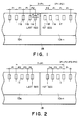
- FIG. 1 is a schematic view of an embodiment of the present invention.
- a reference numeral 11 designates a heat generating resistor element (ejection heater) as an ejection energy generating member.
- Each ejection heater comprises a heat generating resistor layer 12, and a pair of electrodes (unillustrated), and generates heat as a voltage is applied to the heat generating resistor layer 12 through the pair of electrodes.
- One of the electrodes is connected to an independent electrode (unillustrated), and the other is connected to a common electrode (unillustrated).
- the heat generating resistor elements 11 are aligned on the element substrate at a predetermined pitch P1, except that the first and last heat generating resistor elements of each element chip, that is, the heat generating resistor element located at each end, in the alignment direction, of each element chip, is aligned at a shorter pitch P2 than those segments located between the first and last elements. Further, counting from left to right in Figure 1, the distance between the last element 11c of the first element chip, and the first element 11d of the next element chip is rendered greater than P1. Lastly, the distance between the second element 11b, counting from right to left, of the first element chip, and the second segment 11e, counting from left to right, of the next element chip, is set at a distance of approximately 3 x P1. Therefore, plural element chips can be aligned in a straight line, so that the alignment pitch for the heat generating resistor elements can be rendered substantially uniform across the entire length of the alignment.
- FIG 2 is a schematic view of another embodiment of the present invention, in which three different pitches (P2, P3 and P4), which are shorter than the normal alignment pitch P1, are employed.
- the relationship among the different pitches is: P1 > P2 > P3 > P4.
- the relationship among the different pitches is not limited to the above. In other words, such factors as the number of alignment pitches different from the regular pitch P1, the positional relationship among the different pitches, and the like, may be optionally combined to obtain the same effect as the present invention.
- the distance between the second ejection heater, counting from left to right, of one element chip, and the second ejection heater, counting from right to left, of the next element chip is set at approximately three times the pitch for the ejection heaters located at the center portion of the element chip.
- the distance between the third ejection heater, counting from left to right, of one element chip, and the third ejection heater, counting from right to left, of the next element chip is set at approximately seven times the pitch for the ejection heaters located at the center portion of the element chip.
- the element chip can be cut at a point close to the ejection heater, without damaging it; therefore, even when plural element chips are continuously aligned in a straight line, the ejection heater intervals can be rendered generally uniform.
- the ejection heater intervals are not limited to those described above. Needless to say, the distance between the second ejection heaters of two adjacent element chips, counting away from the joint, may be set at approximately five times the interval between the adjacent ejection heaters located at the central portion of each element chip.
- the interval between the adjacent two ejection heaters located near each end of each element chip is adjusted.
- the ejection heater interval may be adjusted only at the element chip end on the joint side.
- FIG 3 is a schematic section (at A - A line in Figure 1) of the embodiment of the present invention, illustrating a stepped portion 19 for preventing the advance of the crack, such as pitching or shell crack, which occurs while the substrate is cut.
- the stepped portion 19 can be formed using, for example, the same manufacturing step and the same material (Al, Cu or the like) for wiring electrode, without increasing the number of manufacturing steps. If cost is not a concern, the stepped portion 19 may be formed of a separate material (organic material such as polyimede).
- Figure 4 is a schematic sectional view of the embodiment of the present invention, illustrating how the advance of the crack is prevented while the substrate is cut. Even if a crack 17 occurs as the chip substrate 10 is cut across a margin 16, the advance of the crack can be stopped at the stepped portion 19.
- Figures 5 and 6 are schematic sections of the conventional chip structure, illustrating how the crack advances while the substrate is cut.
- the recording head described above can be produced following the steps described below.
- a 1 - 3 ⁇ m thick SiO2 film as a heat storage layer 13 is formed on a Si wafer, using thermal oxidation.
- a 400 - 2,000 ⁇ thick HfB2 film which becomes the heat generating resistor layer, a 10 - 100 ⁇ thick Ti film which becomes an adhesion enhancement layer, and a 3,000 - 10,000 ⁇ thick Al (wiring electrode material), are deposited in this order by sputtering.
- the heat generating resistors, electrodes, and the like, of desired patterns are formed by photolithography.
- a 1 - 2 ⁇ m thick film of SiO2 or Si3N4 as a protective layer 14 is formed by CVD or sputtering.
- a 2,000 - 5,000 ⁇ thick Ta film as a cavitation resistance layer 15 is deposited by sputtering.
- the desired patterns are formed by photolithography to complete the element chip 10.
- the element chips 10 are precisely aligned on a supporting member 18 (for example, Al substrate) with excellent heat radiating properties, and fixed thereto by die bonding.
- a supporting member 18 for example, Al substrate
- a glass plate (unillustrated), which has grooves for forming at least the ink paths and orifices, is aligned on the the chip substrate, so that the groove portions for forming the ink paths are properly located in relation to the heat generating portion formed on the chip substrate, and is glued thereto.
- the walls for forming at least the ink paths and ejection orifices may be formed on the chip substrate by photolithography which uses photosensitive resin or the like, and then, the walls may be covered to complete the recording head.
- FIG. 7 illustrates such an example, in which plural element chips 100, in which plural heat generating resistors 101 are aligned in a straight line, are aligned in a straight line on a supporting member (base plate) of aluminum (Al) or the like. Each element chip is connected to the contact pad of the wiring chip through a connector 102.
- the top plate 200 which is grooved to form an ink path for each heat generating resistor, is attached to the plural element chips aligned as described above, to complete a wider head.
- Figure 8 is a schematic perspective view of a so-called full-line type recording head, the width of which corresponds to the recording width of the recording medium, and a recording apparatus, in which the full-line type recording head is mounted.
- the present invention displays the most outstanding effects when applied to the full-line recording head illustrated in Figure 8.
- a reference numeral 6 designates a fill-line recording head.
- the ink is ejected from this recording head, in response to signals supplied from driving signal supplying means (unillustrated), toward a recording medium 80 such as paper or fabric conveyed by a conveyer roller 90, whereby recording is made on the recording medium 80.
- driving signal supplying means unillustrated
- a recording medium 80 such as paper or fabric conveyed by a conveyer roller 90
- Figure 9 shows such a recording apparatus that employs a small recording head comprising only one or two element chips.
- the recording apparatus illustrated in Figure 9 comprises a recording head cartridge constituted of an independently exchangeable ink container 70 and an independently exchangeable recording head portion 60. It also is comprises: a motor 81 as a driving power source, which drives the carriage; a conveyer roller 90 for conveying a recording medium 80; and a carriage shaft 85 for transmitting the driving force from the driving power source to the carriage. Further, it comprises signal supplying means for supplying an ink ejection signal to the recording head.
- the heat generating resistor pitch can be rendered substantially uniform across the entire length of the alignment, satisfying the condition for the heat generating resistor alignment.
- the ejection heater pitch can be rendered substantially uniform across the combined length of the plural chips.
- the present invention also enjoys an advantage in that the element chip in accordance with the present invention can be manufactured using the conventional process, without a need for increasing the number of manufacturing steps; therefore there is no cost increase.
- the chip substrate when cut to yield element chips, it can be cut at a point close to the heat generating resistor; therefore, plural element chips can be aligned to produce a wider recording head.
- the wider recording head can be inexpensively produced with extremely high yield.
- an ink jet apparatus capable of recording high quality images at a high speed can be inexpensively produced.
- a liquid jet element substrate having a plurality of ejection energy generating elements for generating ejection energy for ejecting liquid, arranged in an array in a direction at predetermined intervals, wherein an interval between the ejection energy generating element at an end, in the direction of the array, and the ejection energy generating element adjacent thereto is smaller than an interval between adjacent central ejection energy generating elements.
Applications Claiming Priority (3)
| Application Number | Priority Date | Filing Date | Title |
|---|---|---|---|
| JP256716/94 | 1994-10-21 | ||
| JP25671694A JP3397473B2 (ja) | 1994-10-21 | 1994-10-21 | 液体噴射ヘッド用素子基板を用いた液体噴射ヘッド、該ヘッドを用いた液体噴射装置 |
| JP25671694 | 1994-10-21 |
Publications (3)
| Publication Number | Publication Date |
|---|---|
| EP0707965A2 true EP0707965A2 (de) | 1996-04-24 |
| EP0707965A3 EP0707965A3 (de) | 1997-03-19 |
| EP0707965B1 EP0707965B1 (de) | 1999-08-11 |
Family
ID=17296472
Family Applications (1)
| Application Number | Title | Priority Date | Filing Date |
|---|---|---|---|
| EP95116690A Expired - Lifetime EP0707965B1 (de) | 1994-10-21 | 1995-10-23 | Substrat für einen Flüssigkeitsstrahlkopf, Flüssigkeitsstrahlkopf zur Verwendung desselben und diesen verwendender Flüssigkeitsstrahlapparat |
Country Status (4)
| Country | Link |
|---|---|
| US (1) | US5896147A (de) |
| EP (1) | EP0707965B1 (de) |
| JP (1) | JP3397473B2 (de) |
| DE (1) | DE69511348T2 (de) |
Cited By (6)
| Publication number | Priority date | Publication date | Assignee | Title |
|---|---|---|---|---|
| EP0811498A2 (de) * | 1996-06-07 | 1997-12-10 | Canon Kabushiki Kaisha | Flüssigkeitsausstosskopf, Vorrichtung zum Austossen von Flüssigkeit und Drucksystem |
| EP0921003A1 (de) * | 1997-12-03 | 1999-06-09 | Océ-Technologies B.V. | Tintenstrahlkopf |
| EP1238805A1 (de) * | 2001-03-06 | 2002-09-11 | Sony Corporation | Druckkopf, Drucker und Druckkopfsteuerungsverfahren |
| WO2003061975A1 (en) * | 2002-01-16 | 2003-07-31 | Xaar Technology Limited | Droplet deposition apparatus |
| EP1287995A3 (de) * | 2001-08-31 | 2003-09-10 | Canon Kabushiki Kaisha | Flüssigkeitausstosskopf and damit versehene Bilderzeugungsvorrichtung |
| CN104108241A (zh) * | 2013-04-17 | 2014-10-22 | 佳能株式会社 | 液体喷出头 |
Families Citing this family (11)
| Publication number | Priority date | Publication date | Assignee | Title |
|---|---|---|---|---|
| US6357862B1 (en) | 1998-10-08 | 2002-03-19 | Canon Kabushiki Kaisha | Substrate for ink jet recording head, ink jet recording head and method of manufacture therefor |
| US6450614B1 (en) * | 1998-12-17 | 2002-09-17 | Hewlett-Packard Company | Printhead die alignment for wide-array inkjet printhead assembly |
| US6474776B1 (en) * | 1999-03-04 | 2002-11-05 | Encad, Inc. | Ink jet cartridge with two jet plates |
| JP3576888B2 (ja) | 1999-10-04 | 2004-10-13 | キヤノン株式会社 | インクジェットヘッド用基体、インクジェットヘッド及びインクジェット装置 |
| US6435660B1 (en) | 1999-10-05 | 2002-08-20 | Canon Kabushiki Kaisha | Ink jet recording head substrate, ink jet recording head, ink jet recording unit, and ink jet recording apparatus |
| JP3720689B2 (ja) | 2000-07-31 | 2005-11-30 | キヤノン株式会社 | インクジェットヘッド用基体、インクジェットヘッド、インクジェットヘッドの製造方法、インクジェットヘッドの使用方法およびインクジェット記録装置 |
| US6672697B2 (en) | 2001-05-30 | 2004-01-06 | Eastman Kodak Company | Compensation method for overlapping print heads of an ink jet printer |
| JP2004050637A (ja) * | 2002-07-19 | 2004-02-19 | Canon Inc | インクジェットヘッド用基板、インクジェットヘッド及び該インクジェットヘッドを備えたインクジェット記録装置 |
| US7152957B2 (en) * | 2002-12-18 | 2006-12-26 | Canon Kabushiki Kaisha | Recording device board having a plurality of bumps for connecting an electrode pad and an electrode lead, liquid ejection head, and manufacturing method for the same |
| ATE548193T1 (de) * | 2006-04-07 | 2012-03-15 | Oce Tech Bv | Tintenstrahldruckkopf |
| JP4944687B2 (ja) | 2007-06-28 | 2012-06-06 | 株式会社リコー | 圧電アクチュエータ及びその製造方法、液体吐出ヘッド、画像形成装置 |
Family Cites Families (16)
| Publication number | Priority date | Publication date | Assignee | Title |
|---|---|---|---|---|
| JPH0643128B2 (ja) * | 1983-02-05 | 1994-06-08 | キヤノン株式会社 | インクジェットヘッド |
| JPS59194860A (ja) * | 1983-04-19 | 1984-11-05 | Canon Inc | 液体噴射記録ヘツド |
| JPH062414B2 (ja) * | 1983-04-19 | 1994-01-12 | キヤノン株式会社 | インクジェットヘッド |
| JPH0624855B2 (ja) * | 1983-04-20 | 1994-04-06 | キヤノン株式会社 | 液体噴射記録ヘッド |
| JPS59194867A (ja) * | 1983-04-20 | 1984-11-05 | Canon Inc | ヘッドの製造方法 |
| JPS60116452A (ja) * | 1983-11-30 | 1985-06-22 | Canon Inc | インクジェットヘッド |
| JPS60159062A (ja) * | 1984-01-31 | 1985-08-20 | Canon Inc | 液体噴射記録ヘツド |
| US4719478A (en) * | 1985-09-27 | 1988-01-12 | Canon Kabushiki Kaisha | Heat generating resistor, recording head using such resistor and drive method therefor |
| JP2846636B2 (ja) * | 1987-12-02 | 1999-01-13 | キヤノン株式会社 | インクジェット記録ヘッド用基板の作製方法 |
| US4851371A (en) * | 1988-12-05 | 1989-07-25 | Xerox Corporation | Fabricating process for large array semiconductive devices |
| US5237343A (en) * | 1989-03-24 | 1993-08-17 | Canon Kabushiki Kaisha | Ink jet head substrate, ink jet head having same and manufacturing method for ink jet head |
| JP2752486B2 (ja) * | 1989-12-29 | 1998-05-18 | キヤノン株式会社 | インクジェット記録ヘッドおよびその検査方法ならびにインクジェット記録装置 |
| EP0579338B1 (de) * | 1990-01-25 | 1997-09-17 | Canon Kabushiki Kaisha | Tintenstrahlaufzeichnungskopf, Substrat dafür und Tintenstrahlaufzeichnungsgerät |
| US5160403A (en) * | 1991-08-09 | 1992-11-03 | Xerox Corporation | Precision diced aligning surfaces for devices such as ink jet printheads |
| US5218754A (en) * | 1991-11-08 | 1993-06-15 | Xerox Corporation | Method of manufacturing page wide thermal ink-jet heads |
| US5410340A (en) * | 1993-11-22 | 1995-04-25 | Xerox Corporation | Off center heaters for thermal ink jet printheads |
-
1994
- 1994-10-21 JP JP25671694A patent/JP3397473B2/ja not_active Expired - Fee Related
-
1995
- 1995-10-23 EP EP95116690A patent/EP0707965B1/de not_active Expired - Lifetime
- 1995-10-23 DE DE69511348T patent/DE69511348T2/de not_active Expired - Fee Related
- 1995-10-23 US US08/546,962 patent/US5896147A/en not_active Expired - Fee Related
Non-Patent Citations (1)
| Title |
|---|
| None |
Cited By (14)
| Publication number | Priority date | Publication date | Assignee | Title |
|---|---|---|---|---|
| EP0811498A2 (de) * | 1996-06-07 | 1997-12-10 | Canon Kabushiki Kaisha | Flüssigkeitsausstosskopf, Vorrichtung zum Austossen von Flüssigkeit und Drucksystem |
| EP0811498A3 (de) * | 1996-06-07 | 1998-08-19 | Canon Kabushiki Kaisha | Flüssigkeitsausstosskopf, Vorrichtung zum Austossen von Flüssigkeit und Drucksystem |
| EP0921003A1 (de) * | 1997-12-03 | 1999-06-09 | Océ-Technologies B.V. | Tintenstrahlkopf |
| US6764164B2 (en) | 2001-03-06 | 2004-07-20 | Sony Corporation | Printer head, printer, and printer-head driving method |
| EP1238805A1 (de) * | 2001-03-06 | 2002-09-11 | Sony Corporation | Druckkopf, Drucker und Druckkopfsteuerungsverfahren |
| US6886899B2 (en) | 2001-03-06 | 2005-05-03 | Sony Corporation | Printer head, printer, and printer-head driving method |
| EP1287995A3 (de) * | 2001-08-31 | 2003-09-10 | Canon Kabushiki Kaisha | Flüssigkeitausstosskopf and damit versehene Bilderzeugungsvorrichtung |
| US7452056B2 (en) | 2001-08-31 | 2008-11-18 | Canon Kabushiki Kaisha | Liquid ejection head and image-forming apparatus using the same |
| US8016383B2 (en) | 2001-08-31 | 2011-09-13 | Canon Kabushiki Kaisha | Liquid ejection head and image-forming apparatus using the same |
| US8517509B2 (en) | 2001-08-31 | 2013-08-27 | Canon Kabushiki Kaisha | Liquid ejection head and image-forming apparatus using the same |
| WO2003061975A1 (en) * | 2002-01-16 | 2003-07-31 | Xaar Technology Limited | Droplet deposition apparatus |
| CN100358724C (zh) * | 2002-01-16 | 2008-01-02 | Xaar技术有限公司 | 微滴沉积装置 |
| CN104108241A (zh) * | 2013-04-17 | 2014-10-22 | 佳能株式会社 | 液体喷出头 |
| US9162459B2 (en) | 2013-04-17 | 2015-10-20 | Canon Kabushiki Kaisha | Liquid ejection head |
Also Published As
| Publication number | Publication date |
|---|---|
| JP3397473B2 (ja) | 2003-04-14 |
| DE69511348T2 (de) | 2000-04-13 |
| JPH08118642A (ja) | 1996-05-14 |
| DE69511348D1 (de) | 1999-09-16 |
| EP0707965B1 (de) | 1999-08-11 |
| US5896147A (en) | 1999-04-20 |
| EP0707965A3 (de) | 1997-03-19 |
Similar Documents
| Publication | Publication Date | Title |
|---|---|---|
| EP0707965B1 (de) | Substrat für einen Flüssigkeitsstrahlkopf, Flüssigkeitsstrahlkopf zur Verwendung desselben und diesen verwendender Flüssigkeitsstrahlapparat | |
| EP0677387B1 (de) | Tintenstrahlkopfsubstrat und Tintenstrahlkopf unter Verwendung desselben | |
| CA2041544C (en) | Thermal edge jet drop-on-demand ink jet print head | |
| EP0322228B1 (de) | Grosser Aufbau eines thermischen Tintenstrahldruckkopfes | |
| US6409315B2 (en) | Substrate for use of an ink jet recording head, an ink jet head using such substrate, a method for driving such substrate, and an jet head cartridge, and a liquid discharge apparatus | |
| KR0137632B1 (ko) | 액체 토출 분사 헤드 및 액체 토출 장치 | |
| EP0461939B1 (de) | Tintenstrahlaufzeichnungsgerät mit Wärme erzeugendem Element | |
| US5701147A (en) | Ink jet head and ink jet apparatus using same | |
| US6137506A (en) | Ink jet recording head with a plurality of orifice plates | |
| US5410340A (en) | Off center heaters for thermal ink jet printheads | |
| JP3437425B2 (ja) | インクジェット記録ヘッド及びインクジェット記録装置 | |
| JP3217006B2 (ja) | インクジェット記録ヘッドおよびその製造方法 | |
| EP0622197B1 (de) | Basiskörper für einen Farbstrahlkopf, Farbstrahlkopf damit versehen und Herstellungsverfahren | |
| JPH0952365A (ja) | インクジェット記録ヘッド及びその製造方法、並びにインクジェット記録装置 | |
| JP3471887B2 (ja) | 液体噴射ヘッド、該液体噴射ヘッドを有するヘッドカートリッジ及び液体噴射装置 | |
| JP3255788B2 (ja) | インクジェット記録ヘッドおよびインクジェット記録ヘッドの製造方法 | |
| EP0807522A2 (de) | Tintenstrahldruckkopf und damit versehene Tintenstrahlvorrichtung | |
| JP3402865B2 (ja) | 液体噴射記録ヘッドの製造方法 | |
| JP3260546B2 (ja) | インクジェットヘッド用基体、インクジェットヘッド、該インクジェットヘッド用基体の製造方法、および該インクジェットヘッドの製造方法 | |
| JPH0924612A (ja) | インクジェットヘッド | |
| JPH07290710A (ja) | インクジェットヘッドおよびインクジェット装置 | |
| JPH07256882A (ja) | インクジェット記録ヘッド、その製造方法及び該記録ヘッドを具備する記録装置 | |
| JPH0858101A (ja) | インクジェット記録ヘッド及びこれを搭載するインクジェット記録装置 | |
| JPH05155020A (ja) | インクジェット記録ヘッド | |
| JPH0490357A (ja) | インクジェット記録ヘッド、その製造方法及びインクジェット記録装置 |
Legal Events
| Date | Code | Title | Description |
|---|---|---|---|
| PUAI | Public reference made under article 153(3) epc to a published international application that has entered the european phase |
Free format text: ORIGINAL CODE: 0009012 |
|
| 17P | Request for examination filed |
Effective date: 19951023 |
|
| AK | Designated contracting states |
Kind code of ref document: A2 Designated state(s): CH DE FR GB IT LI NL |
|
| PUAL | Search report despatched |
Free format text: ORIGINAL CODE: 0009013 |
|
| AK | Designated contracting states |
Kind code of ref document: A3 Designated state(s): CH DE FR GB IT LI NL |
|
| GRAG | Despatch of communication of intention to grant |
Free format text: ORIGINAL CODE: EPIDOS AGRA |
|
| 17Q | First examination report despatched |
Effective date: 19980624 |
|
| GRAG | Despatch of communication of intention to grant |
Free format text: ORIGINAL CODE: EPIDOS AGRA |
|
| GRAG | Despatch of communication of intention to grant |
Free format text: ORIGINAL CODE: EPIDOS AGRA |
|
| GRAH | Despatch of communication of intention to grant a patent |
Free format text: ORIGINAL CODE: EPIDOS IGRA |
|
| GRAH | Despatch of communication of intention to grant a patent |
Free format text: ORIGINAL CODE: EPIDOS IGRA |
|
| GRAA | (expected) grant |
Free format text: ORIGINAL CODE: 0009210 |
|
| AK | Designated contracting states |
Kind code of ref document: B1 Designated state(s): CH DE FR GB IT LI NL |
|
| PG25 | Lapsed in a contracting state [announced via postgrant information from national office to epo] |
Ref country code: LI Free format text: LAPSE BECAUSE OF FAILURE TO SUBMIT A TRANSLATION OF THE DESCRIPTION OR TO PAY THE FEE WITHIN THE PRESCRIBED TIME-LIMIT Effective date: 19990811 Ref country code: CH Free format text: LAPSE BECAUSE OF FAILURE TO SUBMIT A TRANSLATION OF THE DESCRIPTION OR TO PAY THE FEE WITHIN THE PRESCRIBED TIME-LIMIT Effective date: 19990811 |
|
| REG | Reference to a national code |
Ref country code: CH Ref legal event code: EP |
|
| REF | Corresponds to: |
Ref document number: 69511348 Country of ref document: DE Date of ref document: 19990916 |
|
| ET | Fr: translation filed | ||
| ITF | It: translation for a ep patent filed |
Owner name: SOCIETA' ITALIANA BREVETTI S.P.A. |
|
| REG | Reference to a national code |
Ref country code: CH Ref legal event code: PL |
|
| PLBE | No opposition filed within time limit |
Free format text: ORIGINAL CODE: 0009261 |
|
| STAA | Information on the status of an ep patent application or granted ep patent |
Free format text: STATUS: NO OPPOSITION FILED WITHIN TIME LIMIT |
|
| 26N | No opposition filed | ||
| REG | Reference to a national code |
Ref country code: GB Ref legal event code: IF02 |
|
| PGFP | Annual fee paid to national office [announced via postgrant information from national office to epo] |
Ref country code: DE Payment date: 20081031 Year of fee payment: 14 |
|
| PGFP | Annual fee paid to national office [announced via postgrant information from national office to epo] |
Ref country code: IT Payment date: 20081020 Year of fee payment: 14 |
|
| PGFP | Annual fee paid to national office [announced via postgrant information from national office to epo] |
Ref country code: FR Payment date: 20081024 Year of fee payment: 14 |
|
| PGFP | Annual fee paid to national office [announced via postgrant information from national office to epo] |
Ref country code: GB Payment date: 20081029 Year of fee payment: 14 |
|
| PGFP | Annual fee paid to national office [announced via postgrant information from national office to epo] |
Ref country code: NL Payment date: 20091020 Year of fee payment: 15 |
|
| REG | Reference to a national code |
Ref country code: FR Ref legal event code: ST Effective date: 20100630 |
|
| PG25 | Lapsed in a contracting state [announced via postgrant information from national office to epo] |
Ref country code: FR Free format text: LAPSE BECAUSE OF NON-PAYMENT OF DUE FEES Effective date: 20091102 Ref country code: DE Free format text: LAPSE BECAUSE OF NON-PAYMENT OF DUE FEES Effective date: 20100501 |
|
| PG25 | Lapsed in a contracting state [announced via postgrant information from national office to epo] |
Ref country code: GB Free format text: LAPSE BECAUSE OF NON-PAYMENT OF DUE FEES Effective date: 20091023 |
|
| PG25 | Lapsed in a contracting state [announced via postgrant information from national office to epo] |
Ref country code: IT Free format text: LAPSE BECAUSE OF NON-PAYMENT OF DUE FEES Effective date: 20091023 |
|
| REG | Reference to a national code |
Ref country code: NL Ref legal event code: V1 Effective date: 20110501 |
|
| PG25 | Lapsed in a contracting state [announced via postgrant information from national office to epo] |
Ref country code: NL Free format text: LAPSE BECAUSE OF NON-PAYMENT OF DUE FEES Effective date: 20110501 |