EP0702401A2 - Verfahren zur Herstellung eines für IGBT geeigneten Halbleiterplättchens - Google Patents
Verfahren zur Herstellung eines für IGBT geeigneten Halbleiterplättchens Download PDFInfo
- Publication number
- EP0702401A2 EP0702401A2 EP95306038A EP95306038A EP0702401A2 EP 0702401 A2 EP0702401 A2 EP 0702401A2 EP 95306038 A EP95306038 A EP 95306038A EP 95306038 A EP95306038 A EP 95306038A EP 0702401 A2 EP0702401 A2 EP 0702401A2
- Authority
- EP
- European Patent Office
- Prior art keywords
- substrate
- silicon
- resistivity
- silicon layer
- layer
- Prior art date
- Legal status (The legal status is an assumption and is not a legal conclusion. Google has not performed a legal analysis and makes no representation as to the accuracy of the status listed.)
- Granted
Links
Images


Classifications
-
- H—ELECTRICITY
- H10—SEMICONDUCTOR DEVICES; ELECTRIC SOLID-STATE DEVICES NOT OTHERWISE PROVIDED FOR
- H10D—INORGANIC ELECTRIC SEMICONDUCTOR DEVICES
- H10D12/00—Bipolar devices controlled by the field effect, e.g. insulated-gate bipolar transistors [IGBT]
- H10D12/01—Manufacture or treatment
- H10D12/031—Manufacture or treatment of IGBTs
- H10D12/032—Manufacture or treatment of IGBTs of vertical IGBTs
-
- H—ELECTRICITY
- H10—SEMICONDUCTOR DEVICES; ELECTRIC SOLID-STATE DEVICES NOT OTHERWISE PROVIDED FOR
- H10P—GENERIC PROCESSES OR APPARATUS FOR THE MANUFACTURE OR TREATMENT OF DEVICES COVERED BY CLASS H10
- H10P10/00—Bonding of wafers, substrates or parts of devices
- H10P10/12—Bonding of semiconductor wafers or semiconductor substrates to semiconductor wafers or semiconductor substrates
- H10P10/128—Bonding of semiconductor wafers or semiconductor substrates to semiconductor wafers or semiconductor substrates by direct semiconductor to semiconductor bonding
-
- Y—GENERAL TAGGING OF NEW TECHNOLOGICAL DEVELOPMENTS; GENERAL TAGGING OF CROSS-SECTIONAL TECHNOLOGIES SPANNING OVER SEVERAL SECTIONS OF THE IPC; TECHNICAL SUBJECTS COVERED BY FORMER USPC CROSS-REFERENCE ART COLLECTIONS [XRACs] AND DIGESTS
- Y10—TECHNICAL SUBJECTS COVERED BY FORMER USPC
- Y10S—TECHNICAL SUBJECTS COVERED BY FORMER USPC CROSS-REFERENCE ART COLLECTIONS [XRACs] AND DIGESTS
- Y10S148/00—Metal treatment
- Y10S148/135—Removal of substrate
Definitions
- the present invention relates to a method for producing a semiconductor substrate. More particularly, the present invention relates to the method for producing a semiconductor substrate suitable for IGBT ( an abbreviation for 'Insulated Gate Bipolar Transistor' ) used in an inverter, a small power converter or the like.
- IGBT an abbreviation for 'Insulated Gate Bipolar Transistor'
- IGBTs are used in, for example, an inverter or a small power converter as a power semiconductor element with capabilities both of high speed switching, characteristic of the power MOSFET and of high power handling, characteristic of the bipolar transistor.
- the substrate for fabricating an IGBT has a structure in which, on a p+-silicon substrate 40 of a high concentration ( a low resistivity) of boron (B), a phosphorus ( P) doped n+-silicon buffer layer 41 ( hereinafter referred to as 'n+ buffer layer') and a n ⁇ -silicon layer 42 of a low concentration ( a high resistivity ) of phosphorous (hereinafter referred to as 'n ⁇ layer' ) are grown in the sequence of the written order, for example as shown in FIG.4.
- FIGS.5(a) to 5(e) illustrate an example of a prior art process for producing a substrate for IGBT.
- the process has the following steps of: using a boron doped p+-silicon substrate 40 (FIG.5(a)); protecting the backside surface of the substrate 40 by forming a silicon oxide film 43 in CVD on the backside surface (FIG.5(b)); growing epitaxially a phosphorous doped n+ buffer layer 41 ( FIG.5(c)); and a phosphorous doped n ⁇ layer 42 (FIG.5(d) )on the frontside surface; processing and/or polishing the backside of the p+-silicon substrate 40 to decrease the thickness to a predetermined one and thereby to expose a thickness-decreased and/or polished surface corresponding to a dash line D - D ( FIG.5(e) ), and, as a result, the substrate for IGBT is obtained.
- boron is vaporized from the backside surface of the substrate 40 which is highly doped by boron during epitaxial growth, the boron has chances to get into the n+ buffer layer 41 and the n ⁇ layer 42, which are relatively lower in dopant concentration and have the other conductivity, that is, so-called vapor-phase autodoping occurs, precise resistivity control of the n+ buffer layer 41 and the n ⁇ layer 42 becomes impossible, and thus semiconductor devices with good electrical characteristics are hard to be produced.
- the backside surface of the p+-silicon substrate 40 is protected by the silicon oxide film 43 so that boron, which is a p-type dopant, may not be vaporized.
- This is a method to obtain a substrate for IGBT ( FIG.6(d) ) comprising, as shown in FIGS.6(a) to 6(d), the following steps of: growing epitaxially a phosphorous doped n+-buffer layer 51 (FIG.6(b)); and a p+- layer 52 with a high concentration of boron ( FIG.6(c)) on one of the main surfaces of an n ⁇ -silicon substrate 50 of a low concentration of phosphorous (FIG.6(a) ) in the sequence of the written order; and thereafter, grinding and/or polishing the backside surface of an n+-silicon substrate 50 up to a predetermined thickness to expose a ground and/or polished surface corresponding a dash line E - E.
- the method above mentioned draws attention as an epoch-making method, but has a new problem that, when a p+- layer is epitaxially grown, slip dislocations of a high density occurs in the n ⁇ -silicon substrate.
- the method recited in Claim 1 of the present invention comprises the following steps of: forming a silicon nitride film on a first main surface of an n-type single crystal silicon substrate of a high resistivity by chemical vapor deposition; growing an n-type first silicon layer of a lower resistivity than the silicon substrate on a second main surface, which is the opposite of the first main surface, of the silicon substrate; growing a p-type second silicon layer of a lower resistivity than the first silicon layer on the first silicon layer; and processing and/or polishing the first main surface of the substrate, on which the aforementioned silicon nitride film is formed, to decrease the thickness to a predetermined one.
- the method recited in Claim 2 of the present invention comprises the following steps of: growing a first silicon layer of a first conductivity type and of a lower resistivity than a single crystal silicon substrate, which is of the first conductivity type, of 800 ⁇ m or more in thickness and of a high resistivity, on a first main surface of the silicon substrate; growing a second silicon layer of a second conductivity type and of a lower resistivity than the first silicon layer on the first silicon layer; and processing and/or polishing a second main surface, which is the opposite of the first main surface, of the silicon substrate to decrease the thickness to a predetermined one.
- the method recited in Claim 3 of the present invention comprises the following steps of: growing a first silicon layer of a first conductivity type and of a lower resistivity than a single crystal silicon substrate, which is of the first conductivity type and of a high resistivity on a first main surface of the silicon substrate; growing a second silicon layer of a second conductivity type and of a lower resistivity than the first silicon layer on the first silicon layer; growing a third silicon layer of a higher resistivity than the second silicon layer on the second silicon layer; and processing and/or polishing a second main surface, which is the opposite of the first main surface, of the silicon substrate to decrease the thickness to a predetermined one.
- the resistivity of the single crystal silicon substrate is 30 ⁇ cm or more; the resistivity of the first silicon layer is in the range of 0.05 ⁇ cm to 0.5 ⁇ cm; the resistivity of the second silicon layer is 0.1 ⁇ cm or less; and the resistivity of the third silicon layer is 10 times or more as high as that of the second silicon layer.
- Slip dislocations occurring at a high density in a silicon substrate of a low dopant concentration, in other words of a high resistivity, are greatly influenced by bow of the silicon substrate during the epitaxial growth of a second silicon layer of the opposite conductivity type and of a high dopant concentration, in other words of a low resistivity.
- the second silicon layer in accompanying with the epitaxial growth of a p+-second silicon layer, the second silicon layer generally shrinks and thus an n ⁇ -silicon substrate warps so that the side of the second silicon layer is concave.
- the bow of the substrate increases with increase in the thickness of the second silicon layer.
- the thickness of a single crystal silicon substrate is set at 800 ⁇ m or more, which range is larger than a generally used range of 400 ⁇ m to 750 ⁇ m, the strength of the substrate itself against the bow becomes larger by the extent corresponding to increase in the thickness of the substrate, whereby the bow of the substrate is suppressed.
- FIGS.1(a) to 1(e) are illustrating a flow chart of an example of a first embodiment of the present invention.
- a phosphorous doped n ⁇ - silicon substrate 10 which was grown by a FZ method and had a surface orientation of (100), a resistivity of 80 ⁇ cm, a diameter of 125 mm and an initial thickness of 550 ⁇ m, was used (FIG.1(a)).
- a silicon nitride film 11 of 100 nm thick was formed on the backside surface of the silicon substrate 10 by CVD (FIG.1(b)).
- a phosphorous doped n+- buffer layer 12 of a resistivity of 0.1 ⁇ cm and of 10 ⁇ m thick ( FIG.1(c) ) and a boron doped p+- layer 13 of a resistivity of 0.015 ⁇ cm and of 300 ⁇ m thick respectively were epitaxially grown (FIG.1(d)); and in the last step, the backside surface of the n ⁇ - silicon substrate was ground and polished to thereby expose a ground and/or polished surface corresponding to a dash line A - A, so that a substrate for IGBT of the total thickness of about 500 ⁇ m thick was obtained (FIG.1(e)).
- This substrate had bow on the order of 20 ⁇ m, though the bow being concave on the p+- layer side, and the slip dislocation density in the n ⁇ -silicon substrate was 2 x 10³ dislocations/cm.
- FIGS.2(a) to 2(d) are a flow chart illustrating an example of a second embodiment of the present invention.
- phosphorous doped n ⁇ - silicon substrates 20 both of which were grown by a FZ method and had a surface orientation of ( 100 ), a resistivity of 80 ⁇ cm, a diameter of 125 mm, but the initial thicknesses of which were respectively 1000 ⁇ m and 1500 ⁇ m, were used (FIG.2(a)).
- each substrate 20 On the frontside surface of each substrate 20, a phosphorous doped n+-buffer layer 21 of a resistivity of 0.1 ⁇ cm and of 10 ⁇ m thick (FIG.2(b)) and a boron doped p+- layer 22 of a resistivity of 0.015 ⁇ cm and of 300 ⁇ m thick respectively were epitaxially grown (FIG.2(c) ); and In the last step, the backside surfaces of the n ⁇ - silicon substrates 20 were ground and polished to thereby expose ground and polished surfaces corresponding to a dash line B - B, so that substrates for IGBT of the total thickness of about 500 ⁇ m thick were obtained (FIG.2(d)).
- These substrates both had bows on the order of 30 ⁇ m, though the bows each being concave on the p+- layer side, and the slip dislocation densities in the n ⁇ -silicon substrates were respectively 4 x 10 dislocations/cm for the thickness of 1000 ⁇ m and 5 x 10 dislocations/cm for the thickness of 1500 ⁇ m.
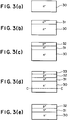
- FIGS.3(a) to 3(e) are a flow chart illustrating an example of a third embodiment of the present invention.
- a phosphorous doped n ⁇ - silicon substrate 30 which was grown by a FZ method and had a surface orientation of( 100 ), a resistivity of 80 ⁇ cm, a diameter of 125 mm, and an initial thickness of 550 ⁇ m(FIG.3(a)), was used.
- a phosphorous doped n+- buffer layer 31 of a resistivity of 0.1 ⁇ cm and of 10 ⁇ m thick was epitaxially grown (FIG.3(b)); then, a boron doped p+- layer 32 of a resistivity of 0.015 ⁇ cm and of 200 ⁇ m thick ( FIG.3(c) ) and an undoped silicon layer 33 of a resistivity larger than 0.15 ⁇ cm and of 100 ⁇ m thick respectively were epitaxially grown in the sequence of the written order (FIG.3(d)); and in the last step, the backside surface of the n ⁇ - silicon substrate 30 was ground and polished to expose a ground and polished surface corresponding to a dash line C - C, while the undoped silicon layer 33 was also processed to be removed, so that a substrate for IGBT of the total thickness of about 500 ⁇ m thick, where the thickness of the n ⁇ - silicon substrate 30 was about 300 ⁇ m, was obtained (FIG.3(e)).
- the bow and slippage density of the substrate for IGBT produced by the aforementioned method was measured.
- This substrate had bow on the order of 25 ⁇ m, though the bow being a concave on the p+ - layer side, and the slip dislocation density in the n ⁇ -silicon substrate was 1 x 10³ dislocations/cm.
- a substrate for IGBT was produced under the same conditions as in EXAMPLE 1, except that a silicon nitride film was not formed on the backside surface of a substrate.
- n+- buffer layers 12, 21 and 31 were grown by an epitaxial growth method, but even when n+- buffer layers were formed by a diffusion method or ion implantation method instead of an epitaxial growth method, results similar to the aforementioned were obtained.
- the impurity concentration of each layer is precisely controlled and thereby the resistivity is also stabilised, since occurrence of autodoping can be prevented.
- a substrate for IGBT production of a semiconductor substrate more suitable for IGBT becomes a real possibility, since fabrication of an IGBT having a high withstand voltage becomes easy due to the use of the silicon substrate of a high resistivity and besides the density of slip dislocations in the substrate can be reduced.
Landscapes
- Recrystallisation Techniques (AREA)
- Mechanical Treatment Of Semiconductor (AREA)
- Insulated Gate Type Field-Effect Transistor (AREA)
Applications Claiming Priority (3)
| Application Number | Priority Date | Filing Date | Title |
|---|---|---|---|
| JP23047694 | 1994-08-31 | ||
| JP06230476A JP3113156B2 (ja) | 1994-08-31 | 1994-08-31 | 半導体基板の製造方法 |
| JP230476/94 | 1994-08-31 |
Publications (3)
| Publication Number | Publication Date |
|---|---|
| EP0702401A2 true EP0702401A2 (de) | 1996-03-20 |
| EP0702401A3 EP0702401A3 (de) | 1996-07-10 |
| EP0702401B1 EP0702401B1 (de) | 1999-08-11 |
Family
ID=16908414
Family Applications (1)
| Application Number | Title | Priority Date | Filing Date |
|---|---|---|---|
| EP95306038A Expired - Lifetime EP0702401B1 (de) | 1994-08-31 | 1995-08-30 | Verfahren zur Herstellung eines für IGBT geeigneten Halbleiterplättchens |
Country Status (4)
| Country | Link |
|---|---|
| US (1) | US5696034A (de) |
| EP (1) | EP0702401B1 (de) |
| JP (1) | JP3113156B2 (de) |
| DE (1) | DE69511343T2 (de) |
Cited By (5)
| Publication number | Priority date | Publication date | Assignee | Title |
|---|---|---|---|---|
| EP1017093A1 (de) * | 1998-12-29 | 2000-07-05 | ABB Semiconductors AG | Leistungshalbleiterelement und Verfahren zur Herstellung |
| WO2002003469A1 (de) * | 2000-07-04 | 2002-01-10 | Abb Schweiz Ag | Halbleiter leistungsbauelement und verfahren zu seiner herstellung |
| EP1297567A4 (de) * | 2000-05-05 | 2008-03-19 | Int Rectifier Corp | Wasserstoffimplantation f r eine pufferzone eines punch-through-nicht-epi-igbt |
| CN102054690A (zh) * | 2010-11-22 | 2011-05-11 | 复旦大学 | 一种用于制造大功率器件的半导体衬底的制造方法 |
| CN107845570A (zh) * | 2017-11-09 | 2018-03-27 | 四川广瑞半导体有限公司 | 绝缘栅双极型晶体管的硅外延片生产工艺 |
Families Citing this family (6)
| Publication number | Priority date | Publication date | Assignee | Title |
|---|---|---|---|---|
| WO2002048811A1 (fr) | 2000-12-14 | 2002-06-20 | Mitsubishi Denki Kabushiki Kaisha | Organe de commande numerique et procede de commande de l'arbre de cet organe |
| US8685427B2 (en) * | 2002-07-31 | 2014-04-01 | Boston Scientific Scimed, Inc. | Controlled drug delivery |
| US8920826B2 (en) | 2002-07-31 | 2014-12-30 | Boston Scientific Scimed, Inc. | Medical imaging reference devices |
| WO2014041736A1 (ja) * | 2012-09-13 | 2014-03-20 | パナソニック株式会社 | 窒化物半導体構造物 |
| CN104112663A (zh) * | 2013-04-18 | 2014-10-22 | 比亚迪股份有限公司 | 一种半导体结构及其形成方法 |
| CN107845695B (zh) * | 2017-12-08 | 2024-01-16 | 苏州矩阵光电有限公司 | 一种晶体外延结构及生长方法 |
Family Cites Families (9)
| Publication number | Priority date | Publication date | Assignee | Title |
|---|---|---|---|---|
| DE1286511B (de) * | 1964-12-19 | 1969-01-09 | Telefunken Patent | Verfahren zum Herstellen eines Halbleiterkoerpers mit einem niederohmigen Substrat |
| JPS5392673A (en) * | 1977-01-24 | 1978-08-14 | Mitsubishi Electric Corp | Manufacture of semiconductor |
| JPS5394778A (en) * | 1977-01-31 | 1978-08-19 | Toshiba Corp | Manufacture of semiconductor device |
| JPS60157254A (ja) * | 1984-01-26 | 1985-08-17 | Meidensha Electric Mfg Co Ltd | ゲ−トタ−ンオフサイリスタ構造及びその製造方法 |
| JPS60171722A (ja) * | 1984-02-17 | 1985-09-05 | Toshiba Corp | 半導体素子の製造方法 |
| JPH0724312B2 (ja) * | 1988-06-10 | 1995-03-15 | 三菱電機株式会社 | 半導体装置の製造方法 |
| JP2645478B2 (ja) * | 1988-10-07 | 1997-08-25 | 富士通株式会社 | 半導体装置の製造方法 |
| JPH04286163A (ja) * | 1991-03-14 | 1992-10-12 | Shin Etsu Handotai Co Ltd | 半導体基板の製造方法 |
| JP2911694B2 (ja) * | 1992-10-29 | 1999-06-23 | 信越半導体株式会社 | 半導体基板及びその製造方法 |
-
1994
- 1994-08-31 JP JP06230476A patent/JP3113156B2/ja not_active Expired - Fee Related
-
1995
- 1995-08-28 US US08/520,189 patent/US5696034A/en not_active Expired - Fee Related
- 1995-08-30 EP EP95306038A patent/EP0702401B1/de not_active Expired - Lifetime
- 1995-08-30 DE DE69511343T patent/DE69511343T2/de not_active Expired - Fee Related
Non-Patent Citations (1)
| Title |
|---|
| None |
Cited By (9)
| Publication number | Priority date | Publication date | Assignee | Title |
|---|---|---|---|---|
| EP1017093A1 (de) * | 1998-12-29 | 2000-07-05 | ABB Semiconductors AG | Leistungshalbleiterelement und Verfahren zur Herstellung |
| EP1297567A4 (de) * | 2000-05-05 | 2008-03-19 | Int Rectifier Corp | Wasserstoffimplantation f r eine pufferzone eines punch-through-nicht-epi-igbt |
| WO2002003469A1 (de) * | 2000-07-04 | 2002-01-10 | Abb Schweiz Ag | Halbleiter leistungsbauelement und verfahren zu seiner herstellung |
| US6825110B2 (en) | 2000-07-04 | 2004-11-30 | Abb Schweiz Ag | Method for fabricating semiconductor component with an optimized thickness |
| RU2274929C2 (ru) * | 2000-07-04 | 2006-04-20 | Абб Швайц Аг | Полупроводниковый элемент и способ его изготовления |
| CN102054690A (zh) * | 2010-11-22 | 2011-05-11 | 复旦大学 | 一种用于制造大功率器件的半导体衬底的制造方法 |
| CN102054690B (zh) * | 2010-11-22 | 2012-10-17 | 复旦大学 | 一种用于制造大功率器件的半导体衬底的制造方法 |
| CN107845570A (zh) * | 2017-11-09 | 2018-03-27 | 四川广瑞半导体有限公司 | 绝缘栅双极型晶体管的硅外延片生产工艺 |
| CN107845570B (zh) * | 2017-11-09 | 2019-02-12 | 四川广瑞半导体有限公司 | 绝缘栅双极型晶体管的硅外延片生产工艺 |
Also Published As
| Publication number | Publication date |
|---|---|
| JPH0878679A (ja) | 1996-03-22 |
| JP3113156B2 (ja) | 2000-11-27 |
| DE69511343T2 (de) | 2000-03-30 |
| EP0702401B1 (de) | 1999-08-11 |
| EP0702401A3 (de) | 1996-07-10 |
| DE69511343D1 (de) | 1999-09-16 |
| US5696034A (en) | 1997-12-09 |
Similar Documents
| Publication | Publication Date | Title |
|---|---|---|
| US5311055A (en) | Trenched bipolar transistor structures | |
| US5562770A (en) | Semiconductor manufacturing process for low dislocation defects | |
| US6083812A (en) | Heteroepitaxy by large surface steps | |
| US4579621A (en) | Selective epitaxial growth method | |
| US20070249142A1 (en) | Semiconductor devices and method of manufacturing them | |
| JPH04230037A (ja) | インサイチュ・ドープされたn型シリコン層の付着方法およびNPNトランジスタ | |
| US5696034A (en) | Method for producing semiconductor substrate | |
| JP3024584B2 (ja) | 半導体装置の製造方法 | |
| EP0501119B1 (de) | Verfahren zur Herstellung eines Halbleitersubstrats | |
| US5998283A (en) | Silicon wafer having plasma CVD gettering layer with components/composition changing in depth-wise direction and method of manufacturing the silicon wafer | |
| EP0449589A1 (de) | Verfahren zur Herstellung einer SOI-Struktur | |
| US7276416B2 (en) | Method of forming a vertical transistor | |
| EP0633606A1 (de) | Verfahren zur Herstellung einer Leistungsdiode | |
| JP2911694B2 (ja) | 半導体基板及びその製造方法 | |
| US8102052B2 (en) | Process for the simultaneous deposition of crystalline and amorphous layers with doping | |
| JPH0563439B2 (de) | ||
| EP0632486A2 (de) | Epitaktischer Halbleitermaterial und Herstellungsverfahren | |
| US20020053316A1 (en) | Method of deposition of a single-crystal silicon region | |
| US4686762A (en) | Fabricating semiconductor device with polysilicon protection layer during processing | |
| EP0822274A2 (de) | Verfahren zur Herstellung eines epitaktischen Wafers | |
| JP4329211B2 (ja) | 炭化珪素単結晶を用いた炭化珪素半導体装置およびその製造方法 | |
| JP4826373B2 (ja) | 単結晶ウェハの製造方法 | |
| JPH0196923A (ja) | エピタキシャル成長方法 | |
| JPH0714840B2 (ja) | エピタキシャル膜成長方法 | |
| US3834958A (en) | Method for isolation of circuit regions in monolithic integrated circuit structure |
Legal Events
| Date | Code | Title | Description |
|---|---|---|---|
| PUAI | Public reference made under article 153(3) epc to a published international application that has entered the european phase |
Free format text: ORIGINAL CODE: 0009012 |
|
| AK | Designated contracting states |
Kind code of ref document: A2 Designated state(s): DE FR GB |
|
| PUAL | Search report despatched |
Free format text: ORIGINAL CODE: 0009013 |
|
| AK | Designated contracting states |
Kind code of ref document: A3 Designated state(s): DE FR GB |
|
| 17P | Request for examination filed |
Effective date: 19960816 |
|
| 17Q | First examination report despatched |
Effective date: 19970612 |
|
| GRAG | Despatch of communication of intention to grant |
Free format text: ORIGINAL CODE: EPIDOS AGRA |
|
| GRAG | Despatch of communication of intention to grant |
Free format text: ORIGINAL CODE: EPIDOS AGRA |
|
| GRAG | Despatch of communication of intention to grant |
Free format text: ORIGINAL CODE: EPIDOS AGRA |
|
| GRAH | Despatch of communication of intention to grant a patent |
Free format text: ORIGINAL CODE: EPIDOS IGRA |
|
| GRAH | Despatch of communication of intention to grant a patent |
Free format text: ORIGINAL CODE: EPIDOS IGRA |
|
| GRAA | (expected) grant |
Free format text: ORIGINAL CODE: 0009210 |
|
| PGFP | Annual fee paid to national office [announced via postgrant information from national office to epo] |
Ref country code: FR Payment date: 19990810 Year of fee payment: 5 |
|
| AK | Designated contracting states |
Kind code of ref document: B1 Designated state(s): DE FR GB |
|
| PGFP | Annual fee paid to national office [announced via postgrant information from national office to epo] |
Ref country code: GB Payment date: 19990825 Year of fee payment: 5 |
|
| PGFP | Annual fee paid to national office [announced via postgrant information from national office to epo] |
Ref country code: DE Payment date: 19990827 Year of fee payment: 5 |
|
| REF | Corresponds to: |
Ref document number: 69511343 Country of ref document: DE Date of ref document: 19990916 |
|
| ET | Fr: translation filed | ||
| PLBE | No opposition filed within time limit |
Free format text: ORIGINAL CODE: 0009261 |
|
| STAA | Information on the status of an ep patent application or granted ep patent |
Free format text: STATUS: NO OPPOSITION FILED WITHIN TIME LIMIT |
|
| 26N | No opposition filed | ||
| PG25 | Lapsed in a contracting state [announced via postgrant information from national office to epo] |
Ref country code: GB Free format text: LAPSE BECAUSE OF NON-PAYMENT OF DUE FEES Effective date: 20000830 |
|
| GBPC | Gb: european patent ceased through non-payment of renewal fee |
Effective date: 20000830 |
|
| PG25 | Lapsed in a contracting state [announced via postgrant information from national office to epo] |
Ref country code: FR Free format text: LAPSE BECAUSE OF NON-PAYMENT OF DUE FEES Effective date: 20010430 |
|
| PG25 | Lapsed in a contracting state [announced via postgrant information from national office to epo] |
Ref country code: DE Free format text: LAPSE BECAUSE OF NON-PAYMENT OF DUE FEES Effective date: 20010501 |
|
| REG | Reference to a national code |
Ref country code: FR Ref legal event code: ST |